
256K x 18, 128K x 32, 128K x 36 4Mb Sync Burst SRAMs 180 MHz–100 MHz
3.3 V V DD 3.3 V and 2.5 V I/O
TQFP, BGA Commercial Temp Industrial Temp
Features
? FT pin for user-configurable flow through or pipelined operation
? Single Cycle Deselect (SCD) operation
? 3.3 V +10%/–5% core power supply
? 2.5 V or 3.3 V I/O supply
? LBO pin for Linear or Interleaved Burst mode
? Internal input resistors on mode pins allow floating mode pins ? Default to Interleaved Pipelined mode
? Byte Write (BW) and/or Global Write (GW) operation
? Common data inputs and data outputs
? Clock control, registered, address, data, and control
? Internal self-timed write cycle
? Automatic power-down for portable applications
? JEDEC standard 100-lead TQFP or 119-Bump BGA package
Functional Description
Applications
The GS84018/32/36A is a 4,718,592-bit (4,194,304-bit for
x32 version) high performance synchronous SRAM with a 2-bit burst address counter. Although of a type originally developed for Level 2 Cache applications supporting high performance CPUs, the device now finds application in synchronous SRAM applications ranging from DSP main store to networking chip set support. The GS84018/32/36A is available in a JEDEC standard 100-lead TQFP or 119-Bump BGA package.
Controls
Addresses, data I/Os, chip enables (E1, E2, E3), address burst control inputs (ADSP, ADSC, ADV), and write control inputs (Bx, BW, GW) are synchronous and are controlled by a positive-edge-triggered clock input (CK). Output enable (G) and power down control (ZZ) are asynchronous inputs. Burst cycles can be initiated with either ADSP or ADSC inputs. In Burst mode, subsequent burst addresses are generated internally and are controlled by ADV. The burst address counter may be configured to count in either linear or interleave order with the Linear Burst Order (LBO) input. The burst function need not be used. New addresses can be loaded on every cycle with no degradation of chip performance. Flow Through/Pipeline Reads
The function of the Data Output register can be controlled by the user via the FT mode pin/bump (pin 14 in the TQFP and bump 5R in the BGA). Holding the FT mode pin/bump low places the RAM in Flow Through mode, causing output data to bypass the Data Output Register. Holding FT high places the RAM in Pipelined mode, activating the rising-edge-triggered Data Output Register.
SCD Pipelined Reads
The GS84018/32/36A is an SCD (Single Cycle Deselect) pipelined synchronous SRAM. DCD (Dual Cycle Deselect) versions are also available. SCD SRAMs pipeline deselect commands one stage less than read commands. SCD RAMs begin turning off their outputs immediately after the deselect command has been captured in the input registers.
Byte Write and Global Write
Byte write operation is performed by using byte write enable (BW) input combined with one or more individual byte write signals (Bx). In addition, Global Write (GW) is available for writing all bytes at one time, regardless of the Byte Write control inputs.
Sleep Mode
Low power (Sleep mode) is attained through the assertion (High) of the ZZ signal, or by stopping the clock (CK). Memory data is retained during Sleep mode.
Core and Interface Voltages
The GS84018/32/36A operates on a 3.3 V power supply and all inputs/outputs are 3.3 V- and 2.5 V-compatible. Separate output power (V DDQ) pins are used to de-couple output noise from the internal circuit.
–180–166–150–100
Pipeline 3-1-1-1tCycle
t KQ
I DD
5.5 ns
3.0 ns
185 mA
6.0 ns
3.5 ns
170 mA
6.6 ns
3.8 ns
155 mA
10 ns
4.5 ns
105 mA
Flow Through 2-1-1-1
t KQ
tCycle
I DD
8 ns
9.1 ns
115 mA
8.5 ns
10 ns
105 mA
10 ns
12 ns
100 mA
12 ns
15 ns
80 mA
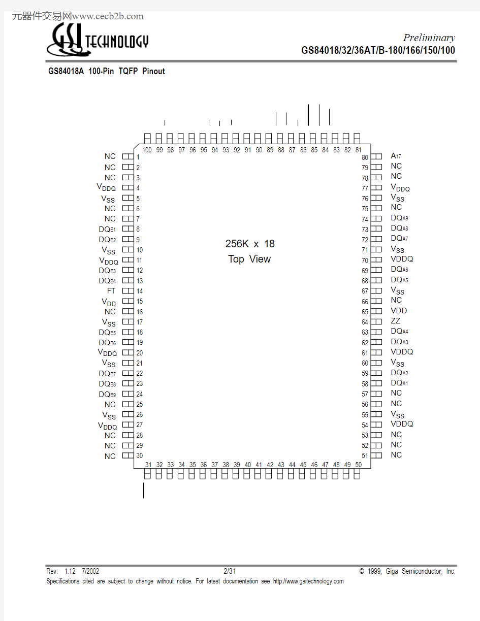
GS84018A 100-Pin TQFP Pinout
807978777675747372
71
7069686766656463626160595857565554535251123456789101112131415161718192021222324252627282930V DDQ V SS DQ B1DQ B2V SS V DDQ DQ B3DQ B4
V DD NC V SS DQ B5DQ B6V DDQ V SS DQ B7DQ B8DQ B9V SS V DDQ V DDQ V SS DQ A8DQ A7V SS VDDQ DQ A6DQ A5V SS NC VDD ZZ DQ A4DQ A3VDDQ V SS DQ A2DQ A1V SS VDDQ L B O A 5
A 4
A 3
A 2
A 1
A 0
N C N C V S S
V D D
N C N C A 10
A 11
A 12
A 13
A 14
A 16
A 6
A 7
E 1
E 2 N C N C B B
B A
E 3
C K G W B W V
D D
V S S
G A D S C A D S P A D V A 8
A 9
A 15
256K x 18Top View DQ A9A 17NC NC NC NC NC NC NC NC
NC NC NC NC NC NC NC
NC NC 100999897969594939291908988878685848382813132333435363738394041424344454647484950
FT
GS84032A 100-Pin TQFP Pinout
807978777675747372
71
7069686766656463626160595857565554535251123456789101112131415161718192021222324252627282930V DDQ V SS DQ C4DQ C3V SS V DDQ DQ C2DQ C1V DD NC V SS DQ D1DQ D2V DDQ V SS DQ D3DQ D4DQ D5V SS V DDQ V DDQ V SS DQ B4DQ B3V SS V DDQ DQ B2DQ B1V SS NC V DD ZZ DQ A1DQ A2V DDQ V SS DQ A3DQ A4V SS V DDQ L B O A 5
A 4
A 3
A 2
A 1
A 0
N C N C V S S
V D D
N C N C A 10
A 11
A 12
A 13
A 14
A 16
A 6
A 7
E 1
E 2 B D
B C
B B
B A
E 3
C K G W B W V
D D
V S S
G A D S C A D S P A D V A 8
A 9
A 15
128K x 32Top View DQ B5NC DQ B7DQ B8DQ B6DQ A6DQ A5DQ A8DQ A7NC
DQ C7DQ C8DQ C6DQ D6DQ D8DQ D7NC
DQ C5NC 100999897969594939291908988878685848382813132333435363738394041424344454647484950
FT
GS84036A 100-Pin TQFP Pinout
807978777675747372
71
7069686766656463626160595857565554535251123456789101112131415161718192021222324252627282930V DDQ V SS DQ C4DQ C3V SS V DDQ DQ C2DQ C1
V DD NC V SS DQ D1DQ D2V DDQ V SS DQ D3DQ D4DQ D5V SS V DDQ V DDQ V SS DQ B4DQ B3V SS V DDQ DQ B2DQ B1V SS NC V DD ZZ DQ A1DQ A2V DDQ V SS DQ A3DQ A4V SS V DDQ L B O A 5
A 4
A 3
A 2
A 1
A 0
N C N C V S S
V D D
N C N C A 10
A 11
A 12
A 13
A 14
A 16
A 6
A 7
E 1
E 2 B D
B C
B B
B A
E 3
C K G W B W V
D D
V S S
G A D S C A D S P A D V A 8
A 9
A 15
128K x 36Top View DQ B5DQ B9DQ B7DQ B8DQ B6DQ A6DQ A5DQ A8DQ A7DQ A9
DQ C7DQ C8DQ C6DQ D6DQ D8DQ D7DQ D9
DQ C5DQ C9100999897969594939291908988878685848382813132333435363738394041424344454647484950
FT
TQFP Pin Description
Pin Location Symbol Type Description
37, 36A0, A1I Address field LSBs and Address Counter preset Inputs 35, 34, 33, 32, 100, 99, 82, 81,44, 45, 46,
47, 48, 49, 50
A2–A16I Address Inputs
80A17I Address Inputs (x18 versions)
52, 53, 56, 57, 58, 59, 62, 63 68, 69, 72, 73, 74, 75, 78, 79 2, 3, 6, 7, 8, 9, 12, 13 18, 19, 22, 23, 24, 25, 28, 29DQ A1–DQ A8
DQ B1–DQ B8
DQ C1–DQ C8
DQ D1–DQ D8
I/O Data Input and Output pins. (x32, x36 Version)
51, 80, 1, 30DQ A9, DQ B9,
DQ C9, DQ D9
I/O Data Input and Output pins (x36 Version)
51, 80, 1, 30NC No Connect (x32 Version)
58, 59, 62, 63, 68, 69, 72, 73, 74 8, 9, 12, 13, 18, 19, 22, 23, 24DQ A1–DQ A9
DQ B1–DQ B9
I/O Data Input and Output pins (x18 Version)
51, 52, 53, 56, 57
75, 78, 79
1, 2, 3, 6, 7
25, 28, 29, 30
NC-No Connect (x18 Version)
87BW I Byte Write—Writes all enabled bytes; active low 93, 94B A, B B I Byte Write Enable for DQ A, DQ B Data I/’s; active low
95, 96B C, B D I Byte Write Enable for DQ C, DQ D Data I/Os; active low
(x32, x36 Version)
95, 96NC-No Connect (x18 Version)
89CK I Clock Input Signal; active high
88GW I Global Write Enable—Writes all bytes; active low
98, 92E1, E3I Chip Enable; active low
97E2I Chip Enable; active high
86G I Output Enable; active low
83ADV I Burst address counter advance enable; active low
84, 85ADSP, ADSC I Address Strobe (Processor, Cache Controller); active low
64ZZ I Sleep Mode control; active high
14FT I Flow Through or Pipeline mode; active low
31LBO I Linear Burst Order mode; active low 15, 41, 65, 91V DD I Core power supply
5,10,17, 21, 26, 40, 55, 60, 67, 71, 76, 90V SS I I/O and Core Ground 4, 11, 20, 27, 54, 61, 70, 77V DDQ I Output driver power supply
16, 38, 39, 42, 43, 66NC-No Connect
119-Bump BGA—Top View
1234567
A V DDQ A6A7ADSP A8A9V DDQ
B N
C E2A4ADSC A15E3NC
C NC A5A3V D
D A14A16NC
D DQ B1NC V SS NC V SS DQ A9NC
E NC DQ B2V SS E1V SS NC DQ A8
F V DDQ NC V SS
G V SS DQ A7V DDQ
G NC D Q B3B B ADV NC NC DQ A6
H DQ B4N C V SS GW V SS DQ A5NC J V DDQ V DD NC V DD NC V DD V DDQ K NC DQ B5V SS CK V SS NC DQ A4 L DQ B6NC NC NC B A DQ A3NC M V DDQ DQ B7V SS BW V SS NC V DDQ N DQ B8NC V SS A1V SS DQ A2NC P NC DQ B9V SS A0V SS NC DQ A1 R NC A2LBO V DD FT A13NC T NC A10A11NC A12 A17ZZ U V DDQ NC NC NC NC NC V DDQ
119-Bump BGA—Top View
1234567
A V DDQ A6A7ADSP A8A9V DDQ
B N
C E2A4ADSC A15E3NC
C NC A5A3V D
D A14A16NC
D DQ C4NC V SS NC V SS NC DQ B4
E DQ C3DQ C8V SS E1V SS DQ B8DQ B3
F V DDQ DQ C7V SS
G V SS DQ B7V DDQ
G DQ C2D Q C6B C ADV B B DQ B6DQ B2
H DQ C1DQ C5V SS GW V SS DQ B5DQ B1 J V DDQ V DD NC V DD NC V DD V DDQ K DQ D1DQ D5V SS CK V SS DQ A5DQ A1 L DQ D2DQ D6B D NC B A DQ A6DQ A2 M V DDQ DQ D78V SS BW V SS DQ A7V DDQ N DQ D3DQ D8V SS A1V SS DQ A8DQ A3 P DQ D4NC V SS A0V SS NC DQ A4 R NC A2LBO V DD FT A13NC T NC NC A10A11A12 NC ZZ U V DDQ NC NC NC NC NC V DDQ
119-Bump BGA—Top View
1234567
A V DDQ A6A7ADSP A8A9V DDQ
B N
C E2A4ADSC A15E3NC
C NC A5A3V D
D A14A16NC
D DQ C4DQ C9V SS NC V SS DQ B9DQ B4
E DQ C3DQ C8V SS E1V SS DQ B8DQ B3
F V DDQ DQ C7V SS
G V SS DQ B7V DDQ
G DQ C2D Q C6B C ADV B B DQ B6DQ B2
H DQ C1DQ C5V SS GW V SS DQ B5DQ B1 J V DDQ V DD NC V DD NC V DD V DDQ K DQ D1DQ D5V SS CK V SS DQ A5DQ A1 L DQ D2DQ D6B D NC B A DQ A6DQ A2 M V DDQ DQ D78V SS BW V SS DQ A7V DDQ N DQ D3DQ D8V SS A1V SS DQ A8DQ A3 P DQ D4DQ D9V SS A0V SS DQ A9DQ A4 R NC A2LBO V DD FT A13NC T NC NC A10A11A12 NC ZZ U V DDQ NC NC NC NC NC V DDQ
BGA Pin Description
Pin Location Symbol Type Description
N4, P4A0, A1I Address field LSBs and Address Counter Preset Inputs A2, A3, A5, A6, B3, B5, C2, C3, C5,
C6, R2, R6, T3, T5
An I Address Inputs
T4An Address Input (x32/36 Versions)
T2, T6NC-No Connect (x32/36 Versions)
T2, T6An I Address Input (x18 Version)
K7, K6, L7, L6, M6, N7, N6, P7 H7, H6, G7, G6, F6, E7, E6, D7 H1, H2, G1, G2, F2, E1, E2, D1 K1, K2, L1, L2, M2, N1, N2, P1DQ A1-DQ A8
DQ B1-DQ B8
DQ C1-DQ C8
DQ D1-DQ D8
I/O Data Input and Output pins (x32/36 Versions)
P6, D6, D2, P2DQ A9, DQ B9,
DQ C9, DQ D9
I/O Data Input and Output pins (x36 Version)
P6, D6, D2, P2NC-No Connect (x32 Version)
L5, G5, G3, L3B A, B B, B C, B D I Byte Write Enable for DQ A, DQ B, DQ C, DQ D I/O’s; active low ( x36 Version)
P7, N6, L6, K7, H6, G7, F6, E7, D6 D1, E2, G2, H1, K2, L1, M2, N1, P2DQ A1-DQ A9
DQ B1-DQ B9
I/O Data Input and Output pins (x18 Version)
L5, G3B A, B B I Byte Write Enable for DQ A, DQ B I/O’s; active low ( x18 Version) B1, C1, R1, T1, U2, J3, U3, D4, L4,
U4, J5, U5, U6, B7, C7, R7
NC-No Connect
P6, N7, M6, L7, K6, H7, G6, E6, D7,
D2, B1, E1, F2, G1, H2, K1, L2, N2,
P1, G5, L3, T4
NC-No Connect (x18 Version)
K4CK I Clock Input Signal; active high
M4BW I Byte Write—Writes all enabled bytes; active low
H4GW I Global Write Enable—Writes all bytes; active low
E4, B6E1, E3I Chip Enable; active low
B2E2I Chip Enable; active high
F4G I Output Enable; active low
G4ADV I Burst address counter advance enable; active low
A4, B4ADSP, ADSC I Address Strobe (Processor, Cache Controller); active low
T7ZZ I Sleep Mode control; active high
R5FT I Flow Through or Pipeline mode; active low
R3LBO I Linear Burst Order mode; active low J2, C4, J4, R4, J6V DD I Core power supply
D3, E3, F3, H3, K3, M3, N3, P3, D5,
E5, F5, H5, K5, M5, N5, P5
V SS I I/O and Core Ground
A1, F1, J1, M1, U1, A7, F7, J7, M7,
U7
V DDQ I Output driver power supply
GS84018/32/36A Block Diagram
A1
A0
A0A1
D0
D1Q1Q0
Counter Load
D Q
D
Q
Register
Register
D
Q
Register
D
Q
Register
D
Q
Register
D Q
Register
D Q
Register
D
Q
Register
D
Q
R e g i s t e r
D
Q
Register
A0–An LBO ADV CK ADSC ADSP GW BW B A
B B
B C
B D
E 1G
ZZ
Power Down Control
Memory Array
36
36
4
A
Q
D
E 3E 2
DQx0–DQx9
Note: Only x36 version shown for simplicity.
1
FT
Note:
There are pull-up devices on LBO and FT pins and a pull down device on the ZZ pin, so those input pins can be unconnected and the chip will operate in the default states as specified in the above tables.
Burst Counter Sequences
Byte Write Truth Table
Notes:
1.All byte outputs are active in read cycles regardless of the state of Byte Write Enable inputs.
2.Byte Write Enable inputs B A , B B , B C and/or B D may be used in any combination with BW to write single or multiple bytes.
3.All byte I/Os remain High-Z during all write operations regardless of the state of Byte Write Enable inputs.
4.Bytes “C ” and “D ” are only available on the x32 and x36 versions.Mode Pin Functions Mode Name
Pin
Name
State
Function
Burst Order Control LBO L Linear Burst H or NC Interleaved Burst Output Register Control FT L Flow Through H or NC Pipeline Power Down Control
ZZ
L or NC Active H
Standby, I DD = I SB
Function
GW
BW
B A
B B
B C
B D
Notes
Read H H X X X X 1Read H L H H H H 1Write byte A H L L H H H 2,
3Write byte B H L H L H H 2, 3Write byte C H L H H L H 2, 3, 4Write byte D H L H H H L 2, 3, 4Write all
bytes H L L L L L 2, 3, 4
Write all bytes
L
X
X
X
X
X
Linear Burst Sequence
Note: The burst counter wraps to initial state on the 5th clock.
I nterleaved Burst Sequence
Note: The burst counter wraps to initial state on the 5th clock.
A[1:0]A[1:0]A[1:0]A[1:0]
1st address 000110112nd address 011011003rd address 101100014th address
11
00
01
10
A[1:0]A[1:0]A[1:0]A[1:0]
1st address 000110112nd address 010011103rd address 101100014th address
11
10
01
00
Synchronous Truth Table
Operation Address
Used
State
Diagram
Key5
E1E2ADSP ADSC ADV W3DQ4
Deselect Cycle, Power Down None X H X X L X X High-Z Deselect Cycle, Power Down None X L F L X X X High-Z Deselect Cycle, Power Down None X L F H L X X High-Z Read Cycle, Begin Burst External R L T L X X X Q Read Cycle, Begin Burst External R L T H L X F Q Write Cycle, Begin Burst External W L T H L X T D Read Cycle, Continue Burst Next CR X X H H L F Q Read Cycle, Continue Burst Next CR H X X H L F Q Write Cycle, Continue Burst Next CW X X H H L T D Write Cycle, Continue Burst Next CW H X X H L T D Read Cycle, Suspend Burst Current X X H H H F Q Read Cycle, Suspend Burst Current H X X H H F Q Write Cycle, Suspend Burst Current X X H H H T D Write Cycle, Suspend Burst Current H X X H H T D Notes:
1.X = Don’t Care, H = High, L = Low.
2. E = T (True) if E2 = 1 and E3 = 0; E = F (False) if E2 = 0 or E3 = 1.
3.W = T (True) and F (False) is defined in the Byte Write Truth Table preceding.
4.G is an asynchronous input. G can be driven high at any time to disable active output drivers. G low can only enable active drivers (shown
as “Q” in the Truth Table above).
5.All input combinations shown above are tested and supported. Input combinations shown in gray boxes need not be used to accomplish
basic synchronous or synchronous burst operations and may be avoided for simplicity.
6.Tying ADSP high and ADSC low allows simple non-burst synchronous operations. See BOLD items above.
7.Tying ADSP high and ADV low while using ADSC to load new addresses allows simple burst operations. See ITALIC items above.
First Write
First Read
Burst Write
Burst Read
Deselect
R W
CR
CW
X X
W
R
R
W
R
X
X
X S i m p l e S y n c h r o n o u s O p e r a t i o n
S i m p l e B u r s t S y n c h r o n o u s O p e r a t i o n
CR R
CW
CR
CR
Simplified State Diagram
Notes:
1.The diagram shows only supported (tested) synchronous state transitions. The diagram presumes G is tied Low.
2.The upper portion of the diagram assumes active use of only the Enable (E 1, E 2, E 3) and Write (B A , B B , B C , B D , BW and GW) control inputs
and that ADSP is tied high and ADSC is tied low.
3.The upper and lower portions of the diagram together assume active use of only the Enable, Write and ADSC control inputs and assumes
ADSP is tied high and ADV is tied low.
First Write
First Read
Burst Write
Burst Read
Deselect
R W
CR
CW
X
X
W
R
R
W
R
X
X
X CR
R CW CR
CR
W CW
W CW
Simplified State Diagram with G
Notes:
1.The diagram shows supported (tested) synchronous state transitions plus supported transitions that depend upon the use of G.
https://www.doczj.com/doc/fa17600244.html,e of “Dummy Reads” (Read Cycles with G High) may be used to make the transition from Read cycles to Write cycles without passing
through a Deselect cycle. Dummy Read cycles increment the address counter just like normal Read cycles.
3.Transitions shown in grey tone assume G has been pulsed high long enough to turn the RAM’s drivers off and for incoming data to meet
Data Input Set Up Time.
Absolute Maximum Ratings
(All voltages reference to V SS)
Symbol Description Value Unit
V DD Voltage on V DD Pins–0.5 to 4.6V
V DDQ Voltage in V DDQ Pins–0.5 to V DD V
V CK Voltage on Clock Input Pin–0.5 to 6V
V I/O Voltage on I/O Pins–0.5 to V DDQ +0.5 (≤ 4.6 V max.)V
V IN Voltage on Other Input Pins–0.5 to V DD +0.5 (≤ 4.6 V max.)V
I IN Input Current on Any Pin+/–20mA
I OUT Output Current on Any I/O Pin+/–20mA
P D Package Power Dissipation 1.5W
T STG Storage Temperature–55 to 125o C
T BIAS Temperature Under Bias–55 to 125o C
Note:
Permanent damage to the device may occur if the Absolute Maximum Ratings are exceeded. Operation should be restricted to Rec-ommended Operating Conditions. Exposure to conditions exceeding the Absolute Maximum Ratings, for an extended period of time, may affect reliability of this component.
Recommended Operating Conditions
Parameter Symbol Min.Typ.Max.Unit Notes Supply Voltage V DD 3.135 3.3 3.6V
I/O Supply Voltage V DDQ 2.375 2.5V DD V1
Input High Voltage V IH 1.7—V DD +0.3V2
Input Low Voltage V IL–0.3—0.8V2 Ambient Temperature (Commercial Range Versions)T A02570°C3 Ambient Temperature (Industrial Range Versions)T A–402585°C3 Note:
1.Unless otherwise noted, all performance specifications quoted are evaluated for worst case at both
2.75 V ≤ V DDQ ≤ 2.375 V
(i.e., 2.5 V I/O) and 3.6 V ≤ V DDQ≤ 3.135 V (i.e., 3.3 V I/O) and quoted at whichever condition is worst case.
2.This device features input buffers compatible with both
3.3 V and 2.5 V I/O drivers.
3.Most speed grades and configurations of this device are offered in both Commercial and Industrial Temperature ranges. The part number of
Industrial Temperature Range versions end the character “I”. Unless otherwise noted, all performance specifications quoted are evaluated for worst case in the temperature range marked on the device.
4.Input Under/overshoot voltage must be –2 V > Vi < V DD+2 V with a pulse width not to exceed 20% tKC.
Note: This parameter is sample tested.
Notes:
1.Junction temperature is a function of SRAM power dissipation, package thermal resistance, mounting board temperature, ambient. Temper-ature air flow, board density, and PCB thermal resistance.
2.SCMI G-38-87.
3.Average thermal resistance between die and top surface, MIL SPEC-883, Method 1012.1.
4. For x18 configuration, consult factory.
Capacitance
(T A = 25o C, f = 1 MH Z , V DD = 3.3 V)
Parameter
Symbol
Test conditions
Typ.
Max.
Unit
Control Input Capacitance C I V DD = 3.3 V 34pF Input Capacitance
C IN V IN = 0 V 45pF Output Capacitance
C OUT
V OUT = 0 V
6
7
pF
Package Thermal Characteristics
Rating
Layer Board
Symbol
TQFP Max
BGA Max
Unit
Notes
Junction to Ambient (at 200 lfm)single R ΘJA 4038°C/W 1,2,4Junction to Ambient (at 200 lfm)four
R ΘJA 2421°C/W 1,2,4Junction to Case (TOP)
R ΘJC
9
5
°C/W
3,4
20% tKC
V SS -2.0V
50%V SS V IH
Undershoot Measurement and Timing
Overshoot Measurement and Timing
20% tKC
V DD +-2.0V
50%V DD
V IL
Notes:
1.Include scope and jig capacitance.
2.Test conditions as specified with output loading as shown in Fig. 1 unless otherwise noted.
3.Output Load 2 for t LZ , t HZ , t OLZ and t OHZ .
4.Device is deselected as defined by the Truth Table.
AC Test Conditions
Parameter
Conditions
Input high level 2.3 V Input low level 0.2 V Input slew rate 1 V/ns Input reference level 1.25 V Output reference level
1.25 V
Output load Fig. 1& 2DC Electrical Characteristics
Parameter
Symbol
Test Conditions
Min
Max
Input Leakage Current (except mode pins)I IL V IN = 0 to V DD –1 uA 1uA ZZ Input Current I INZZ V DD ≥ V IN ≥ V IH 0V ≤ V IN ≤ V IH –1 uA –1 uA 1 uA 300 uA Mode Pin Input Current I INM V DD ≥ V IN ≥ V IL 0V ≤ V IN ≤ V IL –300 uA –1uA 1 uA 1 uA Output Leakage Current I OL Output Disable,V OUT = 0 to V DD –1 uA 1 uA
Output High Voltage V OH I OH = –4 mA, V DDQ = 2.375 V 1.7 V Output High Voltage V OH I OH = –4 mA, V DDQ = 3.135 V
2.4 V
Output Low Voltage
V OL
I OL = 4 mA
0.4 V
DQ
VT = 1.25 V
50?30pF *
DQ
2.5 V
Output Load 1
Output Load 2
225?225?
5pF *
* Distributed Test Jig Capacitance
Operating Currents
Parameter Test Conditions Symbol
-180-166-150-100
Unit 0 to
70°C
–40 to
85°C
0 to
70°C
–40 to
85°C
0 to
70°C
–40 to
85°C
0 to
70°C
–40 to
85°C
Operating Current Device Selected;
All other inputs
≥V IH o r ≤ V IL
Output open
I DD
Pipeline
185195170180155165105115mA
I DD
Flow Through
1151251051151001108090mA
Standby Current ZZ≥ V DD–
0.2 V
I SB
Pipeline
2030203020302030mA
I SB
Flow Through
2030203020302030mA
Deselect Current Device Deselected;
All other inputs
≥ V IH or≤ V IL
I DD
Pipeline
3545304030402030mA
I DD
Flow Through
2030203015251525mA
AC Electrical Characteristics
Notes:
1.These parameters are sampled and are not 100% tested
2.ZZ is an asynchronous signal. However, In order to be recognized on any given clock cycle, ZZ must meet the specified setup and hold
times as specified above.
Parameter Symbol -180-166
-150
-100
Unit Min Max Min Max Min Max Min Max Pipeline
Clock Cycle Time
tKC 5.5— 6.0— 6.7—10—ns Clock to Output Valid tKQ — 3.0— 3.5— 3.8— 4.5ns Clock to Output Invalid tKQX 1.5— 1.5— 1.5— 1.5—ns Clock to Output in Low-Z tLZ 1 1.5— 1.5— 1.5— 1.5—ns Flow Through
Clock Cycle Time
tKC 9.1—10.0—12.0—15.0—ns Clock to Output Valid tKQ —8.0—8.5—10.0—12.0ns Clock to Output Invalid tKQX 3.0— 3.0— 3.0— 3.0—ns Clock to Output in Low-Z tLZ 1 3.0— 3.0— 3.0— 3.0—ns Clock HIGH Time tKH 1.3— 1.3— 1.3— 1.3—ns Clock LOW Time tKL 1.5— 1.5— 1.5— 1.5—ns Clock to Output in High-Z tHZ 1 1.5 3.2 1.5 3.5 1.5 3.8
1.55ns G to Output Valid tOE — 3.2— 3.5— 3.8—5ns G to output in Low-Z tOLZ 10—0—0—0—ns G to output in High-Z
tOHZ 1— 3.2— 3.5— 3.8—5ns Setup time tS 1.5— 1.5— 1.5— 2.0—ns Hold time tH 0.5—0.5—0.5—0.5—ns ZZ setup time tZZS 25—5—5—5—ns ZZ hold time tZZH 21—1—1—1—ns ZZ recovery
tZZR
20
—
20—
20—
20—
ns
CK ADSP ADSC ADV GW BW G
WR2WR3
WR1WR1
WR2WR3tKC Single Write
Burst Write
D2a D2b D2c D2d D3a D1a t KL t KH tS tH
tS
tH
tS tH tS tH tS tH tS tH
tS tH tS tH Write specified byte for 2a and all bytes for 2b , 2c & 2d ADV must be inactive for ADSP Write ADSC initiated write ADSP is blocked by E 1 inactive A 0–An
B A –B D DQ A –DQ D
Write Deselected
Hi-Z
WR1WR3
Write Cycle Timing
E 1
E 3 tS tH
tS tH
tS tH
E 2 and E 3 only sampled with ADSP or ADSC
E 1 masks ADSP
E 2 Deselected with E 2