A Neuromorphic VLSI Device for Implementing2-D
Selective Attention Systems
Giacomo Indiveri
Abstract—Selective attention is a mechanism used to sequen-tially select and process salient subregions of the input space,while suppressing inputs arriving from nonsalient regions.By processing small amounts of sensory information in a serial fashion,rather than attempting to process all the sensory data in parallel,this mechanism overcomes the problem of flooding limited processing capacity systems with sensory inputs.It is found in many biolog-ical systems and can be a useful engineering tool for developing artificial systems that need to process in real-time sensory data.In this paper we present a neuromorphic hardware model of a selec-tive attention mechanism implemented on a very large scale inte-gration(VLSI)chip,using analog circuits.The chip makes use of a spike-based representation for receiving input signals,transmit-ting output signals and for shifting the selection of the attended input stimulus over time.It can be interfaced to neuromorphic sensors and actuators,for implementing multichip selective atten-tion systems.We describe the characteristics of the circuits used in the architecture and present experimental data measured from the system.
Index Terms—Active vision,analog very large scale integration (VLSI),neuromorphic,selective attention,winner-take-all.
I.I NTRODUCTION
S ELECTIVE attention is a mechanism used by a wide variety of biological systems to optimize their limited par-allel-processing resources by identifying relevant subregions of the sensory input space and processing them in a serial fashion, shifting sequentially from one subregion to the other.This mechanism acts as a dynamic filter that allows the system to determine what information is relevant for the task at hand and to process it,while suppressing the irrelevant information that the system is not able to analyze simultaneously.It can be a very effective engineering tool for designing artificial systems that need to process in real-time sensory information and that have limited computational resources.
Biological selective attention mechanisms are believed to be modulated by stimulus-driven and goal-driven factors to facil-itate the emergence of a“winner”from several potential tar-gets[1].While stimulus-driven selective attention appears to be a rapid bottom–up task-independent mechanism,goal-driven selective attention appears to act in a slower top–down voli-tion controlled manner.The hardware architecture we present in this paper implements a real-time model of the the stimulus-driven form of selective attention,based on the saliency map concept,originally put forth by Koch and Ullman[2].Saliency
Manuscript received November29,2000;revised May14,2001.This work was supported by the Swiss National Science Foundation SPP Grant.
The author is with the Institute of Neuroinformatics,University of Zurich and ETH Zurich,CH8057Zurich,Switzerland.
Publisher Item Identifier S1045-9227(01)09507-8.map-based models of selective attention account for many of the observed behaviors in neurophysiological and psycho-physical experiments[3]and have interesting computational properties that led to several software implementations,applied to machine vision and robotic tasks[4]–[7].Similarly,several very large scale integration(VLSI)systems for implementing selective at-tention mechanisms have also been presented[8]–[11].These VLSI systems though have all the common feature of imple-menting single-chip visual selective attention mechanisms:they all contain photo-sensing elements and processing elements on the same focal plane and typically apply the competitive selec-tion process to visual stimuli sensed and processed by the focal plane processor itself.
Unlike these systems,the architecture described in this paper has been designed as the central part of a multichip system,able to receive input signals from many different types of sensory devices.Input signals need not arrive only from visual sensors, but could represent a wide variety of sensory stimuli obtained from different sources.In this framework,sensory signals are sent to(and from)the selective attention chip in the form of asynchronous binary pulses of fixed height,but with variable inter-pulse intervals(similar to neural spike trains),conforming to the address-event representation(AER)[12],[13].Decou-pling the sensing stage from the processing stage and using the AER to receive and transmit signals has several advantages:a multichip AER attention system could use multiple sensors to construct the input saliency map for the selective attention chip; the visual sensors used for generating the saliency map could be relatively high-resolution silicon retinas and would not have the small fill factors that single-chip two-dimensional(2-D)atten-tion systems are troubled with;top–down modulating signals could be fused with the bottom–up generated saliency map to bias the selection process;multiple instances of the same selec-tive attention chip could be used to construct hierarchical selec-tive attention architectures.
In the following sections we describe the architecture of the selective attention chip and present experimental results that demonstrate the expected functionality of the chip and suggest possible applications.
II.T HE S ELECTIVE A TTENTION C HIP
The selective attention chip described in this paper was fab-ricated using a standard
2
2mm and it contains of an array of
8
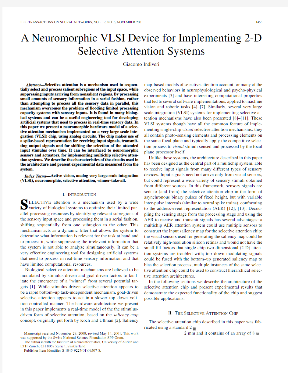
Fig.1.Schematic diagram of an AER chip to chip communication example:“slow”action potentials generated by the “many”(N)neurons of the source chip are transmitted as “fast”address events,on the “few”(log N )wires of the AE bus,to the synapses of the destination chip
neurons.
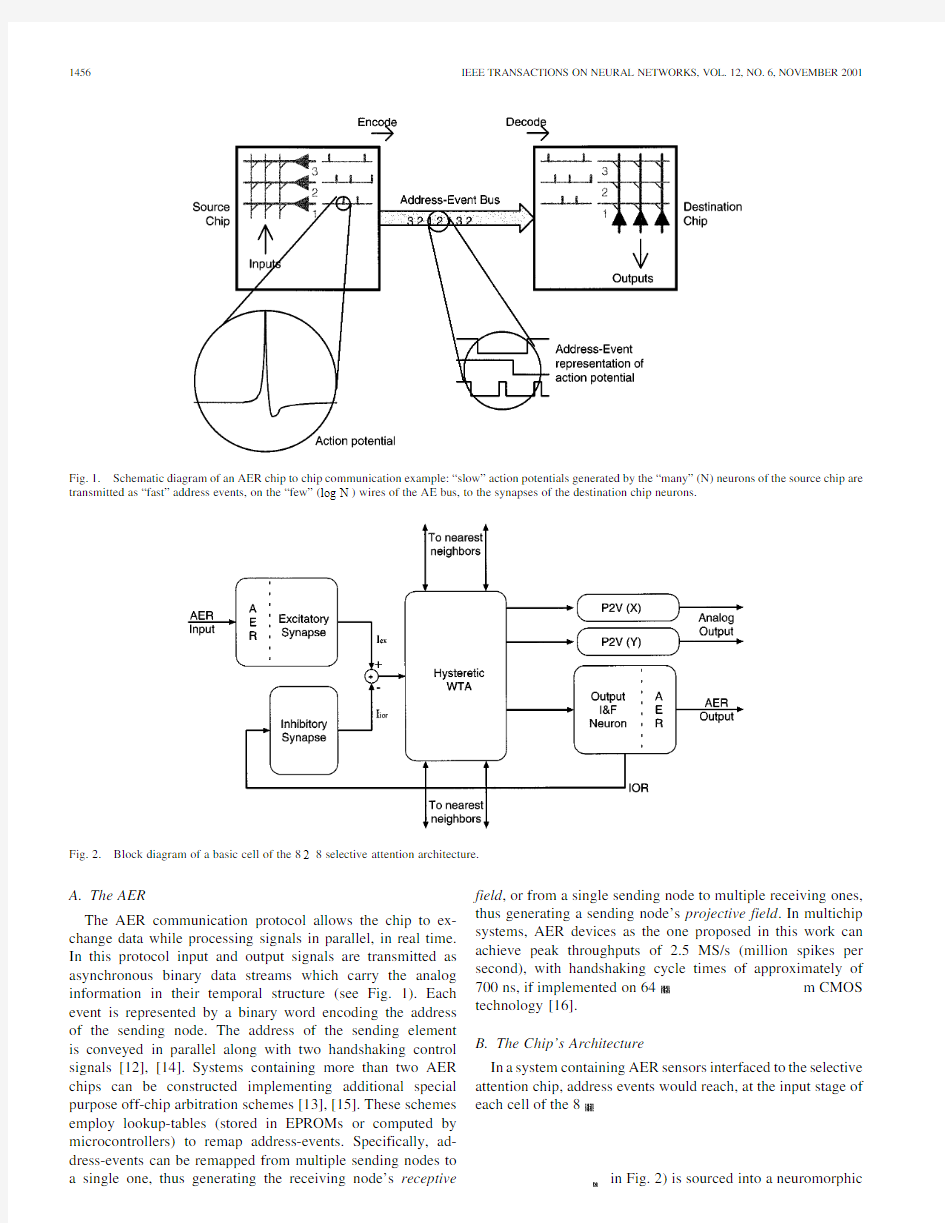
Fig.2.Block diagram of a basic cell of the 828selective attention architecture.
A.The AER
The AER communication protocol allows the chip to ex-change data while processing signals in parallel,in real time.In this protocol input and output signals are transmitted as asynchronous binary data streams which carry the analog information in their temporal structure (see Fig.1).Each event is represented by a binary word encoding the address of the sending node.The address of the sending element is conveyed in parallel along with two handshaking control signals [12],[14].Systems containing more than two AER chips can be constructed implementing additional special purpose off-chip arbitration schemes [13],[15].These schemes employ lookup-tables (stored in EPROMs or computed by microcontrollers)to remap address-events.Specifically,ad-dress-events can be remapped from multiple sending nodes to a single one,thus generating the receiving node’s receptive
field ,or from a single sending node to multiple receiving ones,thus generating a sending node’s projective field .In multichip systems,AER devices as the one proposed in this work can achieve peak throughputs of 2.5MS/s (million spikes per second),with handshaking cycle times of approximately of
700ns,if implemented on
64
m CMOS technology [16].
B.The Chip’s Architecture
In a system containing AER sensors interfaced to the selective attention chip,address events would reach,at the input stage of each cell of the
8
in Fig.2)is sourced into a neuromorphic
INDIVERI:A NEUROMORPHIC VLSI DEVICE
1457
Fig.3.Synaptic circuits.(a)Input excitatory synapse.Address events are converted into pulses by the circuit in the dashed box.Pulses are integrated into the excitatory current I by the p-type current-mirror integrator.The integrator’s gain and time constant are modulated by the control voltages V
)are integrated into
the inhibitory current I
and V .
analog circuit that,connected with its neighbors,implements a hysteretic winner-take-all (WTA)network [17].The output current of each WTA cell is used to activate both an integrate and fire (I&F)neuron and two position to voltage (P2V)cir-cuits [18].The P2V circuits encode
the
coordinates of the winning WTA cell with two analog voltages,while the I&F neurons generate pulses that are used by the AER interfacing circuits to encode the position of the winning WTA cell with ad-dress-events.The neuron’s spikes are also integrated by the local inhibitory synapse connected to it,to generate a
current
(see Fig.2).Fig.3shows
the circuit diagram of both excitatory and inhibitory synapses.Both circuits use compact,nonlinear current-mirror integrators [16],[19]to integrate their input spikes.The transistors in the dashed box of Fig.3(a)implement the AER input interfacing circuits and can operate correctly over a wide range of input pulse widths,ranging from a few hundred nanoseconds to mil-liseconds[16].The gain and time constants of the two current-mirror integrators are set by two pairs of control voltages
(
for the excitatory synapse
and for the in-hibitory synapse).
The sum of the currents
(
in Fig.4(a)].Each
cell is connected to its four nearest neighbors,both with lateral excitatory connections and lateral inhibitory connections [see Fig.4(a)].The inhibitory connections are modulated by the bias
voltage
and control the spatial extent over which compe-tition takes place.If lateral inhibition is maximally turned on
(
),all WTA cells of the architecture are connected together and only one winner can be selected at a time (global in-hibition).
If
is low,the WTA network allows multiple win-ners to be selected,as long as they are sufficiently distant from each other (local inhibition).Similarly,lateral excitatory con-nections,modulated by the bias
voltage
increases above V is driven to V
and an address event is generated.The transistors in the dashed box are part of the output AER circuitry.
When a WTA cell is selected as a winner,its output transistors source dc currents into the two P2V row and column circuits.The winning WTA cell also sources a dc
current
1458IEEE TRANSACTIONS ON NEURAL NETWORKS,VOL.12,NO.6,NOVEMBER2001 inverters of Fig.4(b)drives to the positive power supply
rail.This activates the AER row and column request signals
(
.
Next to transmitting their address events off chip,the output
neurons,together with the local inhibitory synapse connected
to them,implement the inhibition of return(IOR)mechanism
(a key feature of many selective attention systems)[20],[21].
The spikes generated by the winning cell’s output neuron are
integrated by its corresponding inhibitory synapse and gradually
increase the cell’s inhibitory postsynaptic current
and
INDIVERI:A NEUROMORPHIC VLSI DEVICE
1459
Fig.6.Event histograms of addresses generated by the workstation sent to the chip(a)and output addresses generated by the selective attention chip(b),(c),and (d).All chip parameters are kept constant throughout the plots except for the bias parameter V.The histogram in(b)was obtained with V=227mV,the one in(c)with V=207mV and the one in(d)with V=193mV.
driving the P2V circuits and their outputs tend to drift toward zero.This is evident in Fig.5(a),for example,at the position corresponding to cell(7,2)in the lower right corner of the figure. When the network selects it as its eighth target,the horizontal P2V circuit outputs approximately4.4V and the vertical one outputs approximately1.3V.When the IOR mechanism forces the network to deselect the winner the outputs of the P2V cir-cuits slowly drift toward zero.As soon as inhibition decreases, the network selects the cell(7,7)as the new(ninth)winner,the position to voltage circuits are actively driven again and their output quickly changes from approximately3.6V and1.2V to 4.2V and3.5V(for the horizontal and vertical circuits,respec-tively).
B.Digital AER Outputs
To verify that the AER outputs are consistent with the analog P2V outputs,we stimulated the chip with the same pattern used for collecting the data of Fig.5(a).We measured the address-events generated by the selective attention chip in response to this input stimulus using a logic analyzer and plotted in Fig.5(b) the histogram of such events.As shown,the chip’s output ad-dress-events reflect,on average,the input stimulus and are con-sistent with the analog outputs of the P2V circuits.
The data of both Fig.5(a)and(b)demonstrate how the IOR mechanism forces the network to switch the selection of the winner from one input to a different one,cycling through all sufficiently strong inputs.To demonstrate also how different IOR dynamics settings[modified for example by changing the bias
voltage
.The data of Fig.6(b)was obtained by setting the time constant of the inhibitory synapse to a relatively high value
(mV).In this case once a cell is inhibited(after being selected as the winner),its input is sup-
1460IEEE TRANSACTIONS ON NEURAL NETWORKS,VOL.12,NO.6,NOVEMBER
2001
Fig.7.Output address events of the selective attention chip biased with V =207mV.The 2-D address space of the chip’s architecture is mapped into the plot’s one-dimensional ordinate vector by labeling each address successively,row by row.
pressed for an extensive period of time and the WTA network is forced to select all other (nonsuppressed)inputs.Conversely,the data of Fig.6(d)was obtained by setting synapse time con-stant to a relatively low value
(
mV).In this case the WTA network switches from selecting the cell receiving the strongest input to the cell receiving the second-strongest input and back.As the selected cells are not suppressed for sufficiently long periods of time,the remaining inputs never win the WTA competition.The histogram in Fig.6(c)shows the data obtained
for the intermediate case
of
mV.The same data used to compute the address-event histograms of Fig.6can be displayed using a different representation,to show the dynamics of the WTA competition stage.In Fig.7,we plotted the address-events measured for the intermediate case of Fig.6(c)over time.The addresses of the
8
and of Fig.4(a)],endow the
system with a sufficient amount of flexibility to be able to use the same chip in different types of selective attention tasks.
IV .S ELECTIVE A TTENTION A PPLICATIONS
The test stimuli used in the experiments of Section III were simple examples designed to demonstrate the expected
behavior
Fig.8.Image representations of saliency maps.(a)Saliency map corresponding to the input stimulus used for the experiment of Fig.5.(b)Saliency map used for the experiment of Fig. 6.(c)Fictitious example resembling a realistic saliency map.
of the selective attention chip.They do not resemble realistic saliency maps [see Fig.8(a)and (b)].In practical applications
INDIVERI:A NEUROMORPHIC VLSI DEVICE
1461 Fig.9.Selective attention active vision system.The selective attention chip processes sensory data coming from an AER imaging sensor and transmits its output to a workstation that drives the pan-tilt unit on which the sensor is mounted.A standard CCD camera is mounted next to the AER sensor to visualize the sensor’s filed of view.
saliency maps would more likely resemble the one shown in Fig.8(c).More elaborate saliency maps could be processed by 2-D selective attention networks of greater size.The
8 most salient regions of the image,or to scan the whole image in an intelligent way,sorting the scanning process by re-gion saliency.Depending on the chip’s bias settings,the system could also be tuned to visit each region only once,switching from region to the other slowly,or to revisit each region over and over again,switching from one region to the other quickly. Systems of this type would already benefit from the real-time response properties of the selective attention chip.But the most effective way of exploiting the computational properties of this chip would be to use it in conjunction with neuromorphic sen-sors that employ the AER communication protocol,such as sil-icon retinas or silicon cochleas[23]–[25].These types of sys-tems could be used as research tool for testing,in real-time, with real stimuli,different hypotheses on biological selective attention mechanisms[1],[26],[27].Or they could be used as low-cost alternatives to implement visual/auditory tracking or monitoring systems.For example,rather than using several fixed high-resolution(high-cost)cameras to monitor an environ-ment,one could use a single motorized high-resolution camera driven by a selective attention system,comprising an AER sil-icon retina with a wide-field of view lens interfaced to the se-lective attention chip.An active vision system of this type,de-scribed in detail in[28],is shown in Fig.9:the selective atten-tion chip receives input from an AER imaging sensor[24]and transmits the address of the winning pixel to a workstation,that is used to drive the pan-tilt unit on which the sensor is mounted.
A standard CCD camera is mounted next to the sensor,to vi-sualize the sensor’s field of view.The AER sensor responds to contrast transients and its address events report the position of moving objects.The selective attention chip selects the locations with highest contrast moving objects and cycles through them, while the workstation drives the pan-tilt unit centering the se-lected locations with the sensor’s imaging array.An example of behavior of such a system,in response to real-world stimuli is shown in Fig.10.The selective attention chip selects a moving target in the top-left part of the image and the pan-tilt unit is driven in a way to center the AER sensor’s imaging array with the location selected by the attention chip.
V.C ONCLUSION
We presented an analog VLSI device that implements a2-D neuromorphic model of selective attention,for sequentially se-lecting the most salient locations of its inputs space.The device accepts input signals in the form of address-events and trans-mits its output using the same AER representation.It contains also analog position-to-voltage output circuits that can be used for quickly assessing the position of the selected input or for driving actuators,such as dc motors or pan-tilt units.We showed
1462IEEE TRANSACTIONS ON NEURAL NETWORKS,VOL.12,NO.6,NOVEMBER
2001
Fig.10.Active vision system behavior,in response to moving stimuli.The image represents the CCD camera’s output.The outer frame superimposed on the image represents the AER sensor’s field of view.The inner frame represents the center of the sensor’s imaging array and the cross represents the output of the selective attention chip.(a)Snapshot taken before the camera movement (the selective attention chip has just selected the moving stimulus in the top left part of the image).(b)Snapshot taken just after the the camera movement (the salient stimulus is now centered in the AER sensor’s imaging array).
experimental data that validates the functionality of the system,using control inputs generated on a workstation.We demon-strated how the chip’s bias parameters can be used to impose different behaviors of the system and suggested possible appli-cations.
The possibility to interface various types of AER sensory de-vices to the chip and to transmit the result of the selective at-tention competition to further processing stages using the same representation,allows the design of modular multichip selec-tive attention systems.In these multichip systems,the proper-ties of neuromorphic sensors,of the selective attention chip and of the AER ensure that the transduction of sensory signals,the selection of the most salient region and the implementation of the complex dynamics that characterize the selective attention
mechanism would all take place virtually in parallel and run in continuous and in real time.These features,together with the possibility to bias the system to exhibit different types of selec-tive attention behaviors,provide obvious advantages both for scientific investigation of selective attention system properties and for engineering applications.
A CKNOWLEDGMENT
The author would like to thank R.Douglas and K.Martin for their support,the MOSIS foundation for fabricating the VLSI chip,and A.Whatley and G.Chang for their comments on the manuscript.
R EFERENCES
[1] E.Niebur and C.Koch,“Computational architectures for attention,”in
The Attentive Brain ,R.Parasuraman,Ed.Cambridge,MA:MIT Press,1998,pp.163–186.
[2] C.Koch and S.Ullman,“Shifts in selective visual-attention—toward
the underlying neural circuitry,”Human Neurobiol.,vol.4,no.4,pp.219–227,1985.
[3]L.Itti and C.Koch,“Computational modeling of visual attention,”Na-ture Neurosci.Rev.,vol.2,pp.194–204,2001.
[4]L.Itti,C.Koch,and E.Niebur,“A model of saliency-based visual at-tention for rapid scene analysis,”IEEE Trans.Pattern Anal.Machine Intell.,vol.20,pp.1254–1259,Nov.1998.
[5]H.Bosch,https://www.doczj.com/doc/ff15224783.html,anese,and https://www.doczj.com/doc/ff15224783.html,bbi,“Object segmentation by attention-induced oscillations,”in Proc.IEEE Int.Joint Conf.Neural Networks ,vol.2,1998,pp.1167–1171.
[6]P.E.Trahanias,S.Velissaris,and T.Garavelos,“Visual landmark extrac-tion and recognition for autonomous robot navigation,”in Proc.IEEE Int.Conf.Intell.Robots Syst.IROS ’97,vol.2,1997,pp.1036–1043.[7]S.Baluja and D.A.Pomerleau,“Expectation-based selective attention
for the visual monitoring and control of a robot vehicle,”Robot.Au-tonomous Syst.J.,vol.22,pp.329–344,1997.
[8]V .Brajovic and T.Kanade,“Computational sensor for visual tracking
with attention,”IEEE J.Solid-State Circuits ,vol.33,pp.1199–1207,Aug.1998.
[9]T.K.Horiuchi and C.Koch,“Analog VLSI-based modeling of the pri-mate oculomotor system,”Neural Comput.,vol.11,pp.243–265,1999.[10]G.Indiveri,“Neuromorphic analog VLSI sensor for visual tracking:Cir-cuits and application examples,”IEEE Trans.Circuits Syst.II ,vol.46,pp.1337–1347,Nov.1999.
[11]T.G.Morris,T.K.Horiuchi,and S.P.DeWeerth,“Object-based selec-tion within an analog VLSI visual attention system,”IEEE Trans.Cir-cuits Syst.II ,vol.45,pp.1564–1572,Dec.1998.
[12]https://www.doczj.com/doc/ff15224783.html,zzaro,J.Wawrzynek,M.Mahowald,M.Sivilotti,and D.Gille-spie,“Silicon auditory processors as computer peripherals,”IEEE Trans.Neural Networks ,vol.4,pp.523–528,1993.
[13]S.R.Deiss,R.J.Douglas,and A.M.Whatley,“A pulse-coded commu-nications infrastructure for neuromorphic systems,”in Pulsed Neural Networks ,W.Maass and C.M.Bishop,Eds.Cambridge,MA:MIT Press,1998,ch.6,pp.157–178.
[14]K. A.Boahen,“Multiple pathways:Retinomorphic chips that see
quadruple images,”in Proc.7th Int.Conf.Microelectron.Neural,Fuzzy,Bio-Inspired Syst.;Microneuro’99,Los Alamitos,CA,Apr.1999,pp.12–20.
[15] C.Higgins and C.Koch,“Multichip motion processing,”in Proc.Conf.
Advanced Res.VLSI ,Atlanta,GA,1998.
[16]K.A.Boahen,“Communicating neuronal ensembles between neuro-morphic chips,”in Neuromorphic Systems Engineering ,https://www.doczj.com/doc/ff15224783.html,nde,Ed.Norwell,MA:Kluwer,1998,pp.229–259.
[17]G.Indiveri,“A current-mode analog hysteretic winner-take-all network,
with excitatory and inhibitory coupling,”J.Analog Integrated Circuits Signal Processing,2001.
[18]S.P.DeWeerth,“Analog VLSI circuits for stimulus localization and cen-troid computation,”https://www.doczj.com/doc/ff15224783.html,put.Vision ,vol.8,no.3,pp.191–202,1992.
[19]G.Indiveri,“Modeling selective attention using a neuromorphic analog
VLSI device,”Neural Comput.,vol.12,no.12,pp.2857–2880,Dec.2000.
INDIVERI:A NEUROMORPHIC VLSI DEVICE1463
[20] B.Gibson and H.Egeth,“Inhibition of return to object-based and en-
vironment-based locations,”in Percept.Psychopys.,1994,vol.55,pp.
323–339.
[21]Y.Tanaka and S.Shimojo,“Location vs feature:Reaction time reveals
dissociation between two visual functions,”Vision Res.,vol.36,no.14, pp.2125–2140,July1996.
[22] A.L.Yarbus,Eye Movements and Vision.New York:Plenum,1967.
[23]K.A.Boahen,“A retinomorphic vision system,”IEEE Micro,vol.16,
no.5,pp.30–39,Oct.1996.
[24]J.Kramer,An Integrated Optical Transient Sensor,2001,submitted for
publication.
[25] E.Fragnière,A.van Schaik,and E.Vittoz,“Design of an analogue VLSI
model of an active cochlea,”J.Analog Integrated Circuits Signal Pro-cessing,vol.13,no.1/2,pp.19–35,May1997.
[26]R.Desimone and J.Duncan,“Neural mechanisms of selective visual
attention,”Annu.Rev.Neurosci.,vol.18,pp.193–222,1995.
[27]M.C.Mozer and M.Sitton,“Computational modeling of spatial at-
tention,”in Attention,H.Pashler,Ed.East Sussex,U.K.:Psychology Press,1998,pp.341–395.
[28]G.Indiveri,R.Mürer,and J.Kramer,“Active vision using an analog
VLSI model of selective attention,”IEEE Trans.Circuits Syst.II,vol.
48,pp.492–500,May
2001.
Giacomo Indiveri received the Laurea degree in
electrical engineering from the University of Genoa,
Italy,in1992and won a postgraduate fellowship
within the“National Research Program on Bioelec-
tronic Technologies”from which he graduated(cum
laude)in1995.
From1994to1996,he worked as a Postdoctoral
Fellow in the Department of Biology at the California
Institute of Technology,Pasadena,working on the de-
sign of analog VLSI subthreshold neuromorphic ar-
chitectures for low-level visual tasks and motion de-tection.He is a Research Assistant at the Institute Neuroinformatics of the Swiss Federal Institute of Technology and the University of Zurich,Switzerland.His current research interests include the design and implementation of neuromor-phic systems for modeling selective attention neural mechanisms and for ex-ploring the computational properties of networks of silicon integrate and fire neurons.He is co-teacher of two classes on the analysis and design of analog VLSI Neuromorphic Systems at the Swiss Federal Institute of Zurich and co-or-ganizer of the Workshop Neuromorphic Engineering,held annually in Telluride, CO.
第三章、器件 一、超深亚微米工艺条件下MOS 管主要二阶效应: 1、速度饱和效应:主要出现在短沟道NMOS 管,PMOS 速度饱和效应不显著。主要原因是 TH G S V V -太大。在沟道电场强度不高时载流子速度正比于电场强度(μξν=) ,即载流子迁移率是常数。但在电场强度很高时载流子的速度将由于散射效应而趋于饱和,不再随电场 强度的增加而线性增加。此时近似表达式为:μξυ=(c ξξ<),c s a t μξυυ==(c ξξ≥) ,出现饱和速度时的漏源电压D SAT V 是一个常数。线性区的电流公式不变,但一旦达到DSAT V ,电流即可饱和,此时DS I 与GS V 成线性关系(不再是低压时的平方关系)。 2、Latch-up 效应:由于单阱工艺的NPNP 结构,可能会出现VDD 到VSS 的短路大电流。 正反馈机制:PNP 微正向导通,射集电流反馈入NPN 的基极,电流放大后又反馈到PNP 的基极,再次放大加剧导通。 克服的方法:1、减少阱/衬底的寄生电阻,从而减少馈入基极的电流,于是削弱了正反馈。 2、保护环。 3、短沟道效应:在沟道较长时,沟道耗尽区主要来自MOS 场效应,而当沟道较短时,漏衬结(反偏)、源衬结的耗尽区将不可忽略,即栅下的一部分区域已被耗尽,只需要一个较小的阈值电压就足以引起强反型。所以短沟时VT 随L 的减小而减小。 此外,提高漏源电压可以得到类似的效应,短沟时VT 随VDS 增加而减小,因为这增加了反偏漏衬结耗尽区的宽度。这一效应被称为漏端感应源端势垒降低。
4、漏端感应源端势垒降低(DIBL): VDS增加会使源端势垒下降,沟道长度缩短会使源端势垒下降。VDS很大时反偏漏衬结击穿,漏源穿通,将不受栅压控制。 5、亚阈值效应(弱反型导通):当电压低于阈值电压时MOS管已部分导通。不存在导电沟道时源(n+)体(p)漏(n+)三端实际上形成了一个寄生的双极性晶体管。一般希望该效应越小越好,尤其在依靠电荷在电容上存储的动态电路,因为其工作会受亚阈值漏电的严重影响。 绝缘体上硅(SOI) 6、沟长调制:长沟器件:沟道夹断饱和;短沟器件:载流子速度饱和。 7、热载流子效应:由于器件发展过程中,电压降低的幅度不及器件尺寸,导致电场强度提高,使得电子速度增加。漏端强电场一方面引起高能热电子与晶格碰撞产生电子空穴对,从而形成衬底电流,另一方面使电子隧穿到栅氧中,形成栅电流并改变阈值电压。 影响:1、使器件参数变差,引起长期的可靠性问题,可能导致器件失效。2、衬底电流会引入噪声、Latch-up、和动态节点漏电。 解决:LDD(轻掺杂漏):在漏源区和沟道间加一段电阻率较高的轻掺杂n-区。缺点是使器件跨导和IDS减小。 8、体效应:衬底偏置体效应、衬底电流感应体效应(衬底电流在衬底电阻上的压降造成衬偏电压)。 二、MOSFET器件模型 1、目的、意义:减少设计时间和制造成本。 2、要求:精确;有物理基础;可扩展性,能预测不同尺寸器件性能;高效率性,减少迭代次数和模拟时间 3、结构电阻:沟道等效电阻、寄生电阻 4、结构电容: 三、特征尺寸缩小 目的:1、尺寸更小;2、速度更快;3、功耗更低;4、成本更低、 方式: 1、恒场律(全比例缩小),理想模型,尺寸和电压按统一比例缩小。 优点:提高了集成密度 未改善:功率密度。 问题:1、电流密度增加;2、VTH小使得抗干扰能力差;3、电源电压标准改变带来不便;4、漏源耗尽层宽度不按比例缩小。 2、恒压律,目前最普遍,仅尺寸缩小,电压保持不变。 优点:1、电源电压不变;2、提高了集成密度 问题:1、电流密度、功率密度极大增加;2、功耗增加;3、沟道电场增加,将产生热载流子效应、速度饱和效应等负面效应;4、衬底浓度的增加使PN结寄生电容增加,速度下降。 3、一般化缩小,对今天最实用,尺寸和电压按不同比例缩小。 限制因素:长期使用的可靠性、载流子的极限速度、功耗。
数字信号处理的应用与发展趋势 作者:王欢 天津大学信息学院电信三班 摘要: 数字信号处理是应用于广泛领域的新兴学科,也是电子工业领域发展最为迅速的技术之一。本文就数字信号处理的方法、发展历史、优缺点、现代社会的应用领域以及发展前景五个方面进行了简明扼要的阐述。 关键词: 数字信号处理发展历史灵活稳定应用广泛发展前景 数字信号处理的简介 1.1、什么是数字信号处理 数字信号处理简称DSP,英文全名是Digital Signal Processing。 数字信号处理是利用计算机或专用处理设备以数字的形式对信号进行采集、变换、滤波、估值、增强、压缩、识别等处理,以得到符合人们需要的信号形式。 DSP系统的基本模型如下: 数字信号处理是一门涉及许多学科且广泛应用于许多领域的新兴学科。它以众多的学科为理论基础,所涉及范围及其广泛。例如,在数学领域、微积分、概率统计、随即过程、数值分析等都是数字信号处理的基本工具;同时与网络理论、信号与系统、控制论、通信理论、故障诊断等学科也密切相关。近年来的一些新兴学科,如人工智能、模式识别、神经网络等,都是与数字信号处理密不可分的。数字信号处理可以说许多经典的理论体系作为自己的理论基础,同时又使自己成为一门新兴学科的理论基础。 1.2、数字信号系统的发展过程 数字信号处理技术的发展经历了三个阶段。 70 年代DSP 是基于数字滤波和快速傅里叶变换的经典数字信号处理, 其系统由分立的小规模集成电路组成, 或在通用计算机上编程来实现DSP 处理功能, 当时受到计算机速度和存储量的限制,一般只能脱机处理, 主要在医疗电子、生物电子、应用地球物理等低频信号处理方面获得应用。 80 年代DSP 有了快速发展, 理论和技术进入到以快速傅里叶变换(FFT) 为主体的现代信号处理阶段, 出现了有可编程能力的通用数字信号处理芯片, 例如美国德州仪器公司(TI公司) 的TMS32010 芯片, 在全世界推广应用, 在雷达、语音通信、地震等领域获得应用, 但芯片价格较贵, 还不能进 入消费领域应用。 90 年代DSP 技术的飞速发展十分惊人, 理论和技术发展到以非线性谱估计为代表的更先进的信号处理阶段, 能够用高速的DSP 处理技术提取更深层的信息, 硬件采用更高速的DSP 芯片, 能实时地完成巨大的计算量, 以TI 公司推出的TMS320C6X 芯片为例, 片内有两个高速乘法器、6 个加法器, 能以200MHZ 频率完成8 段32 位指令操作, 每秒可以完成16 亿次操作, 并且利用成熟的微电子工艺批量生产,使单个芯片成本得以降低。并推出了C2X 、C3X 、C5X 、C6X不同应用范围的系列, 新一代的DSP 芯片在移动通信、数字电视和消费电子领域得到广泛应用, 数字化的产品性能价 格比得到很大提高, 占有巨大的市场。 1.3、数字信号处理的特点
《DSP技术与应用---基于TMS320C54X》 实验指导书 湘潭大学信息工程学院 姚志强 2010.09.23
TMS320VC5402 DSK使用注意事项 1) 先用并口电缆和串口线(用到的话)将TMS320VC5402DSK与PC机相连, 而后再将电源接上,打开Code Composer Studio(简称CCS)后有可能报TMS320VC5402DSK和PC机未能连上的错误,可在PC机的CMOS_BIOS重新设置并行口的特性。 2) 将TMS320VC5402DSK上的DIP Switches的5、6置ON,其它置OFF。 3) 要在关闭CCS后及在断电的情况下插拔USB电缆线和串口线。 4) 强烈建议不要带电插拨串口,插拨时至少有一端是断电的,否则串口容 易损坏。 5) TMS320VC5402DSK电路板上大多是CMOS集成电路,为防止静电击毁, 在拿出实验电缆后请立即将玻璃盖复原,任何时候都请不要用手及其它带电物体直接和电路板接触。 实验报告的撰写 1) 每个实验都单独写实验报告。 2) 实验要求和目的; 3) 实验主要内容; 4) 看懂程序代码,并画出程序流程图; 5) 作出硬件描述(如果与DSK板硬件有关); 6)实验结果和心得。 实验注意事项 1) 实验项目所建工程文件统一放在F:\TI\CCS\myprojects下,其余盘在重启后会复原。 2) 实验过程中,不要涉及到中文路径(CCS不支持),包括CCS程序安装路径、文件添加路径、实验源文件名称等。 3) 实验七CODEC语音回放实验用到DSK板,需要自带耳麦,请准备好。
实验一 CCS的安装与CCS操作界面的熟悉 一、实验目的 学会安装与设置Code Composer Studio。 熟悉CCS软件的操作界面。 二、实验设备 CCS安装光盘(本次安装程序在D:\DSP\ccs2.0ForC5000)、装有Windows 98以上操作系统的PC机 三、实验内容及步骤 https://www.doczj.com/doc/ff15224783.html,S的安装 安装前需要卸载系统原来的C5000,进入控制面板进行卸载完毕后,再开始下面的步骤。 (1)找到CCS的安装软件,点击安装程序setup.exe,双击启动安装。安装完成后在 桌面上会有“CCS 2 C5000”和“SETUP CCS 2 C5000”两个快捷方式图标,分别对应CCS应用程序和CCS配置程序。 (2)双击运行“SETUP CCS 2 C5000”配置程序,配置驱动程序。本次实验没有用到实验箱,只需配置软件驱动程序。在弹出的“Import Configurantions”对话框中,先点击“Clear”键,清除以前的配置,然后选择“C5402 Simulator”,点击“Import”,最后点击“Save and Quit”按钮,完成配置。 https://www.doczj.com/doc/ff15224783.html,S操作界面的熟悉 (1)在桌面上双击“CCS 2 C5000”,弹出一个TI仿真器并行调试管理器窗口。 (2)在管理器窗口的“open”菜单下选择“C54xx(C5402) Simulator”命令,将弹出一个CCS运行主窗口(如果直接弹出CCS运行主窗口,此步可略)。 (3) 点击Help_>Contents打开TMS320C54x Code Composer Stdio Help,在左边Contents列表中点击最后一个TMS320C5402 DSK,浏览了解其下所有子列表的内容,熟悉DSK板的基本硬件、配置及功能。 (4)对照教材介绍CCS的地方,逐一熟悉CCS中的12项菜单的功能,包括File、Edit、View、Project、Debug、Profiler、Option、GEL、Tools等菜单(结合实验二建立项目熟悉更好)。 (5)对照教材,逐一熟悉CCS的五种工具栏:Standard Toolbar、GEL Toolbar、Project Toolbar、Debug Toolbar、Edit Toolbar(结合实验二建立项目熟悉更好)。
一种雷达通用信号处理系统的实现与应用 一种雷达通用信号处理系统的实现与应用 FPGA是一种现场可编程器件,设计灵活方便可以反复修改内部逻辑,适用于算法结构比较简单、处理速度较高的情况。DSP是一种基于指令集的处理器,适于大信息、复杂算法的信息处理场合。鉴于两种处理器件自身优势,FPGA+DSP信号处理架构,已成为信号处理系统的常用结构。但当前FPGA+DSP的信号处理平台或者是基于某些固定目的,实现某些固定功能,系统的移植性、通用性较差。或者仅仅简要介绍了平台的结构没有给出一些具体的实现。本文提出的基于FPGA+DSP通用信号处理平台具有两种处理器的优点,兼颐速度和灵活性,而且可以应用在不同雷达信号处理系统中,具有很强的通用性。本文举例说明该系统在连续波雷达和脉冲雷达中的典型应用。1系统资源概述1.1处理器介绍本系统FPGA选择Altera公司的EP2S60F1020。Stratix II FPGA采用TSMC的90nm 低k绝缘工艺技术。Stratix II FPGA支持高达1Gb·s-1的高速差分I/O信号,满足新兴接口包括LVDS,LNPECL和HyperTransport标准的高性能需求,支持各种单端I/O接口标准。EP2S60系列内部有48352个ALUT;具有2544192bit的RAM 块,其中M512RAM(512bit)329个,M4K RAM(4kbit)255个,M-RAM(512kbit)2个。具有嵌入式DSP块36个,等效18bit×18bit乘法器144个;具有加强型锁相环EPLL4个,
快速锁相环FPLL8个。这些锁相环具有高端功能包括时钟切换,PLL 重新配置,扩频时钟,频率综合,可编程相位偏移,可编程延迟偏移,外部反馈和可编程带宽等。本系统DSP选择ADI公司的ADSP TS201。它有高达600MHz的运行速度,1.6ns的指令周期;有24MB的片内DRAM;双运算模块,每个计算块包含1个ALU,一个乘法器,1个移位器,1个寄存器组和1个通信逻辑单元(CLU);双整数ALU,提供数据寻址和指针操作功能;集成I/O接口,包括14通道的DMA控制器,外部端口,4个链路口,SDRAM控制器,可编程标识引脚,2个定时器和定时器输出引脚等用于系统连接;IEEE1149.1兼容的JTAG端口用于在线仿真;通过共享总线可以无缝连接多达8个TigerSHARC DSP。1.2FPGA+DSP结构由于FPGA和DSP各自的自身优势,FPGA+DSP信号处理架构已成为信号处理系统的常用结构。一般情况下FPGA+DSP的拓扑结构会根据需要进行不同的连接,这就导致这种结构的专用性,缺乏灵活性。对于一个通用处理平台要考虑到各种不同的信号通路,因此大部分通用FPGA+DSP平台都采取各个处理器间均有通路的方式。这种拓扑结构灵活方便,可以满足各种不同的通路需求,这种结构的缺点就是硬件设计的复杂以及可能会有资源浪费。对于这种通用FPGA+DSP 结构,FPGA与各个DSP之间均有连接,不同之处便是DSP之间的拓扑结构。一般分两种,一是高速外部总线口耦合结构组成多DSP 系统,这种结构可以实现多DSP共享系统内的资源,系统内的个处理器可以共享RAM,SDRAM和主机等资源,还可共享其他处理器核
由于成本、系统功耗和面市时间等原因,许多通讯、视频和图像系统已无法简单地用现有DSP处理器来实现,现场可编程门阵列(FPGA)尤其适合于乘法和累加(MAC)等重复性的DSP任务。本文从FPGA与专用DSP器件的运算速度和器件资源的比较入手,介绍FPGA 在复数乘法、数字滤波器设计和FFT等数字信号处理中应用的优越性,值得(中国)从事信号处理的工程师关注。 Chris Dick Xilinx公司 由于在性能、成本、灵活性和功耗等方面的优势,基于FPGA的信号处理器已广泛应用于各种信号处理领域。近50%的FPGA产品已进入各种通信和网络设备中,例如无线基站、交换机、路由器和调制解调器等。FPGA提供了极强的灵活性,可让设计者开发出满足多种标准的产品。例如,万能移动电话能够自动识别GSM、CDMA、TDMA或AMPS等不同的信号标准,并可自动重配置以适应所识别的协议。FPGA所固有的灵活性和性能也可让设计者紧跟新标准的变化,并能提供可行的方法来满足不断变化的标准要求。 复数乘法 复数运算可用于多种数字信号处理系统。例如,在通讯系统中复数乘积项常用来将信道转化为基带。在线缆调制解调器和一些无线系统中,接收器采用一种时域自适应量化器来解决信号间由于通讯信道不够理想而引入的干扰问题。量化器采用一种复数运算单元对复数进行处理。用来说明数字信号处理器优越性能的指标之一就是其处理复数运算的能力,尤其是复数乘法。 一个类似DSP-24(工作频率为100MHz)的器件在100ns内可产生24×24位复数乘积(2个操作数的实部和虚部均为24位精度)。复数乘积的一种计算方法需要4次实数乘法、1次加法和1次减法。一个满精度的24×24实数管线乘法器需占用348个逻辑片。将4个实数乘法器产生的结果组合起来所需的2个48位加法/减法器各需要24个逻辑片(logic slice)。这些器件将工作在超过100MHz的时钟频率。复数乘法器采用一条完全并行的数据通道,由4×348+2×24=1440个逻辑片构成,这相当于Virtex XCV1000 FPGA所提供逻辑资源的12%。计算一个复数乘积所需的时间为10ns,比DSP结构的基准测试快一个数量级。为了获得更高的性能,几个完全并行的复数乘法器可在单个芯片上实现。采用5个复数乘法器,假设时钟频率为100MHz,则计算平均速率为每2ns一个复数乘积。这一设计将占用一个XCV1000器件约59%的资源。 这里应该强调的一个问题是I/O,有这样一条高速数据通道固然不错,但为了充分利用它,所有的乘法器都须始终保持100%的利用率。这意味着在每一个时钟来临时都要向这些单元输入新的操作数。 除了具有可实现算法功能的高可配置逻辑结构外,FPGA还提供了巨大的I/O带宽,包括片上和片外数据传输带宽,以及算术单元和存储器等片上部件之间的数据传输带宽。例如,XCV1000具有512个用户I/O引脚。这些I/O引脚本身是可配置的,并可支持多种信号标准。实现复数乘法器的另一种方法是构造一个单元,该单元采用单设定或并行的24x24实数乘法器。这种情况下,每一个复数乘法需要4个时钟标识,但是FPGA的逻辑资源占用率却降到了最低。同样,采用100MHz系统时钟,每隔40ns可获得一个新的满精度复数乘积,这仍是DSP结构基准测试数据的2.5倍。这一设定方法需要大约450个逻辑片,占一个XCV1000器件所有资源的3.7%(或XCV300的15%)。 构造一条能够精确匹配所需算法和性能要求的数据通道的能力是FPGA技术独特的特性之一。而且请注意,由于FPGA采用SRAM配置存储器,只需简单下载一个新的配置位流,同样的FPGA硬件就可适用于多种应用。FPGA就像是具有极短周转时间的微型硅片加工厂。
雷达数字信号处理解决方案 1.背景 数字信号处理是现代通信、雷达和电子对抗设备的重要组成部分。在实际应用中,利用数字信号处理技术对接收数据进行处理,不仅可以实现高精准的目标定位和目标跟踪,还能够将目标识别、目标成像、精确制导、电子对抗等功能进行拓展,实现多种业务的一体化集成。 在现代雷达系统中,随着有源相控阵和数字波束形成(DBF)技术的广泛应用,接收前端存在大量的数据需要并行处理,并需要保证高性能和低延迟的特点。雷达日益复杂的应用环境,让雷达系统具备自适应于探测目标和环境的能力,数字信号处理部分也需要使用多种更加复杂的算法,并且可以做到算法模块化,以及通过软件配置功能模块的参数,实现软件定义的功能。更大的数据处理带宽能够使雷达获得更高的分辨率,更高的工作频率使得雷达可以小型化,能够在更小的平台上安装,这样对于硬件平台实现也有低功耗的要求。 在电子对抗设备中,可以在最短的时间内对多个威胁目标进行快速分析和响应,同样需要数字信号处理的相关算法具备高实时,高动态范围和自适应的特点。如何在宽频噪声的环境中寻找到目标的特征数据,如何在宽带范围内制造虚假目标实现全覆盖,数字信号的处理性能是至关重要的设计因素。 加速云的SC-OPS和SC-VPX产品,针对5G通信和雷达的数字信号处理的要求,结合Intel最新14nm 工艺的Stratix10 FPGA系列,提供了一套完整的硬件和软件相结合的解决方案。SC-OPS产品作为单独的硬件加速卡,通过PCIe插卡的方式实现与主机的通信功能,还可以通过多卡级联的方式实现数字信号的分布式处理方案。SC-VPX产品是由FPGA业务单板、主控板和机箱组成的VPX系统。借助于FPGA可编程的特性,加速云提供了高性能数学加速库FBLAS和FFT的RTL级IP,具有高性能和算法参数可配置的特点实现了多重信号分类(MUSIC)和自适应数字波束形成(ADBF)的核心算法,提高了5G通信和雷达在对抗干扰方面的性能。为了方便客户使用高层语言开发,加速云提供基于FPGA完整的OpenCL异构开发环境,快速实现用户自定义的信号处理加速方案。 图1. 加速云SC-OPS和SC-VPX产品
基于TMS320C6455的高速数字信号处理系统设计 摘要:针对高速实时数字信号处理系统设计要求,本文提出并设计了基于dsp+fpga结构的高速数字信号处理系统,采用ti公司目前单片处理能力最强的定点dsp芯片tms320c6455为系统主处理器,fpga作为协处理器。详细论述了dsp外围接口电路的应用和设计,系统设计电路简洁、实现方便,可靠性强。 关键词:tms320c6455 fpga 数字信号处理系统设计 design of high-speed digital signal processing system based on tms320c6455 cao jingzhi,he fei,li qiang,ren hui,qin wei (department of tool development,china petroleum logging co.,ltd shaan xi xi’an 710077) abstract:according to the design needs of high-speed real-time digital signal processing system.the paper puts forward a design of high-speed digital signal processing system based on dsp+fpga structure,adopting ti company fixed-point dsp chip tms320c6455,the currently strongest capacity monolithic processor,for system main processor,and fpga as coprocessor.this paper describs the application and design of dsp periphery circuit interface in detail.the system design has simple circuit and realize convenient, reliability.
2002 年版权,复旦大学专用集成电路与系统国家重点实验室(设计流程1) 数字集成电路设计流程介绍 唐长文 2002年7月8日
2002 年版权,复旦大学专用集成电路与系统国家重点实验室(设计流程2) 内容 一、设计流程介绍1、流程图及设计步骤2、EDA软件 二、硬件描述语言简介 1、传统自下向上的设计方法 2、基于硬件描述语言的自顶向下的设计方法 3、硬件描述语言--VHDL介绍 4、VHDL语言设计实例 三、数字系统的结构设计-行为级或RTL级设计1、系统规范2、系统框架 3、系统源代码设计 4、系统行为级仿真 四、数字系统的电路设计--门级电路设计1、FPGA逻辑综合2、ASIC逻辑综合3、综合后仿真 五、数字系统的版图设计1、FPGA器件实现 2、基于标准单元ASIC版图的自动化生成 3、版图后仿真 六、版图验证和管子级仿真1、DRC&LVS 2、Star_sim管子级仿真
一、设计流程介绍 C语言仿真Matlab仿真COSSAP仿真
2002 年版权,复旦大学专用集成电路与系统国家重点实验室(设计流程4) 数字集成电路设计主要分为四大步:1、行为级、RTL 级源代码设计2、电路设计-门级电路设计(1)FPGA 逻辑综合(2)ASIC 逻辑综合3、版图设计 (1)FPGA 版图布局布线设计(器件实现) (2)ASIC 版图布局布线设计(基于标准单元库)4、版图验证(DRC&LVS) ?设计的步骤
2002 年版权,复旦大学专用集成电路与系统国家重点实验室 (设计流程5) ?EDA 软件 (1)FPGA 设计需要的软件源代码设计和仿真9Active-HDL FPGA 逻辑综合 9Synopsys FPGA Express 、Synplicity Synplify 、 Examplar LeonardoSpectrum 、XST(Xilinx Synthesis Tech)FPGA 器件实现 9Xilinx Foundation ISE 、Altera MaxplusII
课程设计题目:常用基本数字集成电路应用设计 学生姓名: 学号: 院系: 专业班级: 指导教师姓名及职称: 起止时间: 课程设计评分: 常用基本数字集成电路应用设计 1.多谐振荡器概述 多谐振荡器是一种自激振荡器,它不需要输入触发信号,接通电源后就可自动输出矩形脉冲。由于矩形脉冲含有丰富的谐波分量,因此,常将矩形脉冲产生电路称为多谐振荡器。 1.1非门电路构成的多谐振荡器设计
1.1.1基本原理 门电路构成多谐振荡器 非门作为一个开关倒相器件,可用以构成各种脉冲波形的产生电路。电路的基本工作 原理是利用电容器的充放电,当输入电压达到与非门的阈值电压VT 时,门的输出状态即发生变化。因此,电路输出的脉冲波形参数直接取决于电路中阻容元件的数值。 (1)不对称多谐振荡器 非对称型多谐振荡器的输出波形是不对称的,当用TTL与非门组成时,输出脉冲宽度 tw1=RC, tw2=1.2RC, T=2.2RC 调节 R和C值,可改变输出信号的振荡频率,通常用改变C实现输出频率的粗调,改 变电位器R实现输出频率的细调。 图1为不对称多谐振荡器,为了使电路产生振荡,要求U1A和U1B两个反向器都工作在电压传输特性的转折区,即工作在放大区。 (2)对称型多谐振荡器 电路完全对称,电容器的充放电时间常数相同, 故输出为对称的方波。改变R和C的值, 可以改变输出振荡频率。非门3用于输出波形整形。 一般取R≤1KΩ?,当R1=R2=1KΩ,C1=C2=100pf~100μf时,f可在几Hz~MHz 变化。
脉冲宽度tw1=tw2=0.7RC,T=1.4RC. 图2中,U1A和U1B两个反向器之间经电容C1和C2耦合形成正反馈回路。 (3) 石英晶体稳频的多谐振荡器 当要求多谐振荡器的工作频率稳定性很高时,上述几种多谐振荡器的精度已不能满足要 求。为此常用石英晶体作为信号频率的基准。用石英晶体与门电路构成的多谐振荡器常用来 为微型计算机等提供时钟信号。 图3所示为常用的晶体稳频多谐振荡器。(a)、 (b)为TTL器件组成的晶体振荡电路;(c)、 (d)为CMOS器件组成的晶体振荡电路,一般用于电子表中,其中晶体的f0=32768Hz。 图3(c)中,门1用于振荡,门2用于缓冲整形。Rf是反馈电阻,通常在几十兆欧之 间选取,一般选22MΩ。R起稳定振荡作用,通常取十至几百千欧。C1是频率微调电容器, C2用于温度特性校正。
西安工程大学学报 Journal of Xi’an Polytechnic University 第22卷第3期(总91期)2008年6月Vol.22,No.3(Sum.No.91) 文章编号:16712850X(2008)0320329204 测速雷达数字信号处理系统的设计 张雪侠1,党幼云1,杨 进2 (1.西安工程大学电子信息学院,陕西西安710048;2.西安展意信息科技有限公司,陕西西安710075) 摘要:采用PCI29812数据采集卡和XC2S200FP GA芯片共同完成测速雷达系统的信号处理,即高速A/D转换模块和频谱的分析,并利用VB语言实现速度时间曲线的拟合问题和终端界面的显示,完成友好的人机交互功能. 关键词:测速雷达;信号处理系统;PCI29812采集卡;界面显示 中图分类号:TN911.25 文献标识码:A 0 引 言 传统的测试速度技术,如靶圈测试、天幕靶测试等方法因测试过程繁琐,精度较差,已不能满足实时战地测试的需要[1].连续波雷达回波的多普勒频移测量方法,具有测速精度高,无速度模糊[2],并且可以得到单值无模糊的频率值[3]的特点,单对于测速来说,是最理想的方法.对于雷达后端信号处理部分,根据实际要求的不同,存在有不同的处理方法[427].目前,实际应用中存在多种车载雷达测速仪,它主要是测量出运动目标的即时速度并进行记录与显示,因而对于终端信号处理相对比较简单.本文设计的测速雷达数字信号处理系统不仅能完成弹丸速度的实时测量、记录与显示,更重要的是通过弹丸速度的连续测定,进而获取弹丸初速值.弹丸初速值的确定对于计算弹道的相关参数,分析弹丸的形状及大小具有重要的意义. 1 测速雷达系统组成 1.1 基本原理 连续波测速雷达系统的理论基础是多普勒效应[4]在电磁波领域中的应用.其基本原理是雷达中的波震荡器震荡出一系列的波,通过天线向着飞行中的弹丸发射电磁波,同时接收弹丸的反射回波,由于弹丸在运动,所以反射波和接收波之间存在有频率差,即发生了频率的变化,就是所谓的频移现象.这一频率差和弹丸的运动速度成正比例关系.其数学表达式为多普勒频差f d=2V t/λ,式中λ为信号波长,V t为运动目标的即时速度;λ=c/f0,c为光速,为常量,由于雷达发射的频率f0已知,可求出λ,那么只要再求出多普勒信号的频率差值f d,即可求得弹丸的即时速度V t.由于得到的是连续的f d的值,即对应多个V t值,因此可得出弹丸飞行轨迹上的多点瞬时速度值,即弹丸速度变化曲线,再根据此曲线按最小二乘法进行拟合,推算出弹丸的初速V o值. 1.2 整体结构 测速雷达由信号采集机和信号处理机组成,其中信号采集机包括高频组件、喇叭天线、前置放大器、红外启动器;信号处理机包括数字信号处理器和终端显示界面. 信号采集机部分完成了雷达发射机和部分接收机的功能.8mm波振荡器产生连续的8mm电磁波,通 收稿日期:2008204211 通讯作者:党幼云(19622),女,陕西省澄城县人,西安工程大学教授.E2mail:xk_dyy@https://www.doczj.com/doc/ff15224783.html,
《数字信号处理》课程教学大纲 课程编号: 11322617,11222617,11522617 课程名称:数字信号处理 英文名称:Digital Signal Processing 课程类型: 专业核心课程 总学时:56 讲课学时:48 实验学时:8 学分:3 适用对象: 通信工程专业、电子信息科学与技术专业 先修课程:信号与系统、Matlab语言及应用、复变函数与积分变换 执笔人:王树华审定人:孙长勇 一、课程性质、目的和任务 《数字信号处理》是通信工程、电子信息科学与技术专业以及电子信息工程专业的必修课之一,它是在学生学完了信号与系统的课程后,进一步学习其它专业选修课的专业平台课程。本课程将通过讲课、练习、实验使学生掌握数字信号处理的基本理论和方法。为以后进一步学习和研究奠定良好的基础。 二、课程教学和教改基本要求 数字信号处理是用数字或符号的序列来表示信号,通过数字计算机去处理这些序列,提取其中的有用信息。例如,对信号的滤波,增强信号的有用分量,削弱无用分量;或是估计信号的某些特征参数等。总之,凡是用数字方式对信号进行滤波、变换、增强、压缩、估计和识别等都是数字信号处理的研究对象。 本课程介绍了数字信号处理的基本概念、基本分析方法和处理技术。主要讨论离散时间信号和系统的基础理论、离散傅立叶变换DFT理论及其快速算法FFT、IIR和FIR数字滤波器的设计以及有限字长效应。通过本课程的学习使学生掌握利用DFT理论进行信号谱分析,以及数字滤波器的设计原理和实现方法,为学生进一步学习有关信息、通信等方面的课程打下良好的理论基础。 本课程将通过讲课、练习、实验使学生掌握数字信号处理的基本理论和方法。为以后进一步学习和研究奠定良好的基础,应当达到以下目标: 1、使学生建立数字信号处理系统的基本概念,了解数字信号处理的基本手段以及数字信号处理所能够解决的问题。 2、掌握数字信号处理的基本原理,基本概念,具有初步的算法分析和运用MATLAB编程的能力。 3、掌握数字信号处理的基本分析方法和研究方法,使学生在科学实验能力、计算能力和抽象思维能力得到严格训练,培养学生独立分析问题与解决问题的能力,提高科学素质,为后续课程及从事信息处理等方面有关的研究工作打下基础。 4、本课程的基本要求是使学生能利用抽样定理,傅立叶变换原理进行频谱分析和设计简单的数字滤波器。 三、课程各章重点与难点、教学要求与教学内容
数字IC设计流程及工具介绍 IC的设计过程可分为两个部分,分别为:前端设计(也称逻辑设计)和后端设计(也称物理设计),这两个部分并没有统一严格的界限,凡涉及到与工艺有关的设计可称为后端设计。 前端设计的主要流程: 1、规格制定 芯片规格,也就像功能列表一样,是客户向芯片设计公司(称为Fabless,无晶圆设计公司)提出的设计要求,包括芯片需要达到的具体功能和性能方面的要求。 2、详细设计 Fabless根据客户提出的规格要求,拿出设计解决方案和具体实现架构,划分模块功能。 3、HDL编码 使用硬件描述语言(VHDL,Verilog HDL,业界公司一般都是使用后者)将模块功能以代码来描述实现,也就是将实际的硬件电路功能通过HDL语言描述出来,形成RTL(寄存器传输级)代码。 4、仿真验证 仿真验证就是检验编码设计的正确性,检验的标准就是第一步制定的规格。看设计是否精确地满足了规格中的所有要求。规格是设计正确与否的黄金标准,一切违反,不符合规格要求的,就需要重新修改设计和编码。设计和仿真验证是反复迭代的过程,直到验证结果显示完全符合规格标准。仿真验证工具Mentor 公司的Modelsim,Synopsys的VCS,还有Cadence的NC-Verilog均可以对RTL 级的代码进行设计验证,该部分个人一般使用第一个-Modelsim。该部分称为前仿真,接下来逻辑部分综合之后再一次进行的仿真可称为后仿真。 5、逻辑综合――Design Compiler 仿真验证通过,进行逻辑综合。逻辑综合的结果就是把设计实现的HDL代码翻译成门级网表netlist。综合需要设定约束条件,就是你希望综合出来的电路在面积,时序等目标参数上达到的标准。逻辑综合需要基于特定的综合库,不同的库中,门电路基本标准单元(standard cell)的面积,时序参数是不一样的。所以,选用的综合库不一样,综合出来的电路在时序,面积上是有差异的。一般来说,综合完成后需要再次做仿真验证(这个也称为后仿真,之前的称为前仿真)逻辑综合工具Synopsys的Design Compiler,仿真工具选择上面的三种仿真工具均可。 6、静态时序分析——STA Static Timing Analysis(STA),静态时序分析,这也属于验证范畴,它主要是在时序上对电路进行验证,检查电路是否存在建立时间(setup time)和保持时间(hold time)的违例(violation)。这个是数字电路基础知识,一个寄存器出现这两个时序违例时,是没有办法正确采样数据和输出数据的,所以以寄存器为基础的数字芯片功能肯定会出现问题。STA工具有Synopsys的Prime Time。 7、形式验证
Digital IC:数字集成电路是将元器件和连线集成于同一半导体芯片上而制成的数字逻辑电路或系统 第一章引论 1、数字IC芯片制造步骤 设计:前端设计(行为设计、体系结构设计、结构设计)、后端设计(逻辑设计、电路设计、版图设计) 制版:根据版图制作加工用的光刻版 制造:划片:将圆片切割成一个一个的管芯(划片槽) 封装:用金丝把管芯的压焊块(pad)与管壳的引脚相连 测试:测试芯片的工作情况 2、数字IC的设计方法 分层设计思想:每个层次都由下一个层次的若干个模块组成,自顶向下每个层次、每个模块分别进行建模与验证 SoC设计方法:IP模块(硬核(Hardcore)、软核(Softcore)、固核(Firmcore))与设计复用Foundry(代工)、Fabless(芯片设计)、Chipless(IP设计)“三足鼎立”——SoC发展的模式 3、数字IC的质量评价标准(重点:成本、延时、功耗,还有能量啦可靠性啦驱动能力啦之类的) NRE (Non-Recurrent Engineering) 成本 设计时间和投入,掩膜生产,样品生产 一次性成本 Recurrent 成本 工艺制造(silicon processing),封装(packaging),测试(test) 正比于产量 一阶RC网路传播延时:正比于此电路下拉电阻和负载电容所形成的时间常数 功耗:emmmm自己算 4、EDA设计流程 IP设计系统设计(SystemC)模块设计(verilog) 综合 版图设计(.ICC) 电路级设计(.v 基本不可读)综合过程中用到的文件类型(都是synopsys): 可以相互转化 .db(不可读).lib(可读) 加了功耗信息
数字集成电路的分类 数字集成电路有多种分类方法,以下是几种常用的分类方法。 1.按结构工艺分 按结构工艺分类,数字集成电路可以分为厚膜集成电路、薄膜集成电路、混合集成电路、半导体集成电路四大类。图如下所示。 世界上生产最多、使用最多的为半导体集成电路。半导体数字集成电路(以下简称数字集成电路)主要分为TTL、CMOS、ECL三大类。 ECL、TTL为双极型集成电路,构成的基本元器件为双极型半导体器件,其主要特点是速度快、负载能力强,但功耗较大、集成度较低。双极型集成电路主要有TTL(Transistor-Transistor Logic)电路、ECL(Emitter Coupled Logic)电路和I2L(Integrated Injection Logic)电路等类型。其中TTL电路的性能价格比最佳,故应用最广泛。
ECL,即发射极耦合逻辑电路,也称电流开关型逻辑电路。它是利用运放原理通过晶体管射极耦合实现的门电路。在所有数字电路中,它工作速度最高,其平均延迟时间tpd可小至1ns。这种门电路输出阻抗低,负载能力强。它的主要缺点是抗干扰能力差,电路功耗大。 MOS电路为单极型集成电路,又称为MOS集成电路,它采用金属-氧化物半导体场效应管(Metal Oxide Semi-conductor Field Effect Transistor,缩写为MOSFET)制造,其主要特点是结构简单、制造方便、集成度高、功耗低,但速度较慢。MOS集成电路又分为PMOS(P-channel Metal Oxide Semiconductor,P沟道金属氧化物半导体)、NMOS(N-channel Metal Oxide Semiconductor,N沟道金属氧化物半导体)和CMOS(Complement Metal Oxide Semiconductor,复合互补金属氧化物半导体)等类型。 MOS电路中应用最广泛的为CMOS电路,CMOS数字电路中,应用最广泛的为4000、4500系列,它不但适用于通用逻辑电路的设计,而且综合性能也很好,它与TTL电路一起成为数字集成电路中两大主流产品。CMOS数字集成电路电路主要分为4000(4500系列)系列、54HC/74HC系列、54HCT/74HCT系列等,实际上这三大系列之间的引脚功能、排列顺序是相同的,只是某些参数不同而已。例如,74HC4017与CD4017为功能相同、引脚排列相同的电路,前者的工作速度高,工作电源电压低。4000系列中目前最常用的是B 系列,它采用了硅栅工艺和双缓冲输出结构。 Bi-CMOS是双极型CMOS(Bipolar-CMOS)电路的简称,这种门电路的特点是逻辑部分采用CMOS结构,输出级采用双极型三极管,因此兼有CMOS电路的低功耗和双极型电路输出阻抗低的优点。 (1)TTL类型 这类集成电路是以双极型晶体管(即通常所说的晶体管)为开关元件,输入级采用多发射极晶体管形式,开关放大电路也都是由晶体管构成,所以称为晶体管-晶体管-逻辑,即Transistor-Transistor-Logic,缩写为TTL。TTL电路在速度和功耗方面,都处于现代数字集成电路的中等水平。它的品种丰富、互换性强,一般均以74(民用)或54(军用)为型号前缀。 ①74LS系列(简称LS,LSTTL等)。这是现代TTL类型的主要应用产品系列,也是逻辑集成电路的重要产品之一。其主要特点是功耗低、品种多、价格便宜。 ②74S系列(简称S,STTL等)。这是TTL的高速型,也是目前应用较多的产品之一。
雷达系统中的信号处理技术 摘要本文介绍了雷达系统及雷达系统信号处理的主要内容,着重介绍与分析了雷达系统信号处理的正交采样、脉冲压缩、MTD和恒虚警检测几种现代雷达技术,雷达系统通过脉冲压缩解决解决雷达作用距离和距离分辨力之间的矛盾,通过MTD来探测动目标,通过恒虚警(CFAR)来实现整个系统对目标的检测。 关键词雷达系统正交采样脉冲压缩MTD 恒虚警检测 1雷达系统概述 雷达是Radar(Radio Detection And Ranging)的音译词,意为“无线电检测和测距”,即利用无线电波来检测目标并测定目标的位置,这也是雷达设备在最初阶段的功能。雷达的任务就是测量目标的距离、方位和仰角,还包括目标的速度,以及从目标回波中获取更多有关目标的信息。典型的雷达系统如图1,它主要由雷达发射机、天线、雷达接收机、收发转换开关、信号处理机、数据处理机、终端显示等设备组成。 图1雷达系统框图
随着现代电子技术的不断发展,特别是数字信号处理技术、超大规模集成数字电路技术、计算机技术和通信技术的告诉发展,现代雷达信号处理技术正在向着算法更先进、更快速、处理容量更大和算法硬件化方向飞速发展,可以对目标回波与各种干扰、噪声的混叠信号进行有效的加工处理,最大程度低剔除无用信号,而且在一定的条件下,保证以最大发现概率发现目标和提取目标的有用信息。 雷达发射机产生符合要求的雷达波形,然后经馈线和收发开关由发射天线辐射出去,遇到目标后,电磁波一部分反射,经接收天线和收发开关由雷达接收机接收,然后对雷达回波信号依次进行信号处理、数据处理,就可以获知目标的相关信息。 雷达信号处理的流程如下: 图 2 雷达信号处理流程 2雷达信号处理的主要内容 雷达信号处理是雷达系统的主要组成部分。信号处理消除不需要的杂波,通过所需要的目标信号,并提取目标信息。内容包括雷达信号处理的几个主要部分:正交采样、脉冲压缩、MTD和恒虚警检测。 正交采样是信号处理的第一步,担负着为后续处理提供高质量数据的任务。采样的速率和精度是需要考虑的首要问题,采样系统引起的失真应当被限定在后续信号处理任务所要求的误差范围内,直接中频数字正交采样是当代雷达的主要技术之一。脉冲压缩技术在现代雷达系统中得到了广泛的应用。脉冲压缩雷达既能保持窄脉冲雷达的高距离分辨力,又能获得脉冲雷达的高检测力,并且抗干扰能力强。现在,脉冲压缩雷达使用的波形正在从单一的线性调频发展到时间、频率、编码混合调制,在尽可能不增加整机复杂度的条件下实现雷达性能的提升。杂波抑制是雷达需要具备的重要功能之一。动目标指示与检测是通过回波多普勒频移的不同来区分动目标和固定目标,通过设计合理的滤波器(组),就可以把目标号和杂波分开。