
High Performance Isolated Collector Silicon Bipolar Transistor
Technical Data
Features
?Ideal for High Gain, Low Noise Applications ?Transition Frequency
f T = 25GHz
?Typical Performance at
1.8GHz
Associated Gain of 17 dB
and Noise Figure of 1.1 dB
at 2V and 5 mA
P1dB of 12 dBm at 2 V and
20mA
?Can be Used Without
Impedance Matching Applications
?LNA, Oscillator, Driver Amplifier, Buffer Amplifier, and Down Converter for
Cellular and PCS Handsets and Cordless Telephones ?Oscillator for TV Delivery and TVRO Systems up to
10GHz
HBFP-0420
Description
Hewlett Packard’s HBFP-0420 is a
high performance isolated
collector silicon bipolar junction
transistor housed in a 4-lead SC-70
(SOT-343) surface mount plastic
package.
HBFP-0420 provides an associated
gain of 17 dB, noise figure of
1.1dB, and P1dB of 12 dBm at
1.8GHz. Because of high gain and
low current characteristics,
HBFP-0420 is ideal for cellular/
PCS handsets as well as for
C-Band and Ku-Band
applications.
This product is based on a 25 GHz
transition frequency fabrication
process, which enables the
products to be used for high
performance, low noise applica-
tions at 900 MHz, 1.9 GHz,
2.4GHz, and beyond.
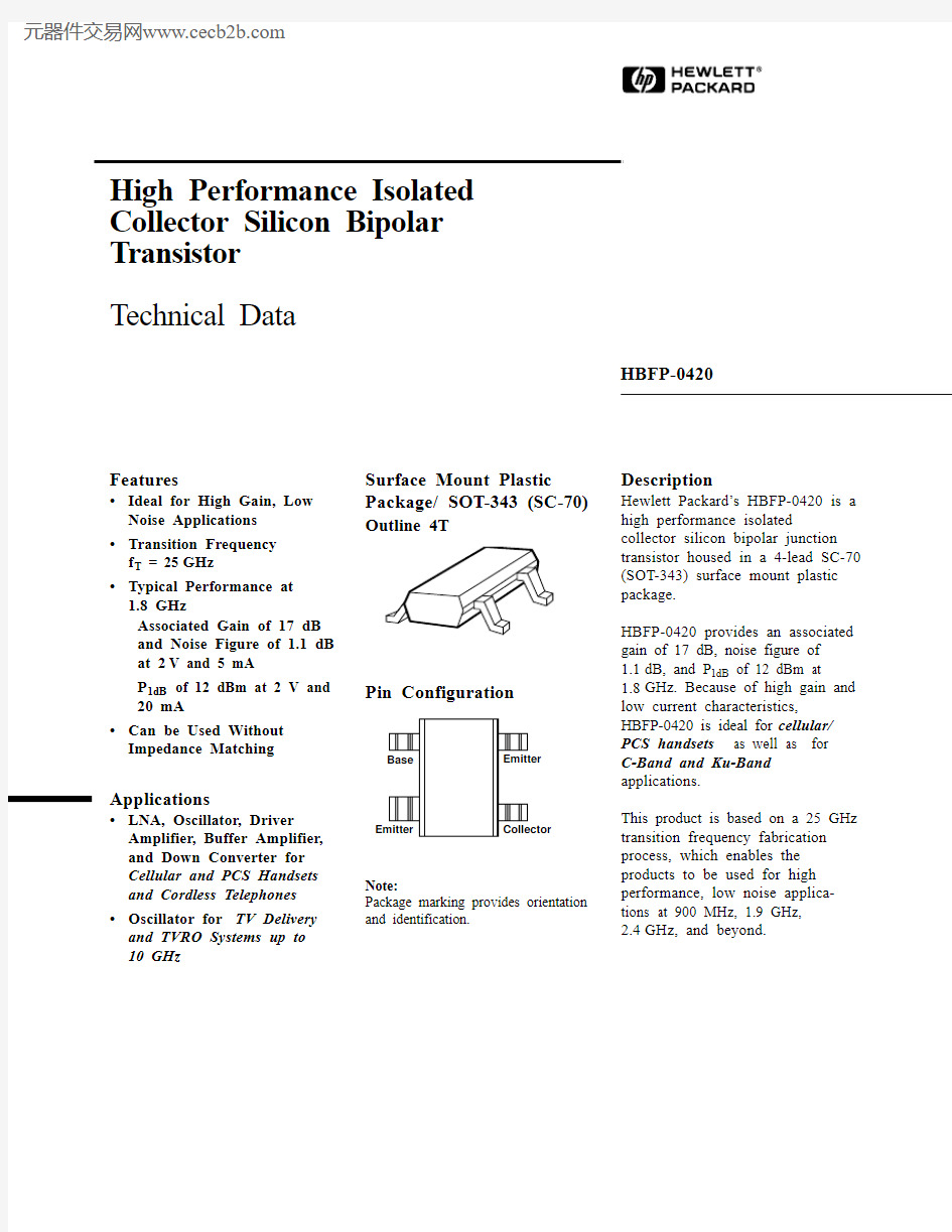
Surface Mount Plastic
Package/SOT-343 (SC-70)
Outline 4T
Pin Configuration
Note:
Package marking provides orientation
and identification.
HBFP-0420 Absolute Maximum Ratings
Absolute Symbol Parameter Units Maximum[1] V
EBO
Emitter-Base Voltage V 1.5
V
CBO
Collector-Base Voltage V15.0
V
CEO
Collector-Emitter Voltage V 4.5
I
C
Collector Current mA36
P
T
Power Dissipation[2]mW162
T
j
Junction Temperature°C150
T
STG Storage Temperature°C-65 to 150
Thermal Resistance:
θjc = 300°C/W
Notes:
1.Permanent damage may occur if
any of these limits are exceeded.
2.P T limited by maximum ratings.
Electrical Specifications, T C = 25°C
Symbol Parameters and Test Conditions Units Min.Typ. Max. DC Characteristics
BV CEO Collector-Emitter Breakdown Voltage I C = 1 mA, open base V 4.5
I CBO Collector-Cutoff Current V CB = 5 V, I E = 0nA150
I EBO Emitter-Base Cutoff Current V EB = 1.5 V, I C = 0μA15
h FE DC Current Gain V CE = 2 V, I C = 5 mA—5080150 RF Characteristics
F MIN Minimum Noise Figure I C = 5 mA, V CE = 2 V, f = 1.8 GHz dB 1.1 1.4
G a Associated Gain I C = 5 mA, V CE = 2 V, f = 1.8 GHz dB15.517
|S21|2Insertion Power Gain I C = 20 mA, V CE = 2 V, f = 1.8 GHz dB17
P-1dB Power Output @ 1 dB I C = 20 mA, V CE = 2 V, f = 1.8 GHz dBm12 Compression Point
HBFP-0420 Typical Scattering Parameters,
V CE = 2 V, I C = 5 mA, T C = 25°C
Freq.S 11
S 21S 12S 22
GHz
Mag
Ang
dB
Mag
Ang
dB
Mag
Ang
Mag
Ang
0.10.746-11.923.414.853171.0-41.40.00984.80.985-6.60.50.682-55.621.912.473139.8-28.50.03863.60.861-29.40.90.607-90.119.99.909116.8-25.00.05649.30.696-46.61.00.585-97.519.39.181112.2-24.50.05946.90.661-49.31.50.532-128.316.8 6.91893.1-22.90.07237.20.516-62.21.80.512-143.115.5 5.95283.4-22.30.07733.20.450-67.72.00.502-151.614.7 5.45378.4-21.90.08031.20.419-71.62.50.490-169.812.9 4.42265.8-21.20.08826.90.359-78.43.00.483-174.611.6 3.78655.2-20.50.09523.40.314-86.33.50.480161.410.3 3.28645.2-19.80.10219.80.286-92.54.00.479149.29.3 2.90835.7-19.20.11016.30.266-98.14.50.482137.68.4 2.62926.5-18.50.11812.50.248-104.15.00.487126.57.6 2.38917.4-17.90.1278.10.233-110.55.50.497115.4 6.9 2.2058.3-17.30.136 3.50.209-117.96.00.513105.0 6.2 2.040-0.8-16.80.145-1.50.189-126.46.50.53294.6 5.6 1.902-9.8-16.30.153-7.10.161-137.17.00.55384.0 5.0 1.778-18.7-15.80.162-12.60.134-152.07.50.57574.5 4.4 1.662-27.5-15.30.171-18.20.115-171.28.00.59266.0 3.9 1.559-36.1-14.90.179-24.00.110167.18.50.60958.2 3.3 1.469-44.4-14.60.186-29.80.113147.29.00.62350.7 2.9 1.393-52.6-14.20.195-35.40.120130.69.50.63543.0 2.4 1.312-60.8-13.90.202-41.60.127118.010.00.64834.5 1.9 1.248-69.1-13.60.209-48.00.130103.9
HBFP-0420 Noise Parameters: V CE = 2 V, I C = 5 mA
Freq.F min Γopt
R N /50
G a GHz dB Mag Ang ?
dB 0.9 1.000.28128.89.622.191.0 1.020.26636.69.221.391.5 1.100.18768.37.618.301.8 1.140.17594.1 6.816.922.0 1.180.154118.4 6.116.212.5 1.250.184146.5 5.414.343.0 1.320.226165.9 5.013.003.5 1.390.254-176.8 4.911.794.0 1.490.292-162.3 5.010.794.5 1.580.312-147.3 6.09.955.0 1.630.355-135.5 6.89.225.5 1.750.375-121.09.38.556.0 1.880.416-108.512.37.996.5 1.940.453-98.115.87.477.0 2.050.486-84.421.4 6.997.5 2.150.506-74.826.8 6.498.0 2.230.532-65.033.6 6.048.5 2.470.556-56.841.7 5.659.0 2.590.589-48.450.4 5.329.5 2.630.610-40.458.2 4.9110.0
2.74
0.624
-31.0
68.3
4.56
S and noise parameters are measured on a microstrip line made on
0.025inch thick alumina carrier. The input reference plane is at the end of the base lead, the output reference plane is at the end of the collector lead. S and noise parameters include the effect of four plated through via holes connecting emitter landing pads on the top of test carrier to the microstrip ground plane on the bottom side of the carrier. Two 0.020inch diameter via holes are placed within 0.010 inch from each emitter lead contact point, one via on each side of that point.
HBFP-0420 Typical Scattering Parameters,
V CE = 2 V, I C = 15 mA, T C = 25°C
Freq.S 11
S 21S 12S 22
GHz
Mag
Ang
dB
Mag
Ang
dB
Mag
Ang
Mag
Ang
0.10.481-22.129.128.438166.1-43.00.00782.30.959-10.50.50.437-91.426.019.969124.7-31.20.02760.70.702-41.40.90.416-131.022.613.526101.9-28.20.03953.40.500-57.21.00.414-138.021.912.37897.8-27.70.04152.90.465-59.61.50.415-163.418.78.61981.9-25.50.05349.60.341-69.81.80.418-174.617.27.25474.2-24.40.06047.90.292-74.42.00.421178.916.3 6.54969.7-23.70.06546.60.269-77.62.50.428165.414.4 5.26259.3-22.30.07742.90.226-84.13.00.435153.612.9 4.41849.9-21.00.08938.80.196-91.13.50.439143.211.6 3.81141.0-19.90.10134.10.177-96.84.00.442133.310.5 3.36232.4-18.90.11329.00.163-102.14.50.447123.79.6 3.02423.9-18.10.12523.70.152-107.25.00.455114.18.8 2.74915.4-17.30.13717.90.138-113.45.50.467104.68.0 2.522 6.8-16.60.14811.80.120-121.16.00.48495.57.3 2.327-1.8-16.00.159 5.40.100-131.46.50.50486.0 6.7 2.163-10.4-15.40.169-1.00.077-148.27.00.52776.7 6.1 2.014-18.9-14.90.179-7.60.059-178.27.50.55268.0 5.5 1.880-27.4-14.50.188-14.30.060144.18.00.57260.4 4.9 1.765-35.5-14.10.197-20.60.077116.68.50.59053.3 4.4 1.658-43.6-13.80.205-27.10.096100.79.00.60446.4 3.9 1.565-51.6-13.40.213-33.60.11289.09.50.61639.2 3.4 1.484-59.6-13.10.221-40.30.12377.910.00.63031.4 3.0 1.406-67.7-12.90.228-47.20.13466.5
HBFP-0420 Noise Parameters: V CE = 2 V, I C = 15 mA
Freq.F min Γopt
R N /50
G a GHz dB Mag Ang ?
dB 0.9 1.570.033-135.58.023.881.0 1.580.054-151.87.823.041.5 1.630.169-155.2 6.719.791.8 1.670.252-148.1 6.318.342.0 1.740.234-158.3 6.417.522.5 1.720.306-149.2 6.115.713.0 1.760.343-142.2 6.514.243.5 1.840.365-133.57.712.974.0 1.890.383-124.49.411.894.5 1.970.407-115.611.511.015.0 2.030.431-106.314.110.225.5 2.150.463-96.817.89.536.0 2.280.483-87.322.98.896.5 2.360.513-77.328.78.327.0 2.420.538-67.835.57.797.5 2.540.560-59.243.07.308.0 2.650.581-51.451.7 6.858.5 2.830.602-44.661.3 6.429.0 2.960.621-37.271.0 5.999.5 3.100.640-29.981.1 5.6110.0
3.14
0.653
-21.8
90.5
5.23
S and noise parameters are measured on a microstrip line made on
0.025inch thick alumina carrier. The input reference plane is at the end of the base lead, the output reference plane is at the end of the collector lead. S and noise parameters include the effect of four plated through via holes connecting emitter landing pads on the top of test carrier to the microstrip ground plane on the bottom side of the carrier. Two 0.020inch diameter via holes are placed within 0.010 inch from each emitter lead contact point, one via on each side of that point.
HBFP-0420 Typical Performance
A S S O C I A T E D G A I N (d
B )
FREQUENCY (GHz)Figure 1. Associated Gain vs.
Frequency and Collector Current at 2 V.
A S S O
C I A T E
D G A I N (d B )
COLLECTOR CURRENT (mA)
Figure 2. Noise Figure vs.
Frequency and Collector Current at 2 V.
Figure 3. Associated Gain vs. Collector Current and Frequency at 2 V.
Figure 5. Associated Gain vs. Voltage (V CE ) at 5 mA.Figure 6. Noise Figure vs. Voltage (V CE ) at 5 mA.
Figure 4. Noise Figure vs. Collector Current and Frequency at 2 V.
N O I S E F I G U R E (d B )
COLLECTOR CURRENT (mA)
VOLTAGE (V)
VOLTAGE (V)
N O I S E F I G U R E (d B )
FREQUENCY (GHz)A S S O C I A T E D G A I N (d B )
N O I S E F I G U R E (d B )
HBFP-0420 Die Model and PSPICE Parameters
AREA= REGION= MODEL=DCS TEMP=
B
E
C IS=I.40507E-17 BV= IBV= IMAX= XTI=
TNOM=21 KF= AF=
ISR= NR= IKF= NBV= IBVL= NBVL= FFE=
RS=
CJO=2.393E-14 TT= EG=
VJ=0.729 M=0.44 N=1 FC=0.8
CMP10
DIODEMODELFORM
# DIODE MODEL #
MODEL = DBC
IS=IE-24 BV= IBV= IMAX= XTI=
TNOM=21 KF= AF=ISR= NR= IKF= NBV= IBVL= NBVL= FFE=
RS=2.17347E2 CJO=8.974E-14 TT= EG= VJ=0.6 M=0.42 N= FC=0.8
CMP12
DIODEMODELFORM
# DIODE MODEL #
MODEL = DCS
IS=IE-24 BV= IBV= IMAX= XTI=
TNOM=21 KF= AF=ISR= NR= IKF= NBV= IBVL= NBVL= FFE=
RS=
CJO=2.593E-14 TT= EG=
VJ=0.8971 M=2.292E-1 N=1.0029 FC=0.8
CMP11
DIODEMODELFORM
# DIODE MODEL #
MODEL = DCE
NPN=yes PNP=
VTF=0.8
ITF=2.21805486E-1 PTF=22 XTB=0.7
APPROXOB=yes
Forward BF=1E6 IKE=1.4737E-1 ISE=7.094E-20 NE=1.006 VAF=4.4E1 NF=1 TF=5.3706E-12 XTF=20Reverse BR=1
IKR=1.1E-2 ISC= NC=2 VAR=3.37 NR=1.005 TR=4E-9Noise KF=
AF= KB= AB=
FB=Diode and junction EG=1.17 IS=4.4746E-18
IMAX= XTI=3 TNOM=21 Substrate IS5= NS=Parasitics RB=9.30144818 IRB=3.029562E-6 RBM=.1 RE= RC= CJC=2.7056E-14 VJC=.6775 MJC=0.3319 FC=0.8 CJE=7.474248E-14 VJE=0.9907
MJE=0.5063 CJS=
VJS= MJS=
CMP68 BITMODELFORM
# BJT MODEL #
MODEL = BJTMODEL
XCJC=4.39790997E-1This model can be used as a design tool. It has been tested on MDS for various specifications. However, for more precise and accurate design, please refer to the measured data in this data sheet.
Note:The value of beta was high (BF =1E6) to compensate for the fact that diode DBE reduces the current going into the
base (current flows through DBE). The diodes are necessary to model the non-linear effects.
SOT343 Package Model
Package Dimensions
SOT-343 (SC-70 4 Lead)
Part Number Ordering Information
Part Number Devices per Reel
Container HBFP-0420-TR130007" Reel HBFP-0420-TR210,00013" Reel HBFP-0420-BLK
100
antistatic bag
b TYP
θ
DIMENSIONS ARE IN MILLIMETERS (INCHES)
DIMENSIONS
MIN.
0.80 (0.031)
0 (0)
0.25 (0.010)
0.10 (0.004)
1.90 (0.075)
2.00 (0.079)
0.55 (0.022)
0.450 TYP (0.018)
1.15 (0.045)
0.10 (0.004)
MAX. 1.00 (0.039) 0.10 (0.004) 0.35 (0.014) 0.20 (0.008) 2.10 (0.083) 2.20 (0.087) 0.65 (0.025) 1.35 (0.053) 0.35 (0.014) 10SYMBOL
A A1 b C D E e h E1 L θ
Device Orientation
Tape Dimensions
For Outline 4T
USER FEED
END VIEW
TOP VIEW (CARRIER TAPE THICKNESS)
DESCRIPTION
SYMBOL SIZE (mm)SIZE (INCHES)LENGTH WIDTH DEPTH PITCH
BOTTOM HOLE DIAMETER A 0B 0K 0P D 1 2.24 ± 0.102.34 ± 0.101.22 ± 0.104.00 ± 0.101.00 + 0.250.088 ± 0.0040.092 ± 0.0040.048 ± 0.0040.157 ± 0.0040.039 + 0.010CAVITY
DIAMETER PITCH POSITION D P 0E 1.55 ± 0.054.00 ± 0.101.75 ± 0.100.061 ± 0.0020.157 ± 0.0040.069 ± 0.004PERFORATION
WIDTH
THICKNESS
W t 18.00 ± 0.300.255 ± 0.0130.315 ± 0.0120.010 ± 0.0005CARRIER TAPE CAVITY TO PERFORATION (WIDTH DIRECTION)CAVITY TO PERFORATION (LENGTH DIRECTION)
F P 2
3.50 ± 0.052.00 ± 0.05
0.138 ± 0.0020.079 ± 0.002
DISTANCE
https://www.doczj.com/doc/f212805174.html,/go/rf
For technical assistance or the location of your nearest Hewlett-Packard sales office, distributor or representative call: Americas/Canada: 1-800-235-0312 or
408-654-8675
Far East/Australasia: Call your local HP sales office.
Japan: (81 3) 3335-8152
Europe: Call your local HP sales office. Data subject to change.
Copyright ? 1998 Hewlett-Packard Co. Printed in U.S.A. 5968-0129E (6/98)