Data Sheet No. PD60172 Rev.G
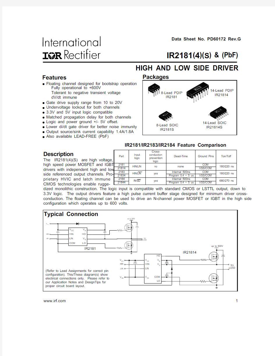
Features
?Fully operational to +600V
dV/dt immune
????????
IR2181(4)(S ) & (PbF)
https://www.doczj.com/doc/fb9682430.html, 1
Description
dized monolithic construction. The logic input is compatible with standard CMOS or LSTTL output, down to 3.3V logic. The output drivers feature a high pulse current buffer stage designed for minimum driver cross-conduction. The floating channel can be used to drive an N-channel power MOSFET or IGBT in the high side configuration which operates up to 600 volts.
IR2181(4) (S
) & (PbF)
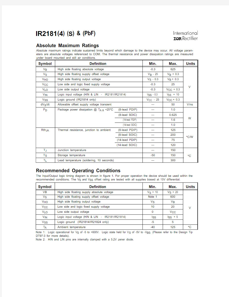
Absolute Maximum Ratings
Absolute maximum ratings indicate sustained limits beyond which damage to the device may occur. All voltage param-eters are absolute voltages referenced to COM. The thermal resistance and power dissipation ratings are measured Note 1: Logic operational for V S of -5 to +600V. Logic state held for V S of -5V to -V BS . (Please refer to the Design Tip DT97-3 for more details).
Note 2: HIN and LIN pins are internally clamped with a 5.2V zener diode.
Recommended Operating Conditions
The Input/Output logic timing diagram is shown in figure 1. For proper operation the device should be used within the recommended conditions. The V and V offset rating are tested with all supplies biased at 15V differential.
) & (PbF)
IR2181(4) (S
IR2181(4) (S
) & (PbF) Functional Block Diagrams
IR2181(4) (S
) & (PbF)
Lead Assignments
8-Lead PDIP 8-Lead SOIC
Lead Definitions
Symbol Description
HIN Logic input for high side gate driver output (HO), in phase (IR2181/IR21814)LIN Logic input for low side gate driver output (LO), in phase (IR2181/IR21814)VSS Logic Ground (IR21814 only)V B High side floating supply HO High side gate drive output V S High side floating supply return V CC Low side and logic fixed supply LO Low side gate drive output COM
Low side return
IR2181IR2181S
1234
8
765
HIN LIN COM LO
V B HO V S V CC
1234
8
765
HIN LIN COM LO
V B HO V S V CC
1234567
14
1312111098
HIN LIN VSS
COM LO V CC
V B HO V S
1234567
14
1312111098
HIN LIN VSS
COM LO V CC
V B HO V S
14-Lead PDIP
14-Lead SOIC
IR21814IR21814S
IR2181(4) (S
) & (PbF)
HIN
LIN
HO
LO
Figure 2. Switching Time Waveform Definitions
Figure 3. Delay Matching Waveform Definitions
IR2181(4) (S
) & (PbF)
IR2181(4) (S
) & (PbF)
) & (PbF)
IR2181(4) (S
IR2181(4) (S
) & (PbF)
IR2181(4) (S
) & (PbF)
IR2181(4) (S
) & (PbF)
) & (PbF)
IR2181(4) (S
IR2181(4) (S
) & (PbF)
IR2181(4) (S
) & (PbF)
IR2181(4) (S
) & (PbF)
,
IR2181(4) (S
) & (PbF)
,
IR2181(4) (S
) & (PbF)
,
Case outlines