
General Description
The MAX9660 evaluation kit (EV kit) demonstrates the MAX9660 programmable VCOM voltage buffer used for VCOM backplane voltage calibration in TFT-LCD pan-els, such as those found in high-resolution TVs, and high-end monitors. A 7-bit digital-to-analog converter (DAC) sinks current from an external resistor-divider to set a VCOM reference voltage. An external resistor sets the full-scale range of sinking current. The IC can drive ±100mA continuous current and up to ±900mA peak current. The desired DAC value can be stored in non-volatile multiple one-time programmable (MOTP) mem-ory and is recalled at each power-up. The EV kit oper-ates from an 8V to 20V DC power supply.
The MAX9660 EV kit features a USB-to-I 2C interface cir-cuit. Windows ?2000/XP ?- and Windows Vista ?-com-patible software, with a graphical user interface (GUI),available for exercising the MAX9660 features. The EV kit can also connect to a user-supplied I 2C interface circuit for stand-alone MAX9660 operation.
Features
o 7-Bit DAC for Setting VCOM Reference Voltage o Integrated 30x Programmable Nonvolatile MOTP Memory to Store VCOM Setting o ±100mA Continuous Current o ±900mA Peak Current
o 8V to 20V DC Power-Supply Operation o USB-Powered USB-to-I 2C Interface Circuit o Windows 2000/XP- and Windows Vista (32-Bit)-Compatible Software o Lead(Pb)-Free and RoHS Compliant o Proven PCB Layout
o Fully Assembled and Tested
Evaluates: MAX9660
MAX9660 Evaluation Kit
________________________________________________________________Maxim Integrated Products 1
19-4528; Rev 0; 3/09
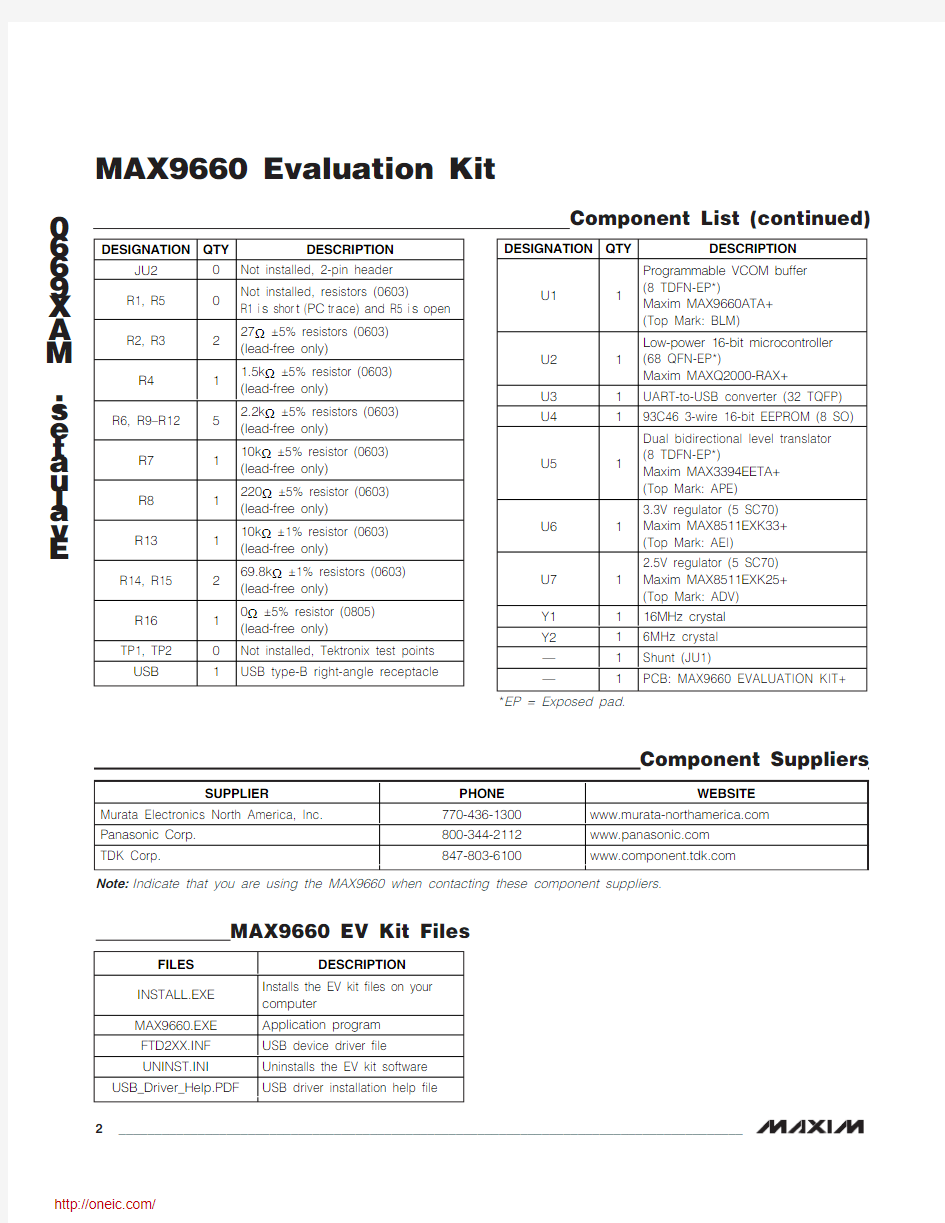
Component List
For pricing, delivery, and ordering information, please contact Maxim Direct at 1-888-629-4642,or visit Maxim’s website at https://www.doczj.com/doc/f49603729.html,.
Ordering Information
+Denotes lead(Pb)-free and RoHS compliant.
Windows, Windows XP, and Windows Vista are registered trademarks of Microsoft Corp.
E v a l u a t e s : M A X 9660
MAX9660 Evaluation Kit 2_______________________________________________________________________________________
Component List (continued)
Quick Start
Required Equipment ?MAX9660 EV kit (USB cable included)
?User-supplied Windows 2000/XP or Windows Vista PC with a spare USB port
?8V to 20V DC power supply at 1A
?One digital voltmeter (DVM)
Note: In the following sections, software-related items are identified by bolding. Text in bold refers to items directly from the EV kit software. Text in bold and under-lined refers to items from the Windows operating system.
Procedure The MAX9660 EV kit is fully assembled and tested. Follow the steps below to verify board operation:
1)Visit https://www.doczj.com/doc/f49603729.html,/evkitsoftware to down-
load the latest version of the EV kit software, 9660Rxx.ZIP. Save the EV kit software to a tempo-rary folder and uncompress the ZIP file.
2)Install the EV kit software on your computer by run-
ning the INSTALL.EXE program inside the tempo-rary folder. The program files are copied and icons are created in the Windows Start | Programs menu.
3)Connect the USB cable from the PC to the EV kit
board. A N ew Hardware Found window pops up when installing the USB driver for the first time. If a window is not seen that is similar to the one described above after 30s, remove the USB cable from the board and reconnect it. Administrator priv-ileges are required to install the USB device driver on Windows.
4)Follow the directions of the Add N ew Hardware
Wizard to install the USB device driver. Choose the Search for the best driver for your device option.
Specify the location of the device driver to be C:\Program Files\MAX9660(default installation directory) using the Browse button. During device driver installation, Windows may show a warning message indicating that the device driver Maxim uses does not contain a digital signature. This is not an error condition and it is safe to proceed with instal-lation. Refer to the USB_Driver_Help.PDF document included with the software for additional information.
5)Once the software and hardware installation is com-
plete, disconnect the USB cable from the EV kit.
6)Verify that a shunt is installed on jumper JU1 pins
2-3 (on-board 3.3V digital power supply).
7)Set the power supply to 15V and disable the
power-supply output.
8)Connect the power-supply positive terminal to the
AVDD PCB pad and the negative terminal to the
GND PCB pad next to AVDD.
9)Connect the DVM negative terminal to the GND
PCB pad next to the VCOMOUT PCB pad.
10)Connect the DVM positive terminal to the VCOMOUT
PCB pad.
11)Connect the USB cable to the EV kit.
12)Enable the power-supply output.
13)Start the MAX9660 EV kit software by opening its
icon in the Start | Programs menu. The EV kit soft-
ware main window appears, as shown in Figure 1.
14)Use the DVM to verify that the output voltage is close
to the voltage shown in the Output (V) edit box.
15)To power down the EV kit, first turn off the AVDD
supply and then disconnect the USB cable.
Detailed Description of Software The MAX9660 EV kit GUI software provides a user inter-
face (Figure 1) to control the features of the MAX9660
VCOM voltage buffer. To start the EV kit software, dou-
ble-click the MAX9660 EV kit icon created during instal-
lation. The software has a demo mode that is available
by selecting Options | Demo Mode from the menu bar.
When in demo mode, all software communication to the
EV kit hardware is disabled and most of the software’s
GUI is functional. This feature enables a user to evalu-
ate the software without hardware connectivity.
The user interface is easy to operate; use the mouse, or
press the Tab and arrow keys to navigate the window.
Press the Enter key after modifying an edit box to
update the software. The status bar located at the bot-
tom-left of the GUI window displays EV kit connectivity
status, while the lower-right status bar displays the
device address.
The VCOM output voltage in the Output (V)edit box is
calculated using the values in the Reference group
box’s AVDD (V), R13 (kOhm), R14 (kOhm), and R15
(kOhm)edit boxes. The edit-box values in the
Reference group box MUST be correct for the soft-
ware’s VCOM output voltage calculation to be correct.
Evaluates: MAX9660 MAX9660 Evaluation Kit
_______________________________________________________________________________________3
E v a l u a t e s : M A X 9660
Upon startup, the DAC is set to the last value stored in the MOTP register. To modify the DAC output or the MOTP register setting, click on the DAC or MOTP radio button, respectively, in the Register group box and perform one of the following in the VCOM group box:1)Move the scrollbar, or
2)Type a register value directly into the Reg Value
edit box (7-bit decimal equivalent), or 3)Type in the desired output voltage in the Output (V)
edit box. The software uses a register value that generates a voltage closest to the desired voltage value.Press the Write button to update the MAX9660 IC with the entered register value. Data written to the DAC is volatile. Data can be written 30x to the nonvolatile MOTP register. The factory-default MOTP register set-ting is 64.
The Options menu item provides access to an advanced 2-wire interface and demo mode. The Help menu item provides help and general information about the EV kit software. The File menu item provides the option to exit the EV kit software.
VCOM Voltage Calculation
The VCOM voltage is calculated using an on-board resistor-divider (R14 and R15), a resistor (R13) that sets the full-scale sink current, AVDD voltage, and the deci-mal DAC code (CODE) as follows:
where CODE ranges from 0 to 127.
The VCOM voltage can be measured across the VCOMOUT and GND PCB pads.
Advanced User Interface
A serial interface can be used by advanced users by selecting Options | Interface (Advanced Users)from the menu bar.
Click on the 2-wire interface tab shown in Figure 2.Press the Hunt for active listeners button and select the MAX9660 slave address 0x9E from the Target Device Address:combo box. In the General commands tab sheet, select the S - SMBusSendByte(addr,cmd)item in the drop-down list. Enter the desired hexadecimal data values into the Command byte:combo box and press the Execute
button.
MAX9660 Evaluation Kit 4
_______________________________________________________________________________________
Figure 1. MAX9660 Evaluation Software Main Window
Detailed Description of Hardware
The MAX9660 evaluation kit (EV kit) demonstrates the MAX9660 programmable VCOM voltage buffer in an 8-pin TDFN surface-mount package with an exposed pad. EV kit applications include e-paper display pan-els, VCOM backplane voltage calibration in TFT-LCD panels, such as those found in high-resolution TVs and high-end monitors. A 7-bit digital-to-analog converter (DAC) sinks current from an external resistor-divider (R14 and R15) to set a VCOM reference voltage. An external resistor (R13) sets the full-scale range of sink-
ing current. The IC can drive ±100mA continuous cur-rent and up to ±900mA peak current. The desired DAC value can be stored in nonvolatile MOTP memory and is recalled at each power-up. The EV kit operates from an 8V to 20V DC power supply that supplies up to 1A.The MAX9660 EV kit features a USB-to-I 2C interface cir-cuit using Maxim’s MAXQ2000 microcontroller and MAX3394E level translator. The interface circuit pro-vides 3.3V to the digital DVDD input from the USB power. The EV kit can also connect to a user-supplied I 2C interface circuit for stand-alone MAX9660 operation.
Evaluates: MAX9660
MAX9660 Evaluation Kit
_______________________________________________________________________________________
5
Figure 2. Advanced I 2C User Interface Window (2-Wire Interface Tab)
E v a l u a t e s : M A X 9660
Digital Supply Configuration
The MAX9660 EV kit provides two options to power the MAX9660 digital supply DVDD. DVDD can operate from the 3.3V supply generated by the USB-to-I 2C interface circuit or from a user-supplied 2.5V to 3.6V DC power supply connected across the DIN and DGND PCB pads. See Table 1 to configure DVDD using jumper JU1.
Stand-Alone User-Supplied I 2C
Communication
The MAX9660 EV kit can be used in stand-alone opera-tion to interface with a user’s I 2C system without using a PC. In stand-alone operation, I 2C communication oper-ates from 2.5V to 3.6V. To use the MAX9660 EV kit with a user-supplied I 2C interface, perform the following steps:
1)Disconnect the USB cable from the EV kit.
2)Cut open header J1 shorting traces on the PCB
bottom layer.3)Move jumper JU1 shunt to pins 1-2 (user-supplied
digital power supply).4)Connect the positive terminal of a user-supplied
2.5V to
3.6V DC power supply to the DIN PCB pad and the negative terminal to the nearby DGND PCB pad.5)Remove SDA and SCL pullup resistors R11 and
R12 if not needed.6)Connect the user-supplied I 2C interface signals to
the EV kit PCB pads, as shown in Table 2.
MAX9660 Evaluation Kit 6_______________________________________________________________________________________
***Disconnect the USB cable from the EV kit.
Evaluates: MAX9660
MAX9660 Evaluation Kit
_______________________________________________________________________________________
7
Figure 3. MAX9660 EV Kit Schematic—VCOM Buffer Circuit
E v a l u a t e s : M A X 9660
MAX9660 Evaluation Kit 8
_______________________________________________________________________________________
Figure 4. MAX9660 EV Kit Schematic—USB-to-I C Circuit
Evaluates: MAX9660
MAX9660 Evaluation Kit
_______________________________________________________________________________________
9
Figure 5. MAX9660 EV Kit Component Placement Guide—Component Side
E v a l u a t e s : M A X 9660
MAX9660 Evaluation Kit 10
______________________________________________________________________________________
Figure 6. MAX9660 EV Kit PCB Layout—Component Side
分销商库存信息: MAXIM
MAX9660EVKIT+