General Description
Maxim’s MAX312L/MAX313L/MAX314L analog switch-es feature low on-resistance (10?max) and 1.5?on-resistance matching between channels. These switches are +3V logic compatible when powered from ±15V or +12V supplies. The switches conduct equally well in either direction, and offer low leakage over temperature (2.5nA at +85°C).
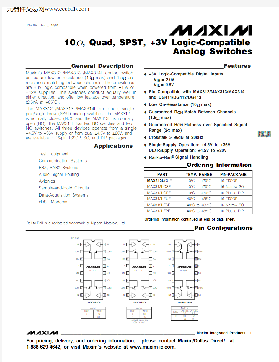
The MAX312L/MAX313L/MAX314L are quad, single-pole/single-throw (SPST) analog switches. The MAX312L is normally closed (NC), and the MAX313L is normally open (NO). The MAX314L has two NC switches and two NO switches. All three devices operate from a single +4.5V to +36V supply or from dual ±4.5V to ±20V, and are available in 16-pin TSSOP, SO, and DIP packages.
Applications
Test Equipment Communication Systems PBX, PABX Systems Audio Signal Routing Avionics
Sample-and-Hold Circuits Data-Acquisition Systems xDSL Modems
Features
o +3V Logic-Compatible Digital Inputs
V IH = 2.0V V IL = 0.8V
o Pin Compatible with MAX312/MAX313/MAX314and DG411/DG412/DG413o Low On-Resistance (10?max)
o Guaranteed R ON Match Between Channels (1.5?max)o Guaranteed R ON Flatness over Specified Signal Range (2?max)o Crosstalk > 96dB at 20kHz
o Single-Supply Operation: +4.5V to +36V Dual-Supply Operation: ±4.5V to ±20V o Rail-to-Rail ?Signal Handling
MAX312L/MAX313L/MAX314L
10?, Quad, SPST, +3V Logic-Compatible
Analog Switches
________________________________________________________________Maxim Integrated Products 1
Ordering Information
19-2184; Rev 0; 10/01
For pricing, delivery, and ordering information,please contact Maxim/Dallas Direct!at 1-888-629-4642, or visit Maxim’s website at https://www.doczj.com/doc/f08298365.html,.
Rail-to-Rail is a registered trademark of Nippon Motorola, Ltd.
Ordering Information continued at end of data sheet.
Pin Configurations
M A X 312L /M A X 313L /M A X 314L
10?, Quad, SPST, +3V Logic-Compatible Analog Switches 2_______________________________________________________________________________________
ABSOLUTE MAXIMUM RATINGS
ELECTRICAL CHARACTERISTICS —Dual Supplies
(V+ = +15V, V- = -15V, GND = 0, V IH = 2.0V, V IL = 0.8V, T A = T MIN to T MAX , unless otherwise noted. Typical values are at T A =
Stresses beyond those listed under “Absolute Maximum Ratings” may cause permanent damage to the device. These are stress ratings only, and functional operation of the device at these or any other conditions beyond those indicated in the operational sections of the specifications is not implied. Exposure to absolute maximum rating conditions for extended periods may affect device reliability.
(Voltages Referenced to GND)
V+...........................................................................-0.3V to +44V V-............................................................................+0.3V to -44V V+ to V-...................................................................-0.3V to +44V V IN_to V-................................................................-0.3V to +44V All Other Pins (Note 1)..........................(V- - 0.3V) to (V+ + 0.3V)Continuous Current (COM_, NO_, NC_) ........................±100mA Peak Current (COM_, NO_, NC_)
(pulsed at 1ms, 10% duty cycle max)........................±300mA
Continuous Power Dissipation (T A = +70°C)
TSSOP (derate 6.7mW/°C above +70°C)...................457mW Narrow SO (derate 8.70mW/°C above +70°C)...........696mW Plastic DIP (derate 10.53mW/°C above +70°C).........842mW Operating Temperature Ranges
MAX31_LC_E.....................................................0°C to +70°C MAX31_LE_E..................................................-40°C to +85°C Storage Temperature Range ............................-65°C to +150°C Junction Temperature......................................................+150°C Lead Temperature (soldering, 10s).................................+300°C
Note 1:Signals on COM_, NO_, or NC_ exceeding V+ or V- are clamped by internal diodes. Limit forward-diode current to maxi-mum current rating.
MAX312L/MAX313L/MAX314L
10?, Quad, SPST, +3V Logic-Compatible
Analog Switches
ELECTRICAL CHARACTERISTICS —Dual Supplies (continued)
(V+ = +15V, V- = -15V, GND = 0, V = 2.0V, V = 0.8V, T = T to T , unless otherwise noted. Typical values are at T =ELECTRICAL CHARACTERISTICS —Single Supply
(V+ = +12V, V- = 0, GND = 0, V IH = 2.0V, V IL = 0.8V, T A = T MIN to T MAX , unless otherwise noted. Typical values are at T A = +25°C.)
M A X 312L /M A X 313L /M A X 314L
10?, Quad, SPST, +3V Logic-Compatible Analog Switches 4_______________________________________________________________________________________
ELECTRICAL CHARACTERISTICS —Single Supply (continued)
(V+ = +12V, V- = 0, GND = 0, V
= 2.0V, V = 0.8V, T = T to T , unless otherwise noted. Typical values are at T = +25°C.) Note 4:?R ON = ?R ON max - ?R ON min.
Note 5:Flatness is defined as the difference between the maximum and minimum value of on-resistance as measured over the
specified analog signal range.
Note 6:Leakage parameters are 100% tested at maximum-rated hot temperature and guaranteed by correlation at +25°C.Note 7:Guaranteed by design.
Note 8:Off-isolation = 20log 10[V COM /(V NC or V NO )], V COM = output, V NC or V NO = input to off switch.Note 9:Between any two switches.
MAX312L/MAX313L/MAX314L
10?, Quad, SPST, +3V Logic-Compatible
Analog Switches
_______________________________________________________________________________________5
264108141216ON-RESISTANCE vs. V COM
(DUAL SUPPLIES)
V COM (V)
R O N (?)
-20
-10
010
20
40
3020100
105
15
20
ON-RESISTANCE vs. V COM
(SINGLE SUPPLY)
V COM (V)
R O N (?
)
2
3
45
678910
-15
-5
5
15
ON-RESISTANCE vs. V COM AND TEMPERATURE (DUAL SUPPLIES)
V COM (V)R O N (?
)
04
128
16
20
ON-RESISTANCE vs. V COM AND TEMPERATURE (SINGLE SUPPLY)
V COM (V)
R O N (?)
63
9
12
0.0001
0.001
0.1
0.01
110-40
10
-15
35
60
85
OFF- AND ON-LEAKAGE CURRENT
vs. TEMPERATURE
TEMPERATURE (°C)
L E A K A G E C U R R E N T (n A )
-60
-20-402006040
80
-15-50-1051015
CHARGE INJECTION
vs. V COM
V COM (V)
Q (p C )
0.0000001
0.000001
0.0001
0.00001
0.0010.01
-40
10
-15
35
60
85
SUPPLY CURRENT vs.TEMPERATURE
TEMPERATURE (°C)
I +, I -
, I L (μA )
0.1
0.01
0.001
0.0001
10
1k 100
10k
100k
TOTAL HARMONIC DISTORTION
vs. FREQUENCY
FREQUENCY (Hz)
T H D (%
)
-20-40
-60
-80
0.1
10
1
100
1000
FREQUENCY RESPONSE
FREQUENCY (MHz)
L O S S (d B )
Typical Operating Characteristics
(T A = +25°C, unless otherwise noted.)
M A X 312L /M A X 313L /M A X 314L
10?, Quad, SPST, +3V Logic-Compatible Analog Switches 6_______________________________________________________________________________________
-50
-20-30-40-10010203040500
6
3
9
12
15
SUPPLY CURRENT vs. LOGIC INPUT VOLTAGE
LOGIC INPUT VOLTAGE (V)
S U P P L Y C U R R E N T (μA )
85
95
105
115
-15
-5
0-10
5
10
15
TURN-ON/TURN-OFF TIME vs.V COM (DUAL SUPPLIES)
V COM (V)
T U R N -O N /T U R N -O F F T I M E (n s )
180
160
140
120
100
63
9
12
TURN-ON/TURN-OFF TIME vs.V COM (SINGLE SUPPLY)
V COM (V)
T U R N -O N /T U R N -O F F T I M E (n s )
6080
120
100
140
160
-50
-25
25
50
75
100
TURN-ON/TURN-OFF TIME vs. TEMPERATURE
TEMPERATURE (°C)
T U R N -O N /T U R N -O F F T I M E (n s )
0.8
1.21.01.61.41.8
2.0412
81620
LOGIC THRESHOLD vs. SUPPLY VOLTAGE
SUPPLY VOLTAGE (V)
L O G I C T H R E S H O L D (V )
100
300200500400
600700±3±9±6±12±15
TURN-ON/TURN-OFF TIME vs.
SUPPLY VOLTAGE
SUPPLY VOLTAGE (V)
T U R N -O N /T U R N -O F F T I M E (n s )
Typical Operating Characteristics (continued)
(T A = +25°C, unless otherwise noted.)
Applications Information
Low-Distortion Audio The MAX312L/MAX313L/MAX314L, having very low R ON and very low R ON variation with signal amplitude, are well suited for low-distortion audio applications. The Typical Operating Characteristics show Total Harmonic Distortion (THD) vs. Frequency graphs for several signal amplitudes and impedances. Higher source and load impedances improve THD, but reduce off-isolation.
Off-Isolation at High Frequencies In 50?systems, the high-frequency on-response of these parts extends from DC to above 100MHz with a typical loss of -2dB. When the switch is turned off, how-ever, it behaves like a capacitor, and off-isolation decreases with increasing frequency. (Above 300MHz, the switch actually passes more signal turned off than turned on.) This effect is more pronounced with higher source-and-load impedances.
Above 5MHz, circuit board layout becomes critical, and it becomes difficult to characterize the response of the switch independent of the circuit. The graphs shown in the Typical Operating Characteristics were taken using a 50?source and load connected with BNC connectors.
Power-Supply Sequencing-Free
Operation
Most CMOS switches require specific power-supply sequencing in order to prevent the devices from latching
up. The older MAX312/MAX313/MAX314 devices require
a proper power-supply sequence of V+, V L, V-, and so forth. Otherwise, it becomes necessary to add signal diodes to the circuit in order to protect it from potential latchups. The new MAX312L/MAX313L/ MAX314L devices eliminate the need for a V L pin and permit the
user to utilize any power-up sequence that is required. It
is, however, important not to exceed the absolute maxi-
mum ratings because stresses beyond the listed ratings
may cause permanent damage to the devices.
Chip Information TRANSISTOR COUNT: 92
PROCESS: CMOS MAX312L/MAX313L/MAX314L
10?, Quad, SPST, +3V Logic-Compatible
Analog Switches _______________________________________________________________________________________7
M A X 312L /M A X 313L /M A X 314L
10?, Quad, SPST, +3V Logic-Compatible Analog Switches 8_______________________________________________________________________________________
Figure 1. Switching-Time Test Circuit
Figure 2. Break-Before-Make Test Circuit (MAX314L only)
MAX312L/MAX313L/MAX314L
10?, Quad, SPST, +3V Logic-Compatible
Analog Switches
_______________________________________________________________________________________9
Figure 3. Charge Injection Test Circuit
Figure 4. Off-Isolation Test Circuit Figure 5. Crosstalk Test Circuit
M A X 312L /M A X 313L /M A X 314L
10?, Quad, SPST, +3V Logic-Compatible Analog Switches 10______________________________________________________________________________________
Figure 6. Channel Off-Capacitance Test Circuit Figure 7. Channel On-Capacitance Test Circuit
Ordering Information (continued)
MAX312L/MAX313L/MAX314L
10?, Quad, SPST, +3V Logic-Compatible
Analog Switches
______________________________________________________________________________________11
Package Information
M A X 312L /M A X 313L /M A X 314L
10?, Quad, SPST, +3V Logic-Compatible Analog Switches
Package Information (continued)
MAX312L/MAX313L/MAX314L
10?, Quad, SPST, +3V Logic-Compatible
Analog Switches
Maxim cannot assume responsibility for use of any circuitry other than circuitry entirely embodied in a Maxim product. No circuit patent licenses are implied. Maxim reserves the right to change the circuitry and specifications without notice at any time.
Maxim Integrated Products, 120 San Gabriel Drive, Sunnyvale, CA 94086 408-737-7600 ____________________13?2001 Maxim Integrated Products
Printed USA
is a registered trademark of Maxim Integrated Products.
Package Information (continued)