PRELIMINARY DATA SHEET
SKY77824-11 Power Amplifier Module for FDD LTE Bands 7 and 30, TDD LTE Bands 38/41 and 40, and AXGP Band
Applications
?Long-Term Evolution (LTE)?Evolved Universal Terrestrial
Radio Access Networks (EUTRAN)
?Handsets and Data Cards Features
?Optimized for Average Power Tracking (APT)
?High efficiency Broadband
2.3GHz to 2.69 GHz
?MIPI?RFFE interface ?Integrated output switch including TDD Tx/Rx function for single SAW architecture
?RF I/O internally matched to 50 ohms
?Small, low profile package
-4.0x 3.65x 0.8 mm Max.
-28-pad configuration Description
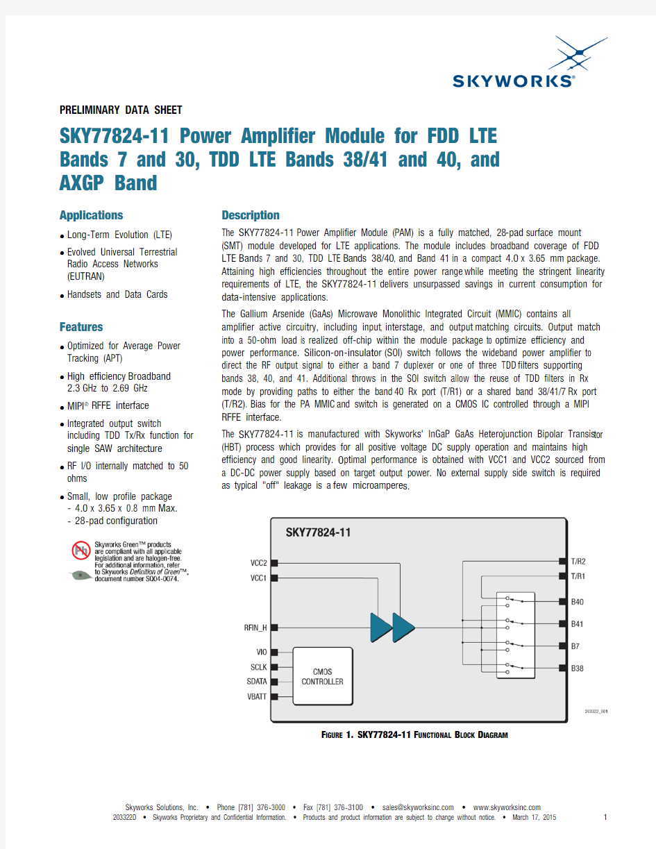
The SKY77824-11Power Amplifier Module (PAM) is a fully matched, 28-pad surface mount (SMT) module developed for LTE applications. The module includes broadband coverage of FDD LTE Band s 7 and 30, TDD LTE Bands 38/40, and Band 41in a compact 4.0x 3.65 mm package. Attaining high efficiencies throughout the entire power range while meeting the stringent linearity requirements of LTE, the SKY77824-11delivers unsurpassed savings in current consumption for data-intensive applications.
The Gallium Arsenide (GaAs) Microwave Monolithic Integrated Circuit (MMIC) contains all amplifier active circuitry, including input, interstage, and output matching circuits. Output match into a 50-ohm load is realized off-chip within the module package to optimize efficiency and power performance. Silicon-on-insulator(S OI) switch follows the wideband power amplifier to direct the RF output signal to either a band 7 duplexer or one of three TDD filters supporting bands 38, 40, and 41. Additional throws in the SOI switch allow the reuse of TDD filters in Rx mode by providing paths to either the band40 Rx port (T/R1) or a shared band 38/41/7Rx port (T/R2). Bias for the PA MMIC and switch is generated on a CMOS IC controlled through a MIPI RFFE interface.
The SKY77824-11is manufactured with Skyworks' InGaP GaAs Heterojunction Bipolar Transis tor (HBT) process which provides for all positive voltage DC supply operation and maintains high efficiency and good linearity. O ptimal performance is obtained with VCC1 and VCC2 sourced from a DC-DC power supply based on target output power. No external supply side switch is required as typical "off" leakage is a few microampere s.
F IGURE 1.SKY77824-11F UNCTIONAL B LOCK D
IAGRAM
PRELIMINARY DATA SHEET SKY77824-11 POWER AMPLIFIER MODULE for
FDD LTE BANDS 7 and 30,TDD LTE BANDS 38/41 and 40, and AXGP BAND
Electrical Specifications
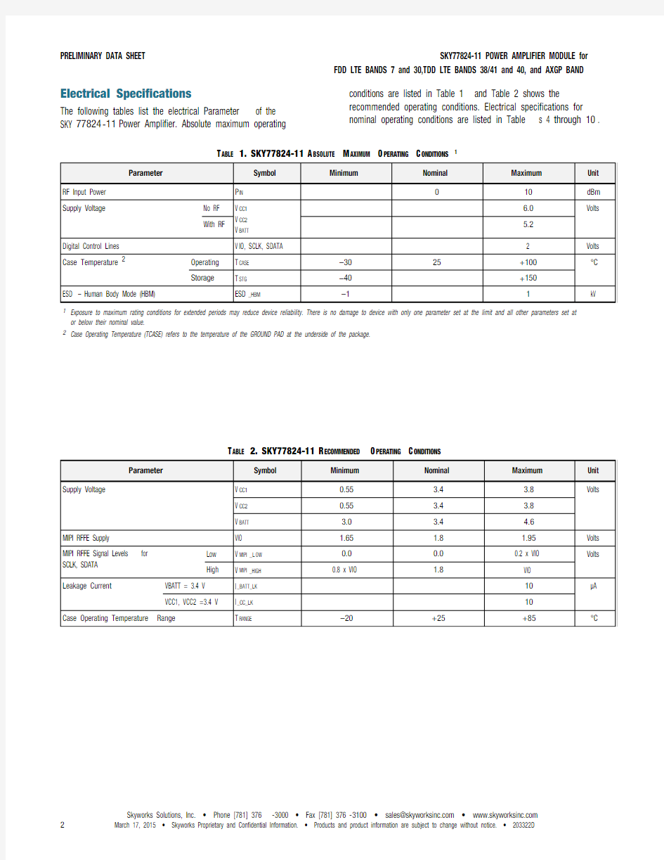
The following tables list the electrical Parameter of the SKY77824-11Power Amplifier. Absolute maximum operating conditions are listed in Table 1and Table 2 shows the recommended operating conditions. Electrical specifications for nominal operating conditions are listed in Table s 4 through 10.
T ABLE 1.SKY77824-11A BSOLUTE M AXIMUM O PERATING C ONDITIONS1
Parameter Symbol Minimum Nominal Maximum Unit RF Input Power P IN010dBm
Supply Voltage No RF V CC1
V CC2
V BATT 6.0Volts
With RF 5.2
Digital Control Lines V IO, SCLK, SDATA 2 Volts Case Temperature2Operating T CASE–3025+100°C
Storage T STG–40+150
ESD – Human Body Mode (HBM)ESD_HBM–11kV
1Exposure to maximum rating conditions for extended periods may reduce device reliability. There is no damage to device with only one parameter set at the limit and all other parameters set at or below their nominal value.
2Case Operating Temperature (TCASE) refers to the temperature of the GROUND PAD at the underside of the package.
T ABLE 2.SKY77824-11R ECOMMENDED O PERATING C ONDITIONS
Parameter Symbol Minimum Nominal Maximum Unit Supply Voltage V CC10.55 3.4 3.8Volts
V CC20.55 3.4 3.8
V BATT 3.0 3.4 4.6
MIPI RFFE Supply VIO 1.65 1.8 1.95Volts
MIPI RFFE Signal Levels for SCLK, SDATA Low V MIPI_L OW0.00.00.2 x VIO Volts High V MIPI_HIGH0.8 x VIO 1.8VIO
Leakage Current VBATT = 3.4 V I_BATT_LK10μA VCC1, VCC2 =3.4 V I_CC_LK10
Case Operating Temperature Range T RANGE–20+25+85°C
SKY77824-11 POWER AMPLIFIER MODULE for PRELIMINARY DATA SHEET FDD LTE BANDS 7 and 30, TDD LTE BANDS 38/41 and 40, and AXGP BAND
T ABLE 3.SKY77824-11E LECTRICAL S PECIFICATIONS FOR N OMINAL O PERATING C ONDITIONS –FDD LTE B AND 7
U NLESS OTHERWISE SPECIFIED:V BATT =3.4V;T CASE=+25°C;LTE S IGNAL =QPSK/10MH Z/12RB FOR MPR=0 AND QPSK/20MH Z/100RB FOR MPR=1.
Characteristics Symbol Condition Minimum Typical Maximum Unit Operating Frequency?o 250025352570MHz Maximum Output Power P OUT_MAX MPR = 0128.0dBm
P OUT_MAX_ETC V BATT= V CC1= V CC2= 3.0V,
27.0
T CASE= T RANGE
28.030.031.5dB Gain G HIGH P OUT= P OUT_MAX
T CASE= +25 °C
G HIGH_EXT P OUT= P OUT_MAX
26.033.3
T CASE= T RANGE
G LOW P OUT= 3 dBm13.015.517.5
Power Added Efficiency2PAE APT P OUT= P OUT_MAX31.5% Total Supply Current3I_TOT_MAX P OUT= P OUT_MAX, V BATT= 3.8 V560mA Adjacent Channel Leakage power Ratio4E-UTRA offset E-UTRA_ACLR P OUT≤(P OUT_MAX – MPR1)–38–35dBc
UTRA offset UTRA_ACLR1–40–38
UTRA_ACLR2–42 –41
Harmonic Suppression Second2?0P OUT≤P OUT_MAX, RB ≥ 1–15dBm
Third 3?0–10
Fourth4?0–20
Fifth5?0–30
Tx Noise in Rx Bands Rx Band PNRX_LTE2620 MHz–2690 MHz5–126dBm/Hz
GPS Rx PNRX_GPS1574 MHz–1577 MHz5–140
BT, WLAN PNRX_BT2400 MHz–2452 MHz5–108
WLAN PNRX_5GHz4900 MHz–5800 MHz5–140
3% EVM EVM P OUT≤P OUT_MAX,
Load = 50 ohms
Turn On Time T ON Gain settled to within
5μs
P OUT_MAX – 0.5 dB
5μs Turn Off Time T OFF Gain settled to below
P OUT_MAX – 30 dB
Input Voltage Standing Wave Ratio VSWR 1.8:1
Stability (Spurious output)S 6:1 VSWR All phases–36dBm
10:1VSWR Ruggedness – no damage Ru P OUT≤P OUT_MAX, mismatch load
with all phases applied
1MPR is the maximum power reduction as defined in 3GPP TS36.101
2V CC optimized for ACLR1_EUTRA = –39 dBc, QPSK 10 MHz / 12RB.
3I_TOT = I BATT + (I CC1 + I CC2)(V CC/V BATT)(1/DC_DC_EFF). V CC – 3.4 V, DC_DC_EFF ~ 96%.
4ACLR1_EUTRA Max = –33, ACLR1_UTRA Max = –35, ACLR2_UTRA Max = –39 for ETC.
5Measured with 20 MHz/100RB LTE Waveform.
PRELIMINARY DATA SHEET SKY77824-11 POWER AMPLIFIER MODULE for
FDD LTE BANDS 7 and 30,TDD LTE BANDS 38/41 and 40, and AXGP BAND T ABLE 4.SKY77824-11E LECTRICAL S PECIFICATIONS FOR N OMINAL O PERATING C ONDITIONS –FDD LTE B AND 30(WCS)(RF OUTPUT ON PAD 23)
U NLESS OTHERWISE SPECIFIED:V BATT =3.4V;T CASE=+25°C;LTE S IGNAL =QPSK/10MH Z/12RB FOR MPR=0 AND QPSK/10MH Z/50RB FOR MPR=1.
Characteristics Symbol Condition Minimum Typical Maximum Unit Operating Frequency?o230523102315MHz Maximum Output Power P OUT_MAX MPR = 0128.0dBm
P OUT_MAX_ETC V BATT= V CC1= V CC2= 3.0 V,
27.0
T CASE= T RANGE
27.529.031.0dB Gain G HIGH P OUT= P OUT_MAX
T CASE= +25 °C
G HIGH_EXT P OUT= P OUT_MAX
26.032.5
T CASE= T RANGE
G LOW P OUT= 3 dBm13.015.317.5
Power Added Efficiency2PAE APT P OUT= P OUT_MAX31% Total Supply Current3I_TOT_MAX P OUT= P OUT_MAX, V BATT= 3.8 V565mA Adjacent Channel Leakage power Ratio4E-UTRA offset E-UTRA_ACLR P OUT≤(P OUT_MAX – MPR1)–38–35dBc
UTRA offset UTRA_ACLR1–40–38
UTRA_ACLR2–42 –41
Harmonic Suppression Second2?0P OUT≤P OUT_MAX, RB ≥ 1–9dBm
Third3?0–9
Fourth4?0–15
Fifth5?0–30
Tx Noise in Rx Bands GPS Rx PNRX_GPS1574 MHz–1577 MHz5–140dBm/Hz
BT, WLAN PNRX_BT2400 MHz–2483.5 MHz5–113
WLAN PNRX_5GHz4900 MHz–5800 MHz5–140
3% EVM EVM P OUT≤P OUT_MAX,
Load = 50 ohms
Turn On Time T ON Gain settled to within
5μs
P OUT_MAX – 0.5 dB
5μs Turn Off Time T OFF Gain settled to below
P OUT_MAX – 30 dB
Input Voltage Standing Wave Ratio VSWR 2.3:1
Stability (Spurious output)S 6:1 VSWR All phases–36dBm
10:1VSWR Ruggedness – no damage Ru P OUT≤P OUT_MAX, mismatch load
with all phases applied
1MPR is the maximum power reduction as defined in 3GPP TS36.101
2V CC optimized for ACLR1_EUTRA = –39 dBc, QPSK 10 MHz / 12RB.
3I_TOT = I BATT + (I CC1 + I CC2)(V CC/V BATT)(1/DC_DC_EFF). V CC – 3.4 V, DC_DC_EFF ~ 96%.
4ACLR1_EUTRA Max = –33, ACLR1_UTRA Max = –35, ACLR2_UTRA Max = –39 for ETC.
5Measured with 10 MHz/50RB LTE Waveform.
SKY77824-11 POWER AMPLIFIER MODULE for PRELIMINARY DATA SHEET FDD LTE BANDS 7 and 30, TDD LTE BANDS 38/41 and 40, and AXGP BAND
T ABLE 5.SKY77824-11E LECTRICAL S PECIFICATIONS FOR N OMINAL O PERATING C ONDITIONS –TDD B AND 38
U NLESS OTHERWISE SPECIFIED:V BATT =3.4V;T CASE =+25°C;LTE S IGNAL =QPSK/10MH Z/12RB FOR MPR=0 AND QPSK/20MHZ/100RB FOR MPR=1.
Characteristics Symbol Condition Minimum Typical Maximum Unit Operating Frequency?0257025952620MHz Maximum Output Power P OUT_MAX MPR = 0128.0dBm
P OUT_MAX_ETC V BATT= V CC1= V CC2= 3.0 V,
27.0
T CASE= T RANGE
29.030.532.5dB Gain G HIGH P OUT= P OUT_MAX
T CASE= +25 °C
G HIGH_EXT P OUT= P OUT_MAX
26.033.0
T CASE= T RANGE
G LOW P OUT= 3 dBm13.015.017.5
Power Added Efficiency2PAE APT P OUT= P OUT_MAX31% Total Supply Current3I_TOT_MAX P OUT= P OUT_MAX, V BATT= 3.8 V565mA Adjacent Channel Leakage power Ratio4E-UTRA offset E-UTRA_ACLR P OUT≤(P OUT_MAX – MPR1)–38–35dBc
UTRA offset UTRA_ACLR1–40–38
UTRA_ACLR2–42 –41
Harmonic Suppression Second2?0P OUT≤P OUT_MAX, RB ≥ 1–15dBm
Third3?0–10
Fourth4?0–20
Fifth5?0–30
Tx Noise in Rx Bands GPS Rx PNRX_GPS1574 MHz–1577 MHz5–140dBm/Hz
BT, WLAN PNRX_BT2400 MHz–2483.5 MHz5–113
WLAN PNRX_5GHz4900 MHz–5800 MHz5–140
3% EVM EVM P OUT≤P OUT_MAX
Load = 50 ohms
Turn On Time T ON Gain settled to within
5μs
P OUT_MAX – 0.5 dB
5μs Turn Off Time T OFF Gain settled to below
P OUT_MAX – 30 dB
Input Voltage Standing Wave Ratio VSWR 1.8:1
Stability (Spurious output)S 6:1 VSWR All phases–36dBm
10:1VSWR Ruggedness – no damage Ru P OUT≤P OUT_MAX, mismatch load
with all phases applied
1MPR is the maximum power reduction as defined in 3GPP TS36.101
2V CC optimized for ACLR1_EUTRA = –39 dBc, QPSK 10 MHz / 12RB.
3I_TOT = I BATT + (I CC1 + I CC2)(V CC/V BATT)(1/DC_DC_EFF). V CC – 3.4 V, DC_DC_EFF ~ 96%.
4ACLR1_EUTRA Max = –33, ACLR1_UTRA Max = –35, ACLR2_UTRA Max = –39 for ETC.
5Measured with 20 MHz/100RB LTE Waveform.
PRELIMINARY DATA SHEET SKY77824-11 POWER AMPLIFIER MODULE for
FDD LTE BANDS 7 and 30,TDD LTE BANDS 38/41 and 40, and AXGP BAND T ABLE 6.SKY77824-11E LECTRICAL S PECIFICATIONS FOR N OMINAL O PERATING C ONDITIONS –TDD B AND 40
U NLESS OTHERWISE SPECIFIED:V BATT =3.4V;T CASE =+25°C;LTE S IGNAL =QPSK/10MH Z/12RB FOR MPR=0 AND QPSK/20MHZ/100RB FOR MPR=1.
Characteristics Symbol Condition Minimum Typical Maximum Unit Operating Frequency?0230023502400MHz Maximum Output Power P OUT_MAX MPR = 0128.0dBm
P OUT_MAX_ETC V BATT= V CC1= V CC2= 3.0 V,
27.029.531.5
T CASE= T RANGE
27.529.031.0dB Gain G HIGH P OUT= P OUT_MAX
T CASE= +25 °C
G HIGH_EXT P OUT= P OUT_MAX
26.033.0
T CASE= T RANGE
G LOW P OUT= 3 dBm13.015.017.5
Power Added Efficiency2PAE APT P OUT= P OUT_MAX31% Total Supply Current3I_TOT_MAX P OUT= P OUT_MAX, V BATT= 3.8 V565mA Adjacent Channel Leakage power Ratio4E-UTRA offset E-UTRA_ACLR P OUT≤(P OUT_MAX – MPR1)–38–35dBc
UTRA offset UTRA_ACLR1–40–38
UTRA_ACLR2–42 –41
Harmonic Suppression Second2?0P OUT≤P OUT_MAX, RB ≥ 1–9dBm
Third3?0–9
Fourth4?0–15
Fifth5?0–30
Tx Noise in Rx Bands GPS Rx PNRX_GPS1574 MHz–1577 MHz5–140dBm/Hz
BT, WLAN PNRX_BT2447 MHz–2483.5 MHz5–104
WLAN PNRX_5GHz4900 MHz–5800 MHz5–140
3% EVM EVM P OUT≤P OUT_MAX
Load = 50 ohms
Turn On Time T ON Gain settled to within
5μs
P OUT_MAX – 0.5 dB
5μs Turn Off Time T OFF Gain settled to below
P OUT_MAX – 30 dB
Input Voltage Standing Wave Ratio VSWR 2.3:1
Stability (Spurious output)S 6:1 VSWR All phases–36dBm
10:1VSWR Ruggedness – no damage Ru P OUT≤P OUT_MAX, mismatch load
with all phases applied
1MPR is the maximum power reduction as defined in 3GPP TS36.101
2V CC optimized for ACLR1_EUTRA = –39 dBc, QPSK 10 MHz / 12RB.
3I_TOT = I BATT + (I CC1 + I CC2)(V CC/V BATT)(1/DC_DC_EFF). V CC – 3.4 V, DC_DC_EFF ~ 96%.
4ACLR1_EUTRA Max = –33, ACLR1_UTRA Max = –35, ACLR2_UTRA Max = –39 for ETC.
5Measured with 20 MHz/100RB LTE Wave form.
SKY77824-11 POWER AMPLIFIER MODULE for PRELIMINARY DATA SHEET FDD LTE BANDS 7 and 30, TDD LTE BANDS 38/41 and 40, and AXGP BAND
T ABLE 7.SKY77824-11E LECTRICAL S PECIFICATIONS FOR N OMINAL O PERATING C ONDITIONS –TDD B AND 41,TDD AXGP B AND
U NLESS OTHERWISE SPECIFIED:V BATT =3.4V;T CASE =+25°C;LTE S IGNAL =QPSK/10MH Z/12RB FOR MPR=0 AND QPSK/20MHZ/100RB FOR MPR=1.
Characteristics Symbol Condition Minimum Typical Maximum Unit Operating Frequency?0249625952690MHz Maximum Output Power P OUT_MAX MPR = 0127.7dBm
P OUT_MAX_ETC V BATT= V CC1= V CC2= 3.0 V,
26.7
T CASE= T RANGE
28.030.532.2dB Gain G HIGH P OUT= P OUT_MAX
T CASE= +25 °C
G HIGH_EXT P OUT= P OUT_MAX
26.033.2
T CASE= T RANGE
G LOW P OUT= 3 dBm13.015.017.5
Power Added Efficiency2PAE APT P OUT= P OUT_MAX31% Total Supply Current3I_TOT_MAX P OUT= P OUT_MAX, V BATT= 3.8 V565mA Adjacent Channel Leakage power Ratio4E-UTRA offset E-UTRA_ACLR P OUT≤(P OUT_MAX – MPR1)–38–35dBc
UTRA offset UTRA_ACLR1–40–38
UTRA_ACLR2–42 –41
Harmonic Suppression Second2?0P OUT≤P OUT_MAX, RB ≥ 1–15dBm
Third3?0–10
Fourth4?0–20
Fifth5?0–30
Tx Noise in Rx Bands GPS Rx PNRX_GPS1574 MHz–1577 MHz5–140dBm/Hz
BT, WLAN PNRX_BT2400 MHz–2452 MHz5–104
WLAN PNRX_5GHz4900 MHz–5800 MHz5–140
3% EVM EVM P OUT≤P OUT_MAX
Load = 50 ohms
Turn On Time T ON Gain settled to within
5μs
P OUT_MAX – 0.5 dB
5μs Turn Off Time T OFF Gain settled to below
P OUT_MAX – 30 dB
Input Voltage Standing Wave Ratio VSWR 1.8:1
Stability (Spurious output)S 6:1 VSWR All phases–36dBm
10:1VSWR Ruggedness – no damage Ru P OUT≤P OUT_MAX, mismatch load
with all phases applied
1MPR is the maximum power reduction as defined in 3GPP TS36.101
2V CC optimized for ACLR1_EUTRA = –39 dBc, QPSK 10 MHz / 12RB.
3I_TOT = I BATT + (I CC1 + I CC2)(V CC/V BATT)(1/DC_DC_EFF). V CC – 3.4 V, DC_DC_EFF ~ 96%.
4ACLR1_EUTRA Max = –33, ACLR1_UTRA Max = –35, ACLR2_UTRA Max = –39 for ETC.
5Measured with 20 MHz/100RB LTE Wave form.
PRELIMINARY DATA SHEET SKY77824-11 POWER AMPLIFIER MODULE for
FDD LTE BANDS 7 and 30,TDD LTE BANDS 38/41 and 40, and AXGP BAND
T ABLE 8.SKY77824-11E LECTRICAL S PECIFICATION –B AND S ELECT S WITCH
Parameter Symbol Conditions Minimum Typical Maximum Unit Frequency Range? 23002690MHz Insertion Loss IL B40 to T/R10.70dB
B38 to T/R20.75
B41 to T/R20.80
B7 to T/R20.75
V oltage S tanding Wave R atio VSWR Any RF port tested in Rx mode 1.5:1
Isolation ISO B7 Tx to B38 Tx, Tx Mode30dB
B7 Tx to B40 Tx, Tx Mode30
B7 Tx to B41 Tx, Tx Mode35
B40 Tx to T/R2, Tx Mode30
B38 Tx to T/R2, Tx Mode25
B41 Tx to T/R2, Tx Mode30
B7 Tx to T/R2, Tx Mode25
B40 Tx to T/R1, Tx Mode30
B38 Tx to T/R1, Tx Mode30
B41 Tx to T/R1, Tx Mode30
B7 Tx to T/R1, Tx Mode35
Switching Time T SW Isolation to Rx, I solation to Tx, Tx to Rx, Rx to
2.5μS
Tx, Rx to Isolation, and Tx to Isolation
1Tx Mode for each Condition defines as follows, using Condition B7_Tx to B38_Tx as an example: The carrier frequency is set to Band 7 at the B7_Tx port with P OUT set to 28 dBm.
The B7_Tx port is then terminated and carrier power is measured at the B38_Tx port. This procedure is repeated for each of the paired ports listed in the Conditions column.
SKY77824-11 POWER AMPLIFIER MODULE for PRELIMINARY DATA SHEET FDD LTE BANDS 7 and 30, TDD LTE BANDS 38/41 and 40, and AXGP BAND
MIPI RFFE Information
T ABLE 9.SKY77824-11MIPI RFFE R EGISTER M AP(1OF 2)
Register 0, Address: 0x00 (PA_CTRL0)
Register 0 Description Default Notes
[7]Trigger Select00 = Trigger 0, 1, 2 or’d together
1 = Trigger 0, 1,
2 fire independently
[6:3]PA Band Select Control Mode0000Control Mode0100 = Reserved1010 = Reserved
0000 = PAs Disabled1110 = Reserved1111 = PA's Disabled
0001 = B41_TX (HB)1001 = Reserved1011 = Reserved
0010 = B40_TX (HB)0101 = Reserved1100 = Reserved
0011 = B38_TX (HB)0110 = Reserved1101 = Reserved
1000 = B7_TX (HB)0111 = Reserved
[2]PA Enable0PA Enable
0 = Off
1 = On
[1:0]PA Mode00PA Mode
00 = HPM
01 = Reserved
10 = Reserved
11 = Reserved
Register 1, Address: 0x01 (BIAS_CTRL)
Register 1 Description Default Notes
[7:4]Stage 2 (Final)
Bias Current Reference 00000000 = Disable if Reg1 [3:0] = 0000; otherwise = 0.25 mA.
0001 = 0.375mA0110 = 1.000mA1011 = 1.625mA
0010 = 0.500mA0111 = 1.125mA1100 = 1.750mA
0011 = 0.625mA1000 = 1.250mA1101 = 1.875mA
0100 = 0.750mA1001 = 1.375mA1110 = 2.000mA
0101 = 0.875mA1010 = 1.500mA1111 = 2.125mA
[3:0]Stage 1(Driver)
Bias Current Reference 00000000 = Disable
0001 = 0.15 mA0110 = 0.90 mA1011 = 1.65 mA
0010 = 0.30 mA0111 = 1.05 mA1100 = 1.80 mA
0011 = 0.45 mA1000 = 1.20 mA1101 = 1.95 mA
0100 = 0.60 mA1001 = 1.35 mA1110 = 2.10 mA
0101 = 0.75 mA1010 = 1.50 mA1111 = 2.25 mA
Register 2, Address: 0x02 (SWITCH_CTRL)
Register 2 Description Default Notes
[7:4]Reserved0000
[3:0]Band Switch Control Mode0000Control Mode
0000 = Switch Off (Standby)1100 = B40_Rx
0111 = B7_Rx1101= B38_Rx
1000 = B7_Tx1110 = B41_Rx
1001 = B40_Tx1111 = High Isolation
1010 = B38_Tx Rest = High Isolation
1011 = B41_Tx
PRELIMINARY DATA SHEET SKY77824-11 POWER AMPLIFIER MODULE for
FDD LTE BANDS 7 and 30,TDD LTE BANDS 38/41 and 40, and AXGP BAND
T ABLE 9.SKY77824-11MIPI RFFE R EGISTER M AP(2OF 2)
Register 3, Address: 0x03 (BIAS_CTRL)
Register 3 Description Default Notes
[7]Enable Boost Bias Current0Boost Bias Enable
1 = Boost bias enabled
[6:4]Bias Temperature
Compensation 000xx0:Driver = High, Final = Low 001:Driver = Low, Final = Low
011:Driver = High, Final = Low
101:Driver = Low, Final = High
111:Driver = High, Final = High
[3:0]Boost Bias Current Reference
(Register 3[7] = 1)00000000 = Disable
0001 = 0.200 mA0110 = 0.575 mA1011 = 0.950 mA
0010 = 0.275 mA0111 = 0.650 mA1100 = 1.025 mA
0011 = 0.350 mA1000 = 0.725 mA1101 = 1.100 mA
0100 = 0.425 mA1001 = 0.800 mA1110 = 1.175 mA
0101 = 0.500 mA1010 = 0.875 mA1111 = 1.250 mA
Register 27, Address 0x1B (GROUP_SID) Register 27 Description Default Notes [7:4]Reserved0000Read Only
[3:0]Group Slave ID0000Read/Write
Register 28, Address: 0x1C (PM_TRIG)
Register 28 Description Default Notes [7:6]PWR_MODE0000 = Normal Operation (ACTIVE)
01 = Default Settings (STARTUP)
10 = Low Power (LOW POWER)
11 = Reserved
[5]Trigger Mask 20Trigger Enable: 0 Trigger Disable: 1
[4]Trigger Mask 10Trigger Enable: 0 Trigger Disable: 1
[3]Trigger Mask 00Trigger Enable: 0 Trigger Disable: 1
[2]Trigger Register 20Not supported
[1]Trigger Register 10 1 = Latch Register 2 contents
[0]Trigger Register 00 1 = Latch Register 0, 1, 3 contents
Register 29, Address: 0x01D (PROD_ID)
Register 29 Description Default Notes [7:0]Product ID0x90Product ID = 0x90
Register 30, Address: 0x01E (MAN_ID)
Register 30 Description Default Notes [7:0]Manufacturer ID0xA5Manufacturer ID[7:0] = 0xA5
Register 31 Address: 0x01F (USID)
Register 31 Description Default Notes [7:6]Spare00
[5:4]Manufacturer ID01Manufacturer ID[9:8] = 0x01
[3:0]User ID1111User ID = 1111
SKY77824-11 POWER AMPLIFIER MODULE for PRELIMINARY DATA SHEET FDD LTE BANDS 7 and 30, TDD LTE BANDS 38/41 and 40, and AXGP BAND
Evaluation Board Description
The evaluation board (EVB) is a platform for testing and interfacing design circuitry. To accommodate the interface testing of the SKY77824-11, the evaluation board schematic and assembly diagrams are included for analysis and design. Figure 2 shows the basic schematic of the EVB board and Figure 3shows the EVB assembly. In both views, placement of components is shown for normal operation. Table 11provides the bill of material for the EVB.
F IGURE 2.SKY77824-11E VALUATION B OARD S CHEMATIC D IAGRAM
PRELIMINARY DATA SHEET SKY77824-11 POWER AMPLIFIER MODULE for
FDD LTE BANDS 7 and 30,TDD LTE BANDS 38/41 and 40, and AXGP BAND
F IGURE 3.SKY77824-11E VALUATION B OARD A SSEMBLY D IAGRAM
SKY77824-11 POWER AMPLIFIER MODULE for PRELIMINARY DATA SHEET FDD LTE BANDS 7 and 30, TDD LTE BANDS 38/41 and 40, and AXGP BAND
T ABLE 10.SKY77824-11E VALUATION B OARD L IST OF M ATERIAL
ITEM QTY REFERENCE DESIGNATORS PART DESCRIPTION
11P1CONNECTOR, 20 PINPOST LENGTH=0.53"
2 19J1, J2, J3, J4, J5, J6, J7, J8, J9, J10, J11, J12, J13, J14, J15, J16, J17, J18, J19CONNECTOR, SMA END LAUNCH JACK TAB CONTACT GOLD, .062
3 4 C2, C4, C7, C8CAPACITOR,CERAMIC, 100 PF,10%,X7R,16 V, 0201 (RSI)
4 4 C3, C5, C6, C9CAPACITOR,CERAMIC, 0.1 μF,10%,X5R,10 V, 0201 (RSI)
53C12, C17, C19CAPACITOR, TANTALUM MOLDED 10 μF, 16 V, ±10%, 1206
6 2 C13, C18CAPACITOR, 220 μF, TANT, LOW ESR, CASE D, AVX
71C16CAPACITOR,CERAMIC, 270 pF, 10%, X7R, 50 V, 0402
8 4 R2, R3, R4, R5RES ISTOR, 0 OHM,JUMPER,0.063W,0402
96C1, C10, C11, C14, C15, R1DNP(DO NOT PLACE)
NOTE: Highlighted items C1, C10, C11, C14, C15, R1 are DNP (Do Not Place).
PRELIMINARY DATA SHEET SKY77824-11 POWER AMPLIFIER MODULE for
FDD LTE BANDS 7 and 30,TDD LTE BANDS 38/41 and 40, and AXGP BAND
Package Dimensions
The SKY77824-11is a multi-layer laminate base, overmold encapsulated modular package designed for surface mount solder attachment to a printed circuit board. Figure 4 is a mechanical drawing of the pad layout for this package. Figure 5 provides a recommended phone board layout footprint for the PAM to help the designer attain optimum thermal conductivity, good grounding, and minimum RF discontinuity for the 50-ohm terminals.
F IGURE 4.D IMENSIONAL D IAGRAM FOR 4.0mm X 3.65mm X 0.8mm Max, 28-pad P ACKAGE –SKY77824-11S PECIFIC
SKY77824-11 POWER AMPLIFIER MODULE for PRELIMINARY DATA SHEET FDD LTE BANDS 7 and 30, TDD LTE BANDS 38/41 and 40, and AXGP BAND
F IGURE 5.PCB L AYOUT D IAGRAM –4.0mm X 3.65mm,28-PAD P ACKAGE –SKY77824-11
PRELIMINARY DATA SHEET
SKY77824-11 POWER AMPLIFIER MODULE for FDD LTE BAND 7, BAND 30
and TDD LTE BANDS 38/41, BAND 40, and AXGP BAND
Package Description
Figure 6 shows the pad labels and the pad numbering convention, which starts with pad 1 in the upper left and increments counter -clockwise around the package. Table 12 lists pad labels and descriptions. Typical case markings are illustrated in Figure 7.
F IGURE 6. SKY77824-11 P AD N AMES AND C ONFIGURATION
(T OP V IEW )
T ABLE 11. SKY77824-11 P AD N AMES AND D ESCRIPTIONS
Pad # Pad Label Function
3 RFIN_H High Band (HB) input
4 NC Not used (may float or connect to Ground)
5 SDATA MIPI data bus
6 SCLK MIPI clock bus
7 VIO MIPI supply
8 VBATT Battery supply
15 VCC1 1st s tage PA c ollector s upply 16 VCC2 2nd s tage PA c ollector s upply
18 NC Not used (may float or connect to Ground) 19 B 38 RF output Band 38 21 B7 Band 7 RF output
23 B40 Band 40 RF output (Band 30 supported) 25 B41 Band 41 RF output (AXGP band supported) 27 T /R1 Band 40 Rx
28
T /R2
Band 7, Band 38, Band 41 Rx
1 Pads 1, 2, 9–14, 17, 20, 22, 24 are Ground pads
F IGURE 7. T YPICAL C ASE M ARKINGS
Package Handling Information
Because of its sensitivity to moisture absorption, this device package is baked and vacuum -packed prior to shipment. Instructions on the shipping container label must be followed regarding exposure to moisture after the container seal is broken, otherwise, problems related to moisture absorption may occur when the part is subjected to high temperature during solder assembly.
The SKY 77824-11 is capable of withstanding an MSL3/260 °C solder reflow. Care must be taken when attaching this product, whether it is done manually or in a production solder reflow environment. If the part is attached in a reflow oven, the temperature ramp rate should not exceed 3 °C per second; maximum temperature should not exceed 260 °C. If the part is manually attached, precaution should be taken to insure that the part is not subjected to temperatures exceeding 260 °C for more than 10 seconds. For details on attachment techniques, precautions, and handling procedures recommended by
Skyworks, please refer to Skyworks Application Note: PCB Design and SMT Assembly/Rework , Document Number 101752.
Additional information on standard SMT reflow profiles can also be found in the JEDEC Standard J -STD -020.
Production quantities of this product are shipped in the standard tape -and -reel format (Figure 8).
SKY77824-11 POWER AMPLIFIER MODULE for PRELIMINARY DATA SHEET FDD LTE BANDS 7 and 30, TDD LTE BANDS 38/41 and 40, and AXGP BAND
F IGURE 8.D IMENSIONAL D IAGRAM FOR C ARRIER T APE B ODY S IZE 4.0mm X 3.65mm X 0.75–0.90mm–MCM Electrostatic Discharge (ESD) Sensitivity The SKY77824-11is a static-sensitive electronic device. Do not
operate or store near strong electrostatic fields. Take proper ESD
precautions.
To avoid ESD damage, both latent and visible, it is very important
that the product assembly and test areas follow the ESD handling
precautions listed below.
?Personnel Grounding?Facility
-Wrist Straps-Relative Humidity Control and Air Ionizers
-Conductive Smocks, Gloves and Finger Cots-Dissipative Floors (less than 1,000 M?to GND)
-Antistatic ID Badges
?Protective Workstation?Protective Packaging and Transportation
-Dissipative Table Top-Bags and Pouches (Faraday Shield)
-Protective Test Equipment (Properly Grounded)-Protective Tote Boxes (Conductive Static Shielding)
-Grounded Tip Soldering Irons-Protective Trays
-Solder Conductive Suckers-Grounded Carts
-Static Sensors-Protective Work Order Holders
Ordering Information
Product Name Order Number Evaluation Board Part Number SKY77824-11Power Amplifier Module SKY77824-11EN40–D925–001
Revision History
Revision Date Description
A September 15, 2014Initial Release – Preliminary Information
B January 20, 2015Revise: Tables 1– 10
Add: Figures 2, 3; Table 11
C February 27, 2015Revise: Tables 3–7, 9
Delete: Table 10
References
Skyworks Application Note: PCB Design and SMT Assembly/Rework, Document Number 101752.
Standard SMT Reflow Profiles: JEDEC Standard J–STD–020
Electrostatic Discharge Sensitivity (ESD) Testing: JEDEC Standard, JESD22-A114 Human Body Model (HBM)
Electrostatic Discharge Sensitivity (ESD) Testing: JEDEC Standard, JESD22-A115 Machine Model (MM)
Electrostatic Discharge Sensitivity (ESD) Testing: JEDEC Standard, JESD22-C101 Charged Device Model (CDM)
Copyright ? 2014, 2015, Skyworks Solutions, Inc. All Rights Reserved.
Information in this document is provided in connection with Skyworks Solutions, Inc. (“Skyworks”) products or services. These materials, including the information contained herein, are provided by Skyworks as a service to its customers and may be used for informational purposes only by the customer. Skyworks assumes no responsibility for errors or omissions in these materials or the information contained herein. Skyworks may change its documentation, products, services, specifications or product descriptions at any time, without notice. Skyworks makes no commitment to update the materials or information and shall have no responsibility whatsoever for conflicts, incompatibilities, or other difficulties arising from any future changes.
No license, whether express, implied, by estoppel or otherwise, is granted to any intellectual property rights by this document. Skyworks assumes no liability for any materials, products or information provided hereunder, including the sale, distribution, reproduction or use of Skyworks products, information or materials, except as may be provided in Skyworks Terms and Conditions of Sale.
THE MATERIALS, PRODUCTS AND INFORMATION ARE PROVIDED “AS IS” WITHOUT WARRANTY OF ANY KIND, WHETHER EXPRESS, IMPLIED, STATUTORY, OR OTHERWISE, INCLUDING FITNESS FOR A PARTICULAR PURPOSE OR USE, MERCHANTABILITY, PERFORMANCE, QUALITY OR NON-INFRINGEMENT OF ANY INTELLECTUAL PROPERTY RIGHT; ALL SUCH WARRANTIES ARE HEREBY EXPRESSLY DISCLAIMED. SKYWORKS DOES NOT WARRANT THE ACCURACY OR COMPLETENESS OF THE INFORMATION, TEXT, GRAPHICS OR OTHER ITEMS CONTAINED WITHIN THESE MATERIALS. SKYWORKS SHALL NOT BE LIABLE FOR ANY DAMAGES, INCLUDING BUT NOT LIMITED TO ANY SPECIAL, INDIRECT, INCIDENTAL, STATUTORY, OR CONSEQUENTIAL DAMAGES, INCLUDING WITHOUT LIMITATION, LOST REVENUES OR LOST PROFITS THAT MAY RESULT FROM THE USE OF THE MATERIALS OR INFORMATION, WHETHER OR NOT THE RECIPIENT OF MATERIALS HAS BEEN ADVISED OF THE POSSIBILITY OF SUCH DAMAGE.
Skyworks products are not intended for use in medical, lifesaving or life-sustaining applications, or other equipment in which the failure of the Skyworks products could lead to personal injury, death, physical or environmental damage. Skyworks customers using or selling Skyworks products for use in such applications d o so at their own risk and agree to fully indemnify Skyworks for any damages resulting from such improper use or sale.
Customers are responsible for their products and applications using Skyworks products, which may deviate from published specifications as a result of design defects, errors, or operation of products outside of published parameters or design specifications. Customers should include design and operating safeguards to minimize these and other risks. Skyworks assumes no liability for applications assistance, customer product design, or damage to any equipment resulting from the use of Skyworks products outside of stated published specifications or parameters.
Skyworks and the Skyworks symbol are trademarks or registered trademarks of Skyworks Solutions, Inc., in the United States and other countries. Third-party brands and names are for identification purposes only, and are the property of their respective owners. Additional information, including relevant terms and conditions, posted at https://www.doczj.com/doc/f87992524.html,, are incorporated by reference.