For free samples & the latest literature: https://www.doczj.com/doc/fe7603034.html,, or phone 1-800-998-8800.For small orders, phone 1-800-835-8769.
General Description
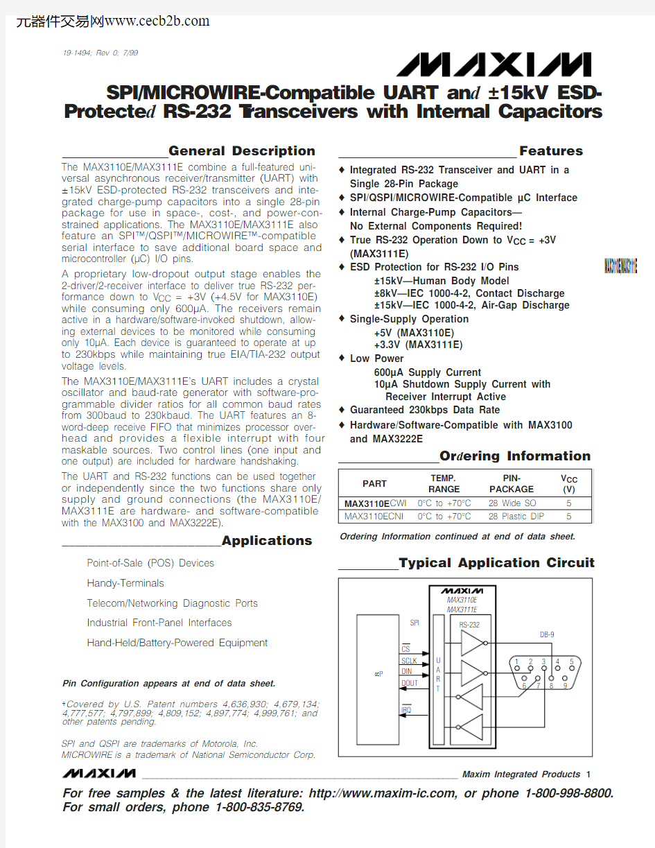
The MAX3110E/MAX3111E combine a full-featured uni-versal asynchronous receiver/transmitter (UART) with ±15kV ESD-protected RS-232 transceivers and inte-grated charge-pump capacitors into a single 28-pin package for use in space-, cost-, and power-con-strained applications. The MAX3110E/MAX3111E also feature an SPI?/QSPI?/MICROWIRE?-compatible serial interface to save additional board space and microcontroller (μC) I/O pins.
A proprietary low-dropout output stage enables the 2-driver/2-receiver interface to deliver true RS-232 per-formance down to V CC = +3V (+4.5V for MAX3110E)while consuming only 600μA. The receivers remain active in a hardware/software-invoked shutdown, allow-ing external devices to be monitored while consuming only 10μA. Each device is guaranteed to operate at up to 230kbps while maintaining true EIA/TIA-232 output voltage levels.
The MAX3110E/MAX3111E’s UART includes a crystal oscillator and baud-rate generator with software-pro-grammable divider ratios for all common baud rates from 300baud to 230kbaud. The UART features an 8-word-deep receive FIFO that minimizes processor over-head and provides a flexible interrupt with four maskable sources. Two control lines (one input and one output) are included for hardware handshaking.The UART and RS-232 functions can be used together or independently since the two functions share only supply and ground connections (the MAX3110E/MAX3111E are hardware- and software-compatible with the MAX3100 and MAX3222E).
________________________Applications
Point-of-Sale (POS) Devices Handy-Terminals
Telecom/Networking Diagnostic Ports Industrial Front-Panel Interfaces Hand-Held/Battery-Powered Equipment
Features
o Integrated RS-232 Transceiver and UART in a Single 28-Pin Package
o SPI/QSPI/MICROWIRE-Compatible μC Interface o Internal Charge-Pump Capacitors—No External Components Required!
o True RS-232 Operation Down to V CC = +3V (MAX3111E)
o ESD Protection for RS-232 I/O Pins
±15kV—Human Body Model
±8kV—IEC 1000-4-2, Contact Discharge ±15kV—IEC 1000-4-2, Air-Gap Discharge
o Single-Supply Operation
+5V (MAX3110E)+3.3V (MAX3111E)
o Low Power
600μA Supply Current
10μA Shutdown Supply Current with Receiver Interrupt Active
o Guaranteed 230kbps Data Rate
o Hardware/Software-Compatible with MAX3100and MAX3222E
MAX3110E/MAX3111E ?
SPI/MICROWIRE-Compatible UART and ±15kV ESD-Protected RS-232 T ransceivers with Internal Capacitors
________________________________________________________________Maxim Integrated Products 1
19-1494; Rev 0; 7/99
Typical Application Circuit
Ordering Information
SPI and QSPI are trademarks of Motorola, Inc.
MICROWIRE is a trademark of National Semiconductor Corp.
Ordering Information continued at end of data sheet.
Pin Configuration appears at end of data sheet.
?Covered by U.S. Patent numbers 4,636,930; 4,679,134;
4,777,577; 4,797,899; 4,809,152; 4,897,774; 4,999,761; and other patents pending.
M A X 3110E /M A X 3111E
SPI/MICROWIRE-Compatible UART and ±15kV ESD-Protected RS-232 T ransceivers with Internal Capacitors
2
_______________________________________________________________________________________
ABSOLUTE MAXIMUM RATINGS
ELECTRICAL CHARACTERISTICS—MAX3110E
(V CC = +4.5V to +5.5V, T A = T MIN to T MAX , unless otherwise noted. Typical values are measured for baud rate set to 9600baud at V CC = +5V, T A = +25°C.) (Note 2)
Stresses beyond those listed under “Absolute Maximum Ratings” may cause permanent damage to the device. These are stress ratings only, and function-al operation of the device at these or any other conditions beyond those indicated in the operational sections of the specifications is not implied. Exposure to absolute maximum rating conditions for extended periods may affect device reliability.
V CC to GND (MAX3110E)........................................-0.3V to +6V V CC to GND (MAX3111E).........................................-0.3V to +4V V+ to GND (Note 1)..................................................-0.3V to +7V V- to GND (Note 1)...................................................+0.3V to -7V V+ to V- (Note 1)..................................................................+13V Input Voltages to GND
CS , X1, CTS , RX, DIN, SCLK..................-0.3V to (V CC + 0.3V)T_IN, SHDN ...........................................................-0.3V to +6V R_IN..................................................................................±25V Output Voltage to GND
DOUT, RTS , TX, X2 .................................-0.3V to (V CC + 0.3V)IRQ .......................................................................-0.3V to +6V T_OUT ...........................................................................±13.2V R_OUT.....................................................-0.3V to (V CC + 0.3V)
TX, RTS Output Current....................................................100mA Short-Circuit Duration
X2, DOUT, IRQ (to V CC or GND).............................Continuous T_OUT (to GND) .....................................................Continuous Continuous Power Dissipation (T A = +70°C)
28-pin Wide SO (derate 12.5mW/°C above +70°C) ...........1W 28-pin Plastic DIP (derate 14.3mW/°C above +70°C)....1.14W Operating Temperature Ranges
MAX311_EC_ _ ..................................................0°C to +70°C MAX311_EE_ _ ................................................-40°C to +85°C Storage Temperature Range ............................-65°C to +150°C Lead Temperature (soldering, 10sec).............................+300°C
Note 1:V+ and V- can have maximum magnitudes of 7V, but their absolute difference should not exceed 13V.
MAX3110E/MAX3111E
SPI/MICROWIRE-Compatible UART and ±15kV ESD-Protected RS-232 T ransceivers with Internal Capacitors
_______________________________________________________________________________________3
ELECTRICAL CHARACTERISTICS—MAX3110E (continued)
(V CC = +4.5V to +5.5V, T A = T MIN to T MAX , unless otherwise noted. Typical values are measured for baud rate set to 9600baud at V CC = +5V, T A = +25°C.) (Note 2)
M A X 3110E /M A X 3111E
SPI/MICROWIRE-Compatible UART and ±15kV ESD-Protected RS-232 T ransceivers with Internal Capacitors
4_______________________________________________________________________________________
ELECTRICAL CHARACTERISTICS—MAX3110E (continued)
(V CC = +4.5V to +5.5V, T A = T MIN to T MAX , unless otherwise noted. Typical values are measured for baud rate set to 9600baud at V CC = +5V, T A = +25°C.) (Note 2)
SPI/MICROWIRE-Compatible UART and ±15kV ESD-Protected RS-232 T ransceivers with Internal Capacitors
_______________________________________________________________________________________5MAX3110E/MAX3111E
ELECTRICAL CHARACTERISTICS—MAX3111E
(V CC= +3.0V to +3.6V, V A = T MIN to T MAX, unless otherwise noted. Typical values are measured for baud rate set to 9600baud at V CC= +3.3V, T A= +25°C.) (Note 2)
M A X 3110E /M A X 3111E
SPI/MICROWIRE-Compatible UART and ±15kV ESD-Protected RS-232 T ransceivers with Internal Capacitors
6_______________________________________________________________________________________
ELECTRICAL CHARACTERISTICS—MAX3111E (continued)
(V CC = +3.0V to +3.6V, V A = T MIN to T MAX , unless otherwise noted. Typical values are measured for baud rate set to 9600baud at V CC = +3.3V, T A = +25°C.) (Note 2)
MAX3110E/MAX3111E SPI/MICROWIRE-Compatible UART and ±15kV ESD-Protected RS-232 T ransceivers with Internal Capacitors _______________________________________________________________________________________7 ELECTRICAL CHARACTERISTICS—MAX3111E (continued)
(V CC= +3.0V to +3.6V, V A = T MIN to T MAX, unless otherwise noted. Typical values are measured for baud rate set to 9600baud at
V CC= +3.3V, T= +25°C.) (Note 2)
Note 2:All currents into the device are positive; all currents out of the device are negative. All voltages are referred to device ground unless otherwise noted.
Note 3:I CCSHDN(H)represents a hardware-only shutdown. In hardware shutdown, the UART is in normal operation and the charge pumps for the RS-232 transmitters are shut down.
Note 4:I CCSHDN(H+S)represents a simultaneous software and hardware shutdown in which the UART and charge pumps are shut down.
Note 5:Transmitter skew is measured at the transmitter zero cross points.
M A X 3110E /M A X 3111E
SPI/MICROWIRE-Compatible UART and ±15kV ESD-Protected RS-232 T ransceivers with Internal Capacitors
8_______________________________________________________________________________________
010
5153035402520500
1000
2000
3000
4000
5000
RS-232 TRANSCEIVER SUPPLY CURRENT
vs. LOAD CAPACITANCE
LOAD CAPACITANCE (pF)
S U P P L Y C U R R E N T (m A )
45
04
26121410816
1000
2000
3000
4000
5000
RS-232 TRANSMITTER SLEW RATE
vs. LOAD CAPACITANCE
LOAD CAPACITANCE (pF)
S L E W R A T E (V /μs )
-10.0
-5.0-7.5-2.55.07.52.5010.00
1000
2000
3000
4000
5000
RS-232 TRANSMITTER OUTPUT VOLTAGE
vs. LOAD CAPACITANCE
LOAD CAPACITANCE (pF)T R A N S M I T T E R O U T P U T V O L T A G E (V )
Typical Operating Characteristics
(T
A = +25°C, unless otherwise noted.)
10009000-40
-204060100
UART SUPPLY CURRENT vs. TEMPERATURE
200100800700TEMPERATURE (°C)
S U P P L Y C U R R E N T (μA )
02080600500400300109
0-40
-20
40
60
100
UART SHUTDOWN CURRENT
vs. TEMPERATURE
21
8
7TEMPERATURE (°C)
S H U T D O W N C U R R E N T (μA )
20
80
654340050
10010k 1000100k
1M
UART SUPPLY CURRENT
vs. BAUD RATE
150100
BAUD RATE (bps)
S U P P L Y C U R R E N T (μA )
200250350300
7006000
1
3
4
5
UART SUPPLY CURRENT vs. EXTERNAL CLOCK FREQUENCY
100500EXTERNAL CLOCK FREQUENCY (MHz)
S U P P L Y C U R R E N T (μA )
2
400300200
70
00.20.10.60.70.8 1.0
MAX3111E
TX, RTS, DOUT OUTPUT CURRENT vs. OUTPUT LOW VOLTAGE (V CC = +3.3V)
10VOLTAGE (V)
O U T P U T S I N K C U R R E N T (m A )
0.30.50.40.96050403020
90800
00.20.10.60.70.8 1.0
MAX3110E
TX, RTS, DOUT OUTPUT CURRENT vs. OUTPUT LOW VOLTAGE (V CC = +5V)
1070VOLTAGE (V)
O U T P U T S I N K C U R R E N T (m A )
0.30.50.40.96050403020
MAX3110E/MAX3111E
SPI/MICROWIRE-Compatible UART and ±15kV ESD-Protected RS-232 T ransceivers with Internal Capacitors
_______________________________________________________________________________________9
Pin Description
M A X 3110E /M A X 3111E
SPI/MICROWIRE-Compatible UART and ±15kV ESD-Protected RS-232 T ransceivers with Internal Capacitors
10
______________________________________________________________________________________
Detailed Description
The MAX3110E/MAX3111E contain an SPI/QSPI/MICROWIRE-compatible UART and an RS-232 transceiver with two drivers and two receivers. The UART is compatible with SPI and QSPI for CPOL = 0 and CPHA = 0. The UART supports data rates up to 230kbaud for standard UART bit streams as well as IrDA and includes an 8-word receive FIFO. Also included is a 9-bit-address recogni-tion interrupt.
The RS-232 transceiver has electrostatic discharge (ESD) protection on the transmitter outputs and the receiver inputs. The internal charge-pump capacitors minimize the number of external components required.The RS-232 transceivers meet EIA/TIA-232 specifica-tions for V CC down to the minimum supply voltage and are guaranteed to operate for data rates up to 250kbps. The UART and RS-232 functions operate as one device or independently since the two functions share only supply and ground connections.
UART
The universal asynchronous receiver transmitter (UART) interfaces the SPI/QSPI/MICROWIRE-compati-ble synchronous serial data from a microprocessor (μP)to asynchronous, serial-data communication ports (RS-232, IrDA). Figure 1 shows the MAX3110E/MAX3111E functional diagram. Included in the UART function is an SPI/QSPI/MICROWIRE interface, a baud-rate generator,and an interrupt generator.
Figure 1. MAX3110E/MAX3111E Functional Diagram
MAX3110E/MAX3111E
SPI/MICROWIRE-Compatible UART and ±15kV ESD-Protected RS-232 T ransceivers with Internal Capacitors
______________________________________________________________________________________11
SPI Interface
The MAX3110E/MAX3111E are compatible with SPI,QSPI (CPOL = 0, CPHA = 0), and MICROWIRE serial-interface standards (Figure 2). The MAX3110E/MAX3111E have a unique full-duplex-only architecture that expects a 16-bit word for DIN and simultaneously produces a 16-bit word for DOUT regardless of which read/write register is used. The DIN stream is moni-tored for its first two bits to tell the UART the type of data transfer being executed (see the Write Configuration Register , Read Configuration Register ,Write Data Register , and Read Data Registe r sections).DIN (MOSI) is latched on SCLK’s rising edge. DOUT (MISO) should be read into the μP on SCLK’s rising edge. The first bit (bit 15) of DOUT transitions on CS ’s falling edge, and bits 14–0 transition on SCLK’s falling
edge. Figure 3 shows the detailed serial timing specifi-cations for the synchronous SPI port.
Only 16-bit words are expected. If CS goes high in the middle of a transmission (any time before the 16th bit),the sequence is aborted (i.e., data does not get written to individual registers). Most operations, such as the clearing of internal registers, are executed only on CS ’s rising edge. Every time CS goes low, a new 16-bit stream is expected. An example of using the Write Configuration Register is shown in Figure 4.
Table 1 describes the bits located in the Write Config-uration, Read Configuration, Write Data, and Read Data Registers. This table also describes whether the bit is a read or a write bit and the power-on reset state (POR) of the bits. Figure 5 shows an example of parity and word-length control.
CS SCLK
SCLK
SCLK
SCLK
(CPOL = 0, CPHA = 0)(CPOL = 0, CPHA = 1)(CPOL = 1, CPHA = 0)(CPOL = 1, CPHA = 1)
COMPATIBLE
WITH MAX3110E/MAX3111E
NOT COMPATIBLE
WITH MAX3110E/MAX3111E
DIN MSB 1314121110987654321LSB DOUT MSB
13
14
12
11
10
9
8
7
6
5
4
3
2
1
LSB
Figure 2. Compatible CPOL and CPHA Timing Modes
Figure 3. Detailed Serial Timing Specifications for the Synchronous SPI Port
M A X 3110E /M A X 3111E
12______________________________________________________________________________________
SPI/MICROWIRE-Compatible UART and ±15kV ESD-Protected RS-232 T ransceivers with Internal Capacitors
Figure 4. Write Configuration Register Example
Figure 5. Parity and Word-Length Control
MAX3110E/MAX3111E
SPI/MICROWIRE-Compatible UART and ±15kV ESD-Protected RS-232 T ransceivers with Internal Capacitors
______________________________________________________________________________________13
M A X 3110E /M A X 3111E
SPI/MICROWIRE-Compatible UART and ±15kV ESD-Protected RS-232 T ransceivers with Internal Capacitors
14
______________________________________________________________________________________
Notice to High-Level Programmers:The UART follows the SPI convention of providing a bidirectional data path for writes and reads. Whenever the data is written, data is also read back. This speeds operation over the SPI bus, and the UART needs this speed advantage when operating at high baud rates. In most high-level lan-guages, such as C, there are commands for writing and reading stream I/O devices such as the console or serial port. In C specifically, there is a “PUTCHAR” command that transmits a character and a “GETCHAR” command that receives a character. If programmers were to write direct write and read commands in C with no underlying driver code, they would notice that a PUTCHAR com-mand is really a PUTGETCHAR command. These C commands assume some form of BIOS-level support for these commands. The proper way to implement these commands is to write driver code, usually in the form of an assembly-language interrupt-service routine and a callable routine used by high-level routines. This driver
handles the interrupts and manages the receive and transmit buffers for the MAX3110E/MAX3111E. When a PUTCHAR executes, this driver is called and it safely buffers any characters received when the current character is transmitted. When a GETCHAR executes, it checks its own receive buffer before getting data from the UART. See the C-language Outline of a MAX3110E/MAX3111E Software Driver in Listing 1, which appears at the end of this data sheet.
Listing 1 is a C-language outline of an interrupt-driven software driver that interfaces to a MAX3110E/MAX3111E, providing an intermediate layer between the bit-manipulation subroutine and the familiar PUTCHAR/GETCHAR subroutines.
The user must supply code for managing the transmit and receive queues as well as the low-level hardware interface itself. The interrupt control hardware must be initialized before this driver is called.
Table 1. Bit Descriptions (continued)
MAX3110E/MAX3111E
SPI/MICROWIRE-Compatible UART and ±15kV ESD-Protected RS-232 T ransceivers with Internal Capacitors
______________________________________________________________________________________15
Write Configuration Register (D15, D14 = 1, 1)
Configure the UART by writing a 16-bit word to the write configuration register, which programs the baud rate,data word length, parity enable, and enable of the 8-word receive FIFO. In this mode, bits 15 and 14 of the DIN configuration word are both required to be 1 in order to enable the write configuration mode. Bits 13–0of the DIN configuration word set the configuration of the UART. Table 2 shows the bit assignment for the write configuration register. The write configuration reg-ister allows selection between normal UART timing and IrDA timing, provides shutdown control, and contains four interrupt mask bits.
Using the write configuration register clears the receive FIFO and the R, T, RA/FE, D0r–D7r, D0t–D7t, Pr, and Pt registers. RTS and CTS remain unchanged. The new configuration is valid on CS ’s rising edge if the transmit buffer is empty (T = 1) and transmission is over. If the latest transmission has not been completed (T = 0), the registers are updated when the transmission is over.The write configuration register bits (FEN , SHDNi, IR,ST, PE, L, B3–B0) take effect after the current transmis-sion is over. The mask bits (TM , RM , PM , RAM ) take effect immediately after SCLK’s 16th rising edge.
Bits 15 and 14 of the DOUT write configuration (R and T) are sent out of the MAX3110E/MAX3111E along with 14 trailing zeros. The use of the R and T bits is optional,but ignore the 14 trailing zeros.
Warning!The UART requires stable crystal oscillator operation before configuration (typically ~25ms after power-up). Upon power-up, compare the write configu-ration bits with the read configuration bits in a software loop until both match. This ensures that the oscillator is stable and that the UART is configured correctly.Read Configuration Mode (D15, D14 = 0, 1)
The read configuration mode is used to read back the last configuration written to the UART. In this mode, bits 15 and 14 of the DIN configuration word are required to be 0 and 1, respectively, to enable the read configura-tion mode. Bits 13–1 of the DIN word should be zeros,and bit 0 is the test bit to put the UART in test mode (see the Test Mode section). Table 3 shows the bit assignment for the read configuration register.
Test Mode
The device enters a test mode if bit 0 of the DIN config-uration word equals one when doing a read configura-tion. In this mode, if CS = 0, the RTS pin transmits a clock that is 16-times the baud rate. The TX pin is low as long as CS remains low while in test mode. Table 3shows the bit assignment for the read configuration register.
Write Data Register (D15, D14 = 1, 0)
Use the write data register for transmitting to the TX-buffer and receiving from the RX buffer (and RX FIFO when enabled). When using this register, the DIN and DOUT write data words are used simultaneously, and bits 13–11 for both the DIN and DOUT write data words are meaningless zeros. The DIN write data word con-tains the data that is being transmitted, and the DOUT write data word contains the data that is being received from the RX FIFO. Table 4 shows the bit assignment for the write data mode. To change the RTS pin’s output state without transmitting data, set the TE bit high. If performing a write data operation, the R bit will clear on the falling edge of SCLK’s 16th clock pulse if no new data is available.
Read Data Register (D15, D14 = 0, 0)
Use the read data register for receiving data from the RX FIFO. When using this register, bits 15 and 14 of DIN are both required to be 0. Bits 13–0 of the DIN read-data word should be zeros. Table 5 shows the bit assignments for the read data mode. Reading data clears the R bit and interrupt IRQ . If performing a read data operation, the R bit will clear on the falling edge of SCLKs 16th clock pulse if no new data is available.
M A X 3110E /M A X 3111E
SPI/MICROWIRE-Compatible UART and ±15kV ESD-Protected RS-232 T ransceivers with Internal Capacitors
16______________________________________________________________________________________
Table 2. Write Configuration (D15, D14 = 1, 1)
Notes:
bit 15: DOUT
R = 1, Data is available to be read or is being read from the receive register or FIFO.
R = 0, Receive register and FIFO are empty.bit 14: DOUT
T = 1, Transmit buffer is empty.T = 0, Transmit buffer is full.bits 13–0: DOUT Zeros
bits 15, 14: DIN
1,1 = Write Configuration bit 13: DIN
FEN = 0, FIFO is enabled.FEN = 1, FIFO is disabled.bit 12: DIN
SHDNi = 1, Enter software shutdown.SHDNi = 0, Exit software shutdown.bit 11: DIN
TM = 1, Transmit buffer empty interrupt is enabled.TM = 0, Transmit buffer empty interrupt is disabled.bit 10: DIN
RM = 1, Data available in the receive register or FIFO interrupt is enabled.
RM = 0, Data available in the receive register or FIFO interrupt is disabled.bit 9: DIN
PM = 1, Parity bit high received interrupt is enabled.PM = 0, Parity bit received interrupt is disabled.bit 8: DIN
RAM = 1, Receiver-activity (shutdown mode)/Framing-error (normal operation) interrupt is enabled.
RAM = 0, Receiver-activity (shutdown mode)/Framing-error (normal operation) interrupt is disabled.
bit 7: DIN
IR = 1, IrDA mode is enabled.IR = 0, IrDA mode is disabled.bit 6: DIN
ST = 1, Transmit two stop-bits.ST = 0, Transmit one stop-bit.bit 5: DIN
PE = 1, Parity is enabled for both transmit (state of Pt) and receive.
PE = 0, Parity is disabled for both transmit and receive.bit 4: DIN
L = 1, 7-bit words (8-bit words if PE = 1)L = 0, 8-bit words (9-bit words if PE = 1)bits 3–0: DIN
B3–B0 = XXXX, Baud-Rate Divisor Select Bits (see Table 6)
D15 is present at DOUT on CS ’s falling edge. Consecutive bits are clocked out on SCLK’s falling edge.
MAX3110E/MAX3111E
SPI/MICROWIRE-Compatible UART and ±15kV ESD-Protected RS-232 T ransceivers with Internal Capacitors
______________________________________________________________________________________
17
Table 3. Read Configuration (D15, D14 = 0, 1)
Notes:
bit 15: DOUT
R = 1, Data is available to be read or is being read from the receive register or FIFO.
R = 0, Receive register and FIFO are empty.bit 14: DOUT
T = 1, Transmit buffer is empty.T = 0, Transmit buffer is full.bit 13: DOUT
FEN = 0, FIFO is enabled.FEN = 1, FIFO is disabled.bit 12: DOUT
SHDNo = 1, Software shutdown is enabled.SHDNo = 0, Software shutdown is disabled.bit 11: DOUT
TM = 1, Transmit buffer empty interrupt is enabled.TM = 0, Transmit buffer empty interrupt is disabled.bit 10: DOUT
RM = 1, Data available in the receive register or FIFO interrupt is enabled.
RM = 0, Data available in the receive register or FIFO interrupt is disabled.bit 9: DOUT
PM = 1, Parity bit high received interrupt is enabled.PM = 0, Parity bit received interrupt is disabled.bit 8: DOUT
RAM = 1, Receiver-activity (shutdown mode)/Framing-error (normal operation) interrupt is enabled.
RAM = 0, Receiver-activity (shutdown mode)/Framing-error (normal operation) interrupt is disabled.bit 7: DOUT
IR = 1, IrDA mode is enabled.IR = 0, IrDA mode is disabled.bit 6: DOUT
ST = 1, Transmit two stop-bits.ST = 0, Transmit one stop-bit.bit 5: DOUT
PE = 1, Parity is enabled for both transmit (state of Pt) and receive.
PE = 0, Parity is disabled for both transmit and receive.bit 4: DOUT
L = 1, 7-bit words (8-bit words if PE = 1)L = 0, 8-bit words (9-bit words if PE = 1)
bits 3–0: DOUT
B3–B0 = XXXX Baud-Rate Divisor Select Bits (see Table 6)
bit 15, 14: DIN
0,1 = Read Configuration bits 13–1: DIN Zeros
bit 0: DIN
If TEST = 1 and CS = 0, then RTS =16xBaudCLK TEST = 0, Disables test mode
D15 is present at DOUT on CS ’s falling edge. Consecutive bits are clocked out on SCLK’s falling edge.
M A X 3110E /M A X 3111E
SPI/MICROWIRE-Compatible UART and ±15kV ESD-Protected RS-232 T ransceivers with Internal Capacitors
18______________________________________________________________________________________
Table 4. Write Data (D15, D14 = 1, 0)
Notes:bit 15: DOUT
R = 1, Data is available to be read or is being read from the receive register or FIFO.
R = 0, Receive register and FIFO are empty.bit 14: DOUT
T = 1, Transmit buffer is empty.T = 0, Transmit buffer is full.bits 13–11: DOUT Zeros bit 10: DOUT
RA/FE = Receive-Activity (Uart shutdown)/Framing-Error (Normal Operation) bit bit 9: DOUT
CTS = CTS input state. If CTS = 0, then CTS = 1 and vice versa.bit 8: DOUT
Pr = Received Parity Bit. This is only valid if PE = 1. bits 7–0: DOUT
D7t–D0t = Received Data Bits. D7r = 0 for L = 1.
bits 15, 14: DIN 1, 0 = Write Data bits 13–11: DIN Zeros bit 10: DIN
TE = 1, Disables transmit and only RTS will be updated.TE = 0, Enables transmit.bit 9: DIN
RTS = 1, Configures RTS = 0 (logic low).RTS = 0, Configures RTS = 1 (logic high).bit 8: DIN
Pt = 1, Transmit parity bit is high. If PE = 1, a high parity bit will be transmitted. If PE = 0, then no parity bit will be transmitted.Pt = 0, Transmit parity bit is low. If PE = 1, a low parity bit will be transmitted. If PE = 0, then no parity bit will be transmitted.bits 7–0: DIN
D7t–D0t = Transmitting Data Bits. D7t is ignored when L = 1.
D15 is present at DOUT on CS ’s falling edge. Consecutive bits are clocked out on SCLK’s falling edge.
MAX3110E/MAX3111E
SPI/MICROWIRE-Compatible UART and ±15kV ESD-Protected RS-232 T ransceivers with Internal Capacitors
______________________________________________________________________________________19
Table 5. Read Data (D15, D14 = 0, 0)
Notes:bits 15: DOUT
R = 1, Data is available to be read or is being read from the receive register or FIFO.
R = 0, Receive register and FIFO are empty.bit 14: DOUT
T = 1, Transmit buffer is empty.T = 0, Transmit buffer is full.bits 13–11: DOUT Zeros bit 10: DOUT
RA/FE = Receive-Activity (UART shutdown)/Framing-Error (Normal Operation) Bit bit 9: DOUT
CTS = CTS input state. If CTS = 0, then CTS = 1 and vice versa.bit 8: DOUT
Pr = Received parity bit. This is only valid if PE = 1. bits 7–0: DOUT
D7t–D0t = Received Data Bits. D7r = 0 for L = 1.
bits 15, 14: DIN 0, 0 = Read Data bits 13–0: DIN Zeros
D15 is present at DOUT on CS ’s falling edge. Consecutive bits are clocked out on SCLK’s falling edge.
M A X 3110E /M A X 3111E
SPI/MICROWIRE-Compatible UART and ±15kV ESD-Protected RS-232 T ransceivers with Internal Capacitors
20______________________________________________________________________________________
Baud-Rate Generator
The baud-rate generator determines the rate at which the transmitter and receiver operate. Bits B3–B0 in the write configuration register determine the baud-rate divisor (BRD), which divides the X1 oscillator frequen-cy. The on-board oscillator operates with either a 1.8432MHz or a 3.6864MHz crystal or is driven at X1with a 45% to 55% duty-cycle square wave. Table 6shows baud-rate divisors for given input codes as well as the baud rate for 1.8432MHz and 3.684MHz crystals.The generator’s clock is 16-times the baud rate.Interrupt Sources and Masks
Using the Read Data or Write Data register clears the interrupt IRQ,assuming the conditions that initiated the interrupt no longer exist. Table 7 gives the details for each interrupt source. Figure 6 shows the functional diagram for the interrupt sources and mask blocks.
Following are two examples of setting up an IRQ for the MAX3110E/MAX3111E:
Example 1.Set up only the transmit buffer-empty inter-rupt. Send the 16-bit word below into DIN of the MAX3110E/MAX3111E using the Write Configuration register. This 16-bit word configures the MAX3110E/MAX3111E for 9600bps, 8-bit words, no parity, and one stop bit with a 1.8432MHz crystal.
binary 1100100000001010HEX C80A
Example 2.Set up only the data-available (or data-being-read) interrupt.
Send the 16-bit word below into DIN of the MAX3110E/MAX3111E using the Write Configuration register. This 16-bit word configures the MAX3110E/MAX3111E for 9600bps, 8-bit words, no parity, and one stop bit with a 1.8432MHz crystal.
binary 1100010000001010HEX C40A
Receive FIFO
The MAX3110E/MAX3111E contain an 8-word receive FIFO for data received by the UART to minimize processor overhead. Using the UART-software shut-down clears the receive FIFO. Upon power-up, the receive FIFO is enabled. To disable the receive FIFO,set the FEN bit high when writing to the Write Configuration register. To check whether the FIFO is enabled or disabled, read back the FEN bit using the Read Configuration.
Figure 6. Functional Diagram for Interrupt Sources and Mask Blocks
*Standard baud rates shown in bold **Default baud rate