UCC1800/1/2/3/4/5UCC2800/1/2/3/4/5UCC3800/1/2/3/4/5
FEATURES
?100μA Typical Starting Supply Current ?500μA Typical Operating Supply Current
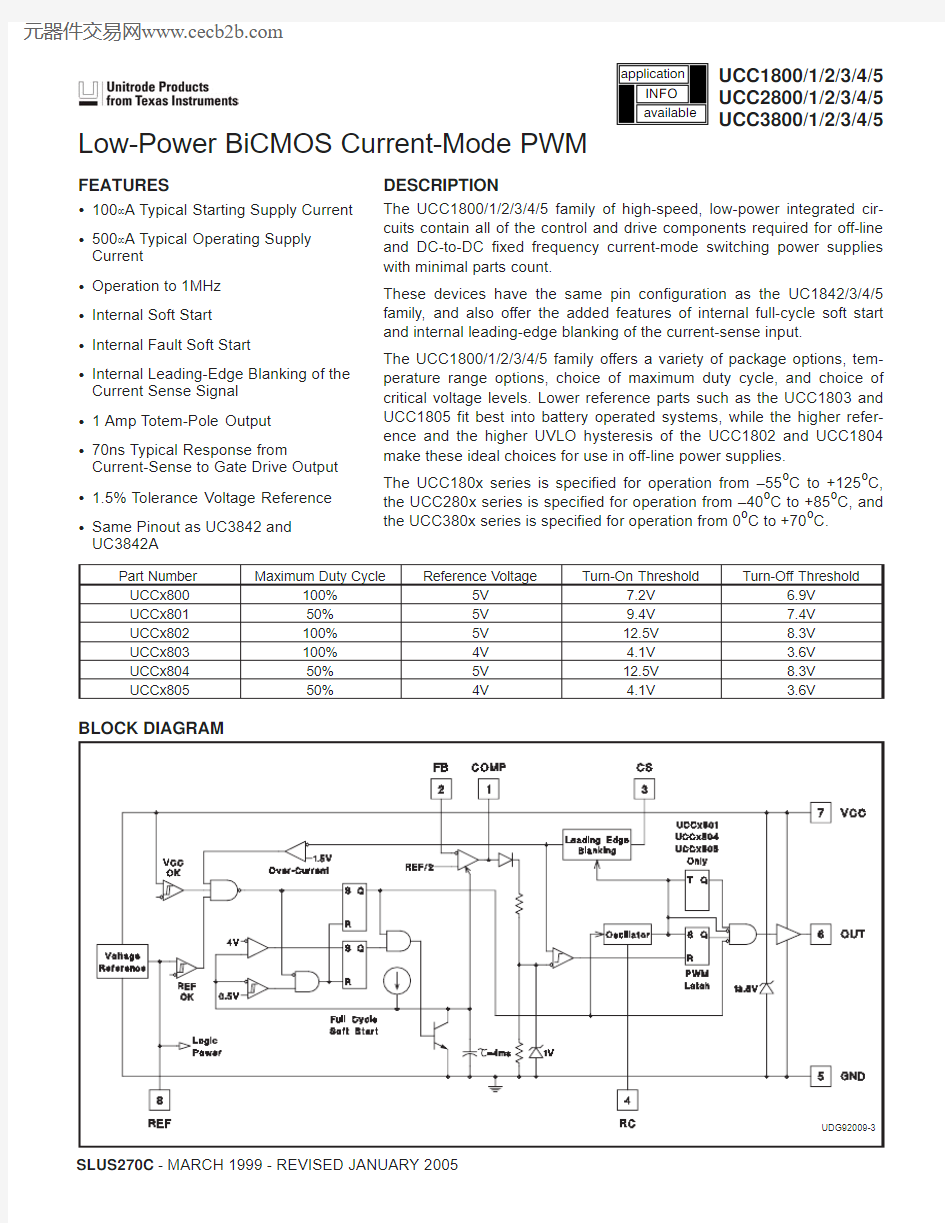
?Operation to 1MHz ?Internal Soft Start ?Internal Fault Soft Start
?Internal Leading-Edge Blanking of the Current Sense Signal ?1Amp Totem-Pole Output
?70ns Typical Response from
Current-Sense to Gate Drive Output ?1.5%Tolerance Voltage Reference ?Same Pinout as UC3842and UC3842A
DESCRIPTION
The UCC1800/1/2/3/4/5family of high-speed,low-power integrated cir-cuits contain all of the control and drive components required for off-line and DC-to-DC fixed frequency current-mode switching power supplies with minimal parts count.
These devices have the same pin configuration as the UC1842/3/4/5family,and also offer the added features of internal full-cycle soft start and internal leading-edge blanking of the current-sense input.
The UCC1800/1/2/3/4/5family offers a variety of package options,tem-perature range options,choice of maximum duty cycle,and choice of critical voltage levels.Lower reference parts such as the UCC1803and UCC1805fit best into battery operated systems,while the higher refer-ence and the higher UVLO hysteresis of the UCC1802and UCC1804make these ideal choices for use in off-line power supplies.
The UCC180x series is specified for operation from –55o
C to +125o
C,
the UCC280x series is specified for operation from –40o C to +85o
C,and
the UCC380x series is specified for operation from 0o C to +70o
C.
Low-Power BiCMOS Current-Mode PWM
Part Number Maximum Duty Cycle
Reference Voltage
Turn-On Threshold
Turn-Off Threshold
UCCx800100%5V
7.2V 6.9V UCCx80150%5V 9.4V 7.4V UCCx802100%5V 12.5V 8.3V UCCx803100%4V 4.1V 3.6V UCCx80450%5V 12.5V 8.3V UCCx805
50%4V 4.1V 3.6V
BLOCK DIAGRAM
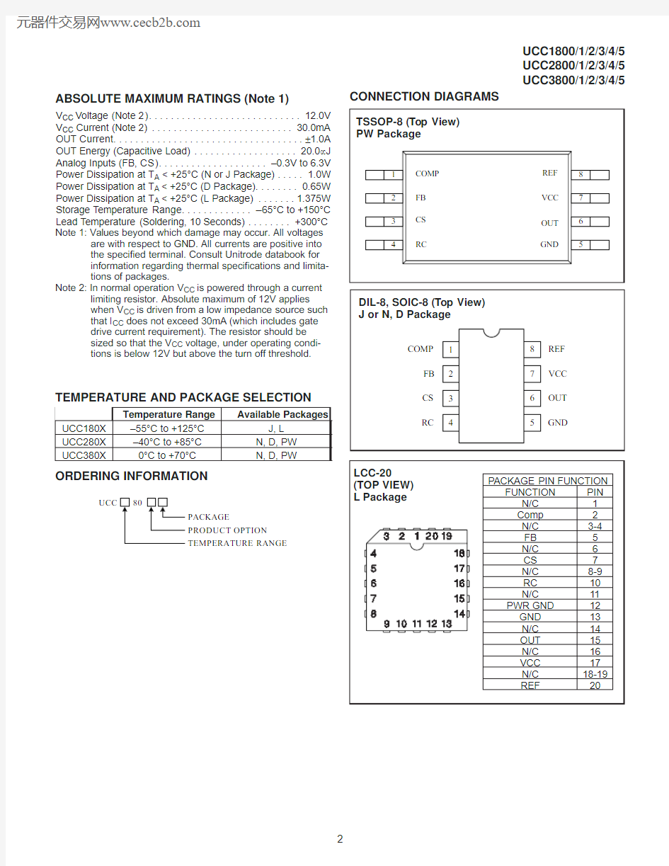
DIL-8,SOIC-8(Top View)J or N,D Package
OUT VCC REF GND
1234
8765
FB
COMP
CS RC
ABSOLUTE MAXIMUM RATINGS (Note 1)
V CC Voltage (Note 2)............................12.0V V CC Current (Note 2)..........................30.0mA OUT Current...................................±1.0A OUT Energy (Capacitive Load)...................20.0μJ Analog Inputs (FB,CS)....................–0.3V to 6.3V Power Dissipation at T A <+25°C (N or J Package)..... 1.0W Power Dissipation at T A <+25°C (D Package)........0.65W Power Dissipation at T A <+25°C (L Package).......1.375W Storage Temperature Range.............–65°C to +150°C Lead Temperature (Soldering,10Seconds)........+300°C Note 1:Values beyond which damage may occur.All voltages
are with respect to GND.All currents are positive into the specified terminal.Consult Unitrode databook for information regarding thermal specifications and limita-tions of packages.
Note 2:In normal operation V CC is powered through a current
limiting resistor.Absolute maximum of 12V applies when V CC is driven from a low impedance source such that I CC does not exceed 30mA (which includes gate drive current requirement).The resistor should be sized so that the V CC voltage,under operating condi-tions is below 12V but above the turn off threshold.
CONNECTION DIAGRAMS
UCC
PRODUCT OPTION PACKAGE
TEMPERATURE RANGE
ORDERING INFORMATION
Temperature Range Available Packages
UCC180X –55°C to +125°C J,L UCC280X –40°C to +85°C N,D,PW UCC380X
0°C to +70°C
N,D,PW
TEMPERATURE AND PACKAGE SELECTION
ELECTRICAL CHARACTERISTICS Unless otherwise stated,these specifications apply for–55°C≤T A≤+125°C for UCC180x;–40°C≤T A≤+85°C for UCC280x;0°C≤T A≤+70°C for UCC380x;V CC=10V(Note3);RT=100k from REF to RC;
CT=330pF from RC to GND;0.1F capacitor from V CC to GND;0.1F capacitor from V REF to GND.T A=T J.
UCC380X UNITS PARAMETER TEST CONDITIONS UCC180X
UCC280X
MIN TYP MAX MIN TYP MAX Reference Section
Output Voltage T J=+25°C,I=0.2mA,UCCx800/1/2/4 4.925 5.00 5.075 4.925 5.00 5.075V
T J=+25°C,I=0.2mA,UCCx803/5 3.94 4.00 4.06 3.94 4.00 4.06 Load Regulation0.2mA 1.9 1.9mV/V Line Regulation T J=+25°C, V CC=10V to Clamp(I VCC=25mA) 2.5 2.1mV/V T J=–55°C to+125°C, V CC=10V to Clamp(I VCC=25mA) Total Variation UCCx800/1/2/4(Note7) 4.88 5.00 5.10 4.88 5.00 5.10V UCCx803/5(Note7) 3.90 4.00 4.08 3.90 4.00 4.08V Output Noise Voltage10Hz≤f≤10kHz,T J=+25°C(Note9)130130μV Long Term Stability T A=+125°C,1000Hours(Note9)55mV Output Short Circuit–5–35–5–35mA Oscillator Section Oscillator Frequency UCCx800/1/2/4(Note4)404652404652kHz UCCx803/5(Note4)263136263136kHz Temperature Stability(Note9) 2.5 2.5% Amplitude peak-to-peak 2.25 2.40 2.55 2.25 2.40 2.55V Oscillator Peak Voltage 2.45 2.45V Error Amplifier Section Input Voltage COMP=2.5V;UCCx800/1/2/4 2.44 2.50 2.56 2.44 2.50 2.56V COMP=2.0V;UCCx803/5 1.95 2.0 2.05 1.95 2.0 2.05 Input Bias Current–11–11μA Open Loop Voltage Gain60806080dB COMP Sink Current FB=2.7V,COMP=1.1V0.3 3.50.4 2.5mA COMP Source Current FB=1.8V,COMP=REF–1.2V–0.2–0.5–0.8–0.2–0.5–0.8mA Gain Bandwidth Product(Note9)22MHz PWM Section Maximum Duty Cycle UCCx800/2/397991009799100% UCCx801/4/5484950484950 Minimum Duty Cycle COMP=0V00% Current Sense Section Gain(Note5) 1.10 1.65 1.80 1.10 1.65 1.80V/V Maximum Input Signal COMP=5V(Note6)0.9 1.0 1.10.9 1.0 1.1V Input Bias Current–200200–200200nA CS Blank Time5010015050100150ns Over-Current Threshold 1.42 1.55 1.68 1.42 1.55 1.68V COMP to CS Offset CS=0V0.450.90 1.350.450.90 1.35V ELECTRICAL CHARACTERISTICS Unless otherwise stated,these specifications apply for –55°C ≤T A ≤+125°C for UCC180x;–40°C ≤T A ≤+85°C for UCC280x;0°C ≤T A ≤+70°C for UCC380x;V CC =10V (Note 3);RT=100k from REF to RC;CT=330pF from RC to GND;0.1F capacitor from V CC to GND;0.1F capacitor from V REF to GND.T A =T J . PARAMETER TEST CONDITIONS UCC180X UCC280X UCC380X UNITS Output Section OUT Low Level I=20mA,all parts 0.10.40.10.4V I=200mA,all parts 0.350.900.350.90V I=50mA,VCC=5V,UCCx803/50.150.400.150.40V I=20mA,VCC=0V,all parts 0.7 1.20.7 1.2V OUT High V SAT (V CC -OUT)I=–20mA,all parts 0.150.400.150.40V I=–200mA,all parts 1.0 1.9 1.0 1.9V I=–50mA,VCC=5V,UCCx803/50.40.90.40.9V Rise Time C L =1nF 41704170ns Fall Time C L =1nF 44 75 44 75 ns Undervoltage Lockout Section Start Threshold (Note 8) UCCx800 6.67.27.8 6.67.27.8V UCCx8018.69.410.28.69.410.2V UCCx802/411.512.513.511.512.513.5V UCCx803/5 3.7 4.1 4.5 3.7 4.1 4.5V Stop Threshold (Note 8) UCCx1800 6.3 6.97.5 6.3 6.97.5V UCCx1801 6.87.48.0 6.87.48.0V UCCx802/47.68.39.07.68.39.0V UCCx803/5 3.2 3.6 4.0 3.2 3.6 4.0 V Undervoltage Lockout Section (cont.)Start to Stop Hysteresis UCCx8000.120.30.480.120.30.48V UCCx801 1.62 2.4 1.62 2.4V UCCx802/4 3.5 4.2 5.1 3.5 4.2 5.1V UCCx803/5 0.2 0.5 0.8 0.2 0.5 0.8 V Soft Start Section COMP Rise Time FB=1.8V,Rise from 0.5V to REF–1V 4 10 4 10 ms Overall Section Start-up Current V CC 0.5 1.00.5 1.0mA VCC Internal Zener Voltage I CC =10mA (Note 8),(Note 10) 1213.515 1213.515 V VCC Internal Zener Voltage Minus Start Threshold Voltage UCCx802/4(Note 8)0.5 1.0 0.5 1.0 V Note 3:Adjust VCC above the start threshold before setting at 10V. Note 4:Oscillator frequency for the UCCx800,UCCx802and UCCx803is the output frequency. Oscillator frequency for the UCCx801,UCCx804and UCCx805is twice the output frequency. Note 5:Gain is defined by:A V V V V COMP CS CS =≤≤??008.. Note 6:Parameter measured at trip point of latch with Pin 2at 0V. Note 7:Total Variation includes temperature stability and load regulation. Note 8:Start Threshold,Stop Threshold and Zener Shunt Thresholds track one another.Note 9:Guaranteed by design.Not 100%tested in production. Note 10:The device is fully operating in clamp mode as the forcing current is higher than the normal operating supply current. PIN DESCRIPTIONS COMP:COMP is the output of the error amplifier and the input of the PWM comparator. Unlike other devices,the error amplifier in the UCC3800 family is a true,low output-impedance,2MHz operational amplifier.As such,the COMP terminal can both source and sink current.However,the error amplifier is internally current limited,so that you can command zero duty cycle by externally forcing COMP to GND. The UCC3800family features built-in full cycle Soft Start. Soft Start is implemented as a clamp on the maximum COMP voltage. CS:CS is the input to the current sense comparators. The UCC3800family has two different current sense comparators:the PWM comparator and an over-current comparator. The UCC3800family contains digital current sense filter-ing,which disconnects the CS terminal from the current sense comparator during the100ns interval immediately following the rising edge of the OUT pin.This digital filter-ing,also called leading-edge blanking,means that in most applications,no analog filtering(RC filter)is re-quired on https://www.doczj.com/doc/fc7047952.html,pared to an external RC filter tech-nique,the leading-edge blanking provides a smaller effective CS to OUT propagation delay.Note,however, that the minimum non-zero On-Time of the OUT signal is directly affected by the leading-edge-blanking and the CS to OUT propagation delay. The over-current comparator is only intended for fault sensing,and exceeding the over-current threshold will cause a soft start cycle. FB:FB is the inverting input of the error amplifier.For best stability,keep FB lead length as short as possible and FB stray capacitance as small as possible. GND:GND is reference ground and power ground for all functions on this part. OUT:OUT is the output of a high-current power driver ca-pable of driving the gate of a power MOSFET with peak currents exceeding±750mA.OUT is actively held low when V CC is below the UVLO threshold. The high-current power driver consists of FET output de-vices,which can switch all of the way to GND and all of the way to V CC.The output stage also provides a very low impedance to overshoot and undershoot.This means that in many cases,external schottky clamp diodes are not required. RC:RC is the oscillator timing pin.For fixed frequency performance,keep the timing capacitor lead to GND as short and direct as possible.If possible,use separate ground traces for the timing capacitor and all other func-tions. The frequency of oscillation can be estimated with the following equations: UCCx800/1/2/4:F R C = ? 15. UCCx803,UCCx805:F R C = ? 10. where frequency is in Hz,resistance is in ohms,and ca-pacitance is in farads.The recommended range of timing resistors is between10k and200k and timing capacitor is 100pF to1000pF.Never use a timing resistor less than 10k. To prevent noise problems,bypass VCC to GND with a ceramic capacitor as close to the VCC pin as possible. An electrolytic capacitor may also be used in addition to the ceramic capacitor. REF:REF is the voltage reference for the error amplifier and also for many other functions on the IC.REF is also used as the logic power supply for high speed switching logic on the IC. When V CC is greater than1V and less than the UVLO threshold,REF is pulled to ground through a5k ohm re-sistor.This means that REF can be used as a logic out-put indicating power system status.It is important for reference stability that REF is bypassed to GND with a ceramic capacitor as close to the pin as possible.An electrolytic capacitor may also be used in addition to the ceramic capacitor.A minimum of0.1μF ceramic is re-quired.Additional REF bypassing is required for external loads greater than2.5mA on the reference. To prevent noise problems with high speed switching transients,bypass REF to ground with a ceramic capaci-tor very close to the IC package. VCC:V CC is the power input connection for this device. In normal operation V CC is powered through a current limiting resistor.Although quiescent V CC current is very low,total supply current will be higher,depending on OUT current.Total V CC current is the sum of quiescent V CC current and the average OUT current.Knowing the operating frequency and the MOSFET gate charge(Qg), average OUT current can be calculated from: I Q F OUT g =×. There should be a minimum of1.0m F in parallel with a 4.003.983.963.943.923.903.883.863.843.82 4 4.2 4.4 4.6 4.8 5 5.2 5.4 5.6 5.8 6 V (V)CC V (V ) R E F Figure 3.UCC1803/5V REF vs.V CC ;I LOAD =0.5mA. T C T . oscillator frequency. CC oscillator frequency. T T. T T CS=0V. PACKAGING INFORMATION Orderable Device Status(1)Package Type Package Drawing Pins Package Qty Eco Plan(2)Lead/Ball Finish MSL Peak Temp(3) 5962-9451301MPA ACTIVE CDIP JG81TBD A42SNPB Level-NC-NC-NC 5962-9451302MPA ACTIVE CDIP JG81TBD A42SNPB Level-NC-NC-NC 5962-9451303MPA ACTIVE CDIP JG81TBD A42SNPB Level-NC-NC-NC 5962-9451304MPA ACTIVE CDIP JG81TBD A42SNPB Level-NC-NC-NC 5962-9451305MPA ACTIVE CDIP JG81TBD A42SNPB Level-NC-NC-NC UCC1800J ACTIVE CDIP JG81TBD A42SNPB Level-NC-NC-NC UCC1800J883B ACTIVE CDIP JG81TBD A42SNPB Level-NC-NC-NC UCC1800L883B ACTIVE LCCC FK201TBD POST-PLATE Level-NC-NC-NC UCC1801J ACTIVE CDIP JG81TBD A42SNPB Level-NC-NC-NC UCC1801J883B ACTIVE CDIP JG81TBD A42SNPB Level-NC-NC-NC UCC1802J ACTIVE CDIP JG81TBD A42SNPB Level-NC-NC-NC UCC1802J883B ACTIVE CDIP JG81TBD A42SNPB Level-NC-NC-NC UCC1803J ACTIVE CDIP JG81TBD A42SNPB Level-NC-NC-NC UCC1803J883B ACTIVE CDIP JG81TBD A42SNPB Level-NC-NC-NC UCC1804J ACTIVE CDIP JG81TBD A42SNPB Level-NC-NC-NC UCC1804J883B ACTIVE CDIP JG81TBD A42SNPB Level-NC-NC-NC UCC1805J ACTIVE CDIP JG81TBD A42SNPB Level-NC-NC-NC UCC1805J883B ACTIVE CDIP JG81TBD A42SNPB Level-NC-NC-NC UCC2800D ACTIVE SOIC D875Green(RoHS& no Sb/Br) CU NIPDAU Level-1-260C-UNLIM UCC2800DG4ACTIVE SOIC D875Green(RoHS& no Sb/Br) CU NIPDAU Level-1-260C-UNLIM UCC2800DTR ACTIVE SOIC D82500Green(RoHS& no Sb/Br) CU NIPDAU Level-1-260C-UNLIM UCC2800DTRG4ACTIVE SOIC D82500Green(RoHS& no Sb/Br) CU NIPDAU Level-2-260C-1YEAR UCC2800N ACTIVE PDIP P850Green(RoHS& no Sb/Br) CU NIPDAU Level-NC-NC-NC UCC2800NG4ACTIVE PDIP P850Green(RoHS& no Sb/Br) CU NIPDAU Level-NC-NC-NC UCC2800PW ACTIVE TSSOP PW8150Green(RoHS& no Sb/Br) CU NIPDAU Level-2-260C-1YEAR UCC2800PWTR ACTIVE TSSOP PW82000Green(RoHS& no Sb/Br) CU NIPDAU Level-2-260C-1YEAR UCC2801D ACTIVE SOIC D875Green(RoHS& no Sb/Br) CU NIPDAU Level-1-260C-UNLIM UCC2801DG4ACTIVE SOIC D875Green(RoHS& no Sb/Br) CU NIPDAU Level-1-260C-UNLIM UCC2801DTR ACTIVE SOIC D82500Green(RoHS& no Sb/Br) CU NIPDAU Level-1-260C-UNLIM UCC2801DTRG4ACTIVE SOIC D82500Green(RoHS& no Sb/Br) CU NIPDAU Level-1-260C-UNLIM UCC2801N ACTIVE PDIP P850Green(RoHS& no Sb/Br) CU NIPDAU Level-NC-NC-NC UCC2801PW ACTIVE TSSOP PW8150Green(RoHS& no Sb/Br) CU NIPDAU Level-2-260C-1YEAR Orderable Device Status(1)Package Type Package Drawing Pins Package Qty Eco Plan(2)Lead/Ball Finish MSL Peak Temp(3) UCC2801PWTR ACTIVE TSSOP PW82000Green(RoHS& no Sb/Br) CU NIPDAU Level-2-260C-1YEAR UCC2801PWTRG4ACTIVE TSSOP PW82000Green(RoHS& no Sb/Br) CU NIPDAU Level-2-260C-1YEAR UCC2802D ACTIVE SOIC D875Green(RoHS& no Sb/Br) CU NIPDAU Level-1-260C-UNLIM UCC2802DTR ACTIVE SOIC D82500Green(RoHS& no Sb/Br) CU NIPDAU Level-1-260C-UNLIM UCC2802DTRG4ACTIVE SOIC D82500Green(RoHS& no Sb/Br) CU NIPDAU Level-1-260C-UNLIM UCC2802J ACTIVE CDIP JG81TBD A42SNPB Level-NC-NC-NC UCC2802N ACTIVE PDIP P850Green(RoHS& no Sb/Br) CU NIPDAU Level-NC-NC-NC UCC2802NG4ACTIVE PDIP P850Green(RoHS& no Sb/Br) CU NIPDAU Level-NC-NC-NC UCC2802PW ACTIVE TSSOP PW8150Green(RoHS& no Sb/Br) CU NIPDAU Level-2-260C-1YEAR UCC2802PWG4ACTIVE TSSOP PW8150Green(RoHS& no Sb/Br) CU NIPDAU Level-2-260C-1YEAR UCC2802PWTR ACTIVE TSSOP PW82000Green(RoHS& no Sb/Br) CU NIPDAU Level-2-260C-1YEAR UCC2802PWTRG4ACTIVE TSSOP PW82000Green(RoHS& no Sb/Br) CU NIPDAU Level-2-260C-1YEAR UCC2803D ACTIVE SOIC D875Green(RoHS& no Sb/Br) CU NIPDAU Level-1-260C-UNLIM UCC2803DG4ACTIVE SOIC D875Green(RoHS& no Sb/Br) CU NIPDAU Level-1-260C-UNLIM UCC2803DTR ACTIVE SOIC D82500Green(RoHS& no Sb/Br) CU NIPDAU Level-1-260C-UNLIM UCC2803DTRG4ACTIVE SOIC D82500Green(RoHS& no Sb/Br) CU NIPDAU Level-1-260C-UNLIM UCC2803J ACTIVE CDIP JG81TBD A42SNPB Level-NC-NC-NC UCC2803N ACTIVE PDIP P850Green(RoHS& no Sb/Br) CU NIPDAU Level-NC-NC-NC UCC2803PW ACTIVE TSSOP PW8150Green(RoHS& no Sb/Br) CU NIPDAU Level-2-260C-1YEAR UCC2803PWTR ACTIVE TSSOP PW82000Green(RoHS& no Sb/Br) CU NIPDAU Level-2-260C-1YEAR UCC2803PWTRG4ACTIVE TSSOP PW82000Green(RoHS& no Sb/Br) CU NIPDAU Level-2-260C-1YEAR UCC2804D ACTIVE SOIC D875Green(RoHS& no Sb/Br) CU NIPDAU Level-1-260C-UNLIM UCC2804D/70021OBSOLETE SOIC D8TBD Call TI Call TI UCC2804DTR ACTIVE SOIC D82500Green(RoHS& no Sb/Br) CU NIPDAU Level-1-260C-UNLIM UCC2804DTRG4ACTIVE SOIC D82500Green(RoHS& no Sb/Br) CU NIPDAU Level-2-260C-1YEAR UCC2804J ACTIVE CDIP JG81TBD A42SNPB Level-NC-NC-NC UCC2804N ACTIVE PDIP P850Green(RoHS& no Sb/Br) CU NIPDAU Level-NC-NC-NC UCC2804NG4ACTIVE PDIP P850Green(RoHS&CU NIPDAU Level-NC-NC-NC Orderable Device Status(1)Package Type Package Drawing Pins Package Qty Eco Plan(2)Lead/Ball Finish MSL Peak Temp(3) no Sb/Br) UCC2804PW ACTIVE TSSOP PW8150Green(RoHS& no Sb/Br) CU NIPDAU Level-2-260C-1YEAR UCC2804PWTR ACTIVE TSSOP PW82000Green(RoHS& no Sb/Br) CU NIPDAU Level-2-260C-1YEAR UCC2804PWTRG4ACTIVE TSSOP PW82000Green(RoHS& no Sb/Br) CU NIPDAU Level-2-260C-1YEAR UCC2805D ACTIVE SOIC D875Green(RoHS& no Sb/Br) CU NIPDAU Level-1-260C-UNLIM UCC2805DG4ACTIVE SOIC D875Green(RoHS& no Sb/Br) CU NIPDAU Level-1-260C-UNLIM UCC2805DTR ACTIVE SOIC D82500Green(RoHS& no Sb/Br) CU NIPDAU Level-1-260C-UNLIM UCC2805DTRG4ACTIVE SOIC D82500Green(RoHS& no Sb/Br) CU NIPDAU Level-1-260C-UNLIM UCC2805J ACTIVE CDIP JG81TBD A42SNPB Level-NC-NC-NC UCC2805N ACTIVE PDIP P850Green(RoHS& no Sb/Br) CU NIPDAU Level-NC-NC-NC UCC2805PW ACTIVE TSSOP PW8150Green(RoHS& no Sb/Br) CU NIPDAU Level-2-260C-1YEAR UCC2805PWG4ACTIVE TSSOP PW8150Green(RoHS& no Sb/Br) CU NIPDAU Level-2-260C-1YEAR UCC2805PWTR ACTIVE TSSOP PW82000Green(RoHS& no Sb/Br) CU NIPDAU Level-2-260C-1YEAR UCC2805PWTRG4ACTIVE TSSOP PW82000Green(RoHS& no Sb/Br) CU NIPDAU Level-2-260C-1YEAR UCC3800D ACTIVE SOIC D875Green(RoHS& no Sb/Br) CU NIPDAU Level-1-260C-UNLIM UCC3800DTR ACTIVE SOIC D82500Green(RoHS& no Sb/Br) CU NIPDAU Level-1-260C-UNLIM UCC3800DTRG4ACTIVE SOIC D82500Green(RoHS& no Sb/Br) CU NIPDAU Level-1-260C-UNLIM UCC3800N ACTIVE PDIP P850Green(RoHS& no Sb/Br) CU NIPDAU Level-NC-NC-NC UCC3800NG4ACTIVE PDIP P850Green(RoHS& no Sb/Br) CU NIPDAU Level-NC-NC-NC UCC3800PW ACTIVE TSSOP PW8150Green(RoHS& no Sb/Br) CU NIPDAU Level-2-260C-1YEAR UCC3800PWG4ACTIVE TSSOP PW8150Green(RoHS& no Sb/Br) CU NIPDAU Level-2-260C-1YEAR UCC3800PWTR ACTIVE TSSOP PW82000Green(RoHS& no Sb/Br) CU NIPDAU Level-2-260C-1YEAR UCC3800PWTRG4ACTIVE TSSOP PW82000Green(RoHS& no Sb/Br) CU NIPDAU Level-2-260C-1YEAR UCC3801D ACTIVE SOIC D875Green(RoHS& no Sb/Br) CU NIPDAU Level-1-260C-UNLIM UCC3801DG4ACTIVE SOIC D875Green(RoHS& no Sb/Br) CU NIPDAU Level-1-260C-UNLIM UCC3801DTR ACTIVE SOIC D82500Green(RoHS& no Sb/Br) CU NIPDAU Level-1-260C-UNLIM UCC3801DTRG4ACTIVE SOIC D82500Green(RoHS&CU NIPDAU Level-1-260C-UNLIM Orderable Device Status(1)Package Type Package Drawing Pins Package Qty Eco Plan(2)Lead/Ball Finish MSL Peak Temp(3) no Sb/Br) UCC3801N ACTIVE PDIP P850Green(RoHS& no Sb/Br) CU NIPDAU Level-NC-NC-NC UCC3801NG4ACTIVE PDIP P850Green(RoHS& no Sb/Br) CU NIPDAU Level-NC-NC-NC UCC3801PW ACTIVE TSSOP PW8150Green(RoHS& no Sb/Br) CU NIPDAU Level-2-260C-1YEAR UCC3801PWTR ACTIVE TSSOP PW82000Green(RoHS& no Sb/Br) CU NIPDAU Level-2-260C-1YEAR UCC3801PWTRG4ACTIVE TSSOP PW82000Green(RoHS& no Sb/Br) CU NIPDAU Level-2-260C-1YEAR UCC3802D ACTIVE SOIC D875Green(RoHS& no Sb/Br) CU NIPDAU Level-1-260C-UNLIM UCC3802DTR ACTIVE SOIC D82500Green(RoHS& no Sb/Br) CU NIPDAU Level-1-260C-UNLIM UCC3802DTRG4ACTIVE SOIC D82500Green(RoHS& no Sb/Br) CU NIPDAU Level-1-260C-UNLIM UCC3802J ACTIVE CDIP JG81TBD A42SNPB Level-NC-NC-NC UCC3802N ACTIVE PDIP P850Green(RoHS& no Sb/Br) CU NIPDAU Level-NC-NC-NC UCC3802NG4ACTIVE PDIP P850Green(RoHS& no Sb/Br) CU NIPDAU Level-NC-NC-NC UCC3802PW ACTIVE TSSOP PW8150Green(RoHS& no Sb/Br) CU NIPDAU Level-2-260C-1YEAR UCC3802PWTR ACTIVE TSSOP PW82000Green(RoHS& no Sb/Br) CU NIPDAU Level-2-260C-1YEAR UCC3802PWTRG4ACTIVE TSSOP PW82000Green(RoHS& no Sb/Br) CU NIPDAU Level-2-260C-1YEAR UCC3803D ACTIVE SOIC D875Green(RoHS& no Sb/Br) CU NIPDAU Level-1-260C-UNLIM UCC3803DG4ACTIVE SOIC D875Green(RoHS& no Sb/Br) CU NIPDAU Level-1-260C-UNLIM UCC3803DTR ACTIVE SOIC D82500Green(RoHS& no Sb/Br) CU NIPDAU Level-1-260C-UNLIM UCC3803DTRG4ACTIVE SOIC D82500Green(RoHS& no Sb/Br) CU NIPDAU Level-1-260C-UNLIM UCC3803J ACTIVE CDIP JG81TBD A42SNPB Level-NC-NC-NC UCC3803N ACTIVE PDIP P850Green(RoHS& no Sb/Br) CU NIPDAU Level-NC-NC-NC UCC3803NG4ACTIVE PDIP P850Green(RoHS& no Sb/Br) CU NIPDAU Level-NC-NC-NC UCC3803PW ACTIVE TSSOP PW8150Green(RoHS& no Sb/Br) CU NIPDAU Level-2-260C-1YEAR UCC3803PWG4ACTIVE TSSOP PW8150Green(RoHS& no Sb/Br) CU NIPDAU Level-2-260C-1YEAR UCC3803PWTR ACTIVE TSSOP PW82000Green(RoHS& no Sb/Br) CU NIPDAU Level-2-260C-1YEAR UCC3803PWTRG4ACTIVE TSSOP PW82000Green(RoHS& no Sb/Br) CU NIPDAU Level-2-260C-1YEAR UCC3804D ACTIVE SOIC D875Green(RoHS& no Sb/Br) CU NIPDAU Level-1-260C-UNLIM Orderable Device Status(1)Package Type Package Drawing Pins Package Qty Eco Plan(2)Lead/Ball Finish MSL Peak Temp(3) UCC3804DG4ACTIVE SOIC D875Green(RoHS& no Sb/Br) CU NIPDAU Level-1-260C-UNLIM UCC3804DTR ACTIVE SOIC D82500Green(RoHS& no Sb/Br) CU NIPDAU Level-1-260C-UNLIM UCC3804DTRG4ACTIVE SOIC D82500Green(RoHS& no Sb/Br) CU NIPDAU Level-1-260C-UNLIM UCC3804J ACTIVE CDIP JG81TBD A42SNPB Level-NC-NC-NC UCC3804N ACTIVE PDIP P850Green(RoHS& no Sb/Br) CU NIPDAU Level-NC-NC-NC UCC3804NG4ACTIVE PDIP P850Green(RoHS& no Sb/Br) CU NIPDAU Level-NA-NA-NA UCC3804PW ACTIVE TSSOP PW8150Green(RoHS& no Sb/Br) CU NIPDAU Level-2-260C-1YEAR UCC3804PWTR ACTIVE TSSOP PW82000Green(RoHS& no Sb/Br) CU NIPDAU Level-2-260C-1YEAR UCC3804PWTRG4ACTIVE TSSOP PW82000Green(RoHS& no Sb/Br) CU NIPDAU Level-2-260C-1YEAR UCC3805D ACTIVE SOIC D875Green(RoHS& no Sb/Br) CU NIPDAU Level-1-260C-UNLIM UCC3805DG4ACTIVE SOIC D875Green(RoHS& no Sb/Br) CU NIPDAU Level-1-260C-UNLIM UCC3805DTR ACTIVE SOIC D82500Green(RoHS& no Sb/Br) CU NIPDAU Level-1-260C-UNLIM UCC3805DTR/81222G4PREVIEW SOIC D8Green(RoHS& no Sb/Br) CU NIPDAU Level-2-260C-1YEAR UCC3805DTRG4ACTIVE SOIC D82500Green(RoHS& no Sb/Br) CU NIPDAU Level-2-260C-1YEAR UCC3805N ACTIVE PDIP P850Green(RoHS& no Sb/Br) CU NIPDAU Level-NC-NC-NC UCC3805NG4ACTIVE PDIP P850Green(RoHS& no Sb/Br) CU NIPDAU Level-NC-NC-NC UCC3805PW ACTIVE TSSOP PW8150Green(RoHS& no Sb/Br) CU NIPDAU Level-2-260C-1YEAR UCC3805PWG4ACTIVE TSSOP PW8150Green(RoHS& no Sb/Br) CU NIPDAU Level-2-260C-1YEAR UCC3805PWTR ACTIVE TSSOP PW82000Green(RoHS& no Sb/Br) CU NIPDAU Level-2-260C-1YEAR UCC3805PWTRG4ACTIVE TSSOP PW82000Green(RoHS& no Sb/Br) CU NIPDAU Level-2-260C-1YEAR (1)The marketing status values are defined as follows: ACTIVE:Product device recommended for new designs. LIFEBUY:TI has announced that the device will be discontinued,and a lifetime-buy period is in effect. NRND:Not recommended for new designs.Device is in production to support existing customers,but TI does not recommend using this part in a new design. PREVIEW:Device has been announced but is not in production.Samples may or may not be available. OBSOLETE:TI has discontinued the production of the device. (2)Eco Plan-The planned eco-friendly classification:Pb-Free(RoHS)or Green(RoHS&no Sb/Br)-please check https://www.doczj.com/doc/fc7047952.html,/productcontent for the latest availability information and additional product content details. TBD:The Pb-Free/Green conversion plan has not been defined. Pb-Free(RoHS):TI's terms"Lead-Free"or"Pb-Free"mean semiconductor products that are compatible with the current RoHS requirements for all6substances,including the requirement that lead not exceed0.1%by weight in homogeneous materials.Where designed to be soldered at high temperatures,TI Pb-Free products are suitable for use in specified lead-free processes. Green(RoHS&no Sb/Br):TI defines"Green"to mean Pb-Free(RoHS compatible),and free of Bromine(Br)and Antimony(Sb)based flame retardants(Br or Sb do not exceed0.1%by weight in homogeneous material) (3)MSL,Peak Temp.--The Moisture Sensitivity Level rating according to the JEDEC industry standard classifications,and peak solder temperature. Important Information and Disclaimer:The information provided on this page represents TI's knowledge and belief as of the date that it is provided.TI bases its knowledge and belief on information provided by third parties,and makes no representation or warranty as to the accuracy of such information.Efforts are underway to better integrate information from third parties.TI has taken and continues to take reasonable steps to provide representative and accurate information but may not have conducted destructive testing or chemical analysis on incoming materials and chemicals.TI and TI suppliers consider certain information to be proprietary,and thus CAS numbers and other limited information may not be available for release. In no event shall TI's liability arising out of such information exceed the total purchase price of the TI part(s)at issue in this document sold by TI to Customer on an annual basis. 元器件交易网https://www.doczj.com/doc/fc7047952.html, 元器件交易网https://www.doczj.com/doc/fc7047952.html, IMPORTANT NOTICE Texas Instruments Incorporated and its subsidiaries (TI) reserve the right to make corrections, modifications, enhancements, improvements, and other changes to its products and services at any time and to discontinue any product or service without notice. Customers should obtain the latest relevant information before placing orders and should verify that such information is current and complete. All products are sold subject to TI’s terms and conditions of sale supplied at the time of order acknowledgment. TI warrants performance of its hardware products to the specifications applicable at the time of sale in accordance with TI’s standard warranty. T esting and other quality control techniques are used to the extent TI deems necessary to support this warranty. Except where mandated by government requirements, testing of all parameters of each product is not necessarily performed. TI assumes no liability for applications assistance or customer product design. Customers are responsible for their products and applications using TI components. T o minimize the risks associated with customer products and applications, customers should provide adequate design and operating safeguards. TI does not warrant or represent that any license, either express or implied, is granted under any TI patent right, copyright, mask work right, or other TI intellectual property right relating to any combination, machine, or process in which TI products or services are used. Information published by TI regarding third-party products or services does not constitute a license from TI to use such products or services or a warranty or endorsement thereof. Use of such information may require a license from a third party under the patents or other intellectual property of the third party, or a license from TI under the patents or other intellectual property of TI. Reproduction of information in TI data books or data sheets is permissible only if reproduction is without alteration and is accompanied by all associated warranties, conditions, limitations, and notices. Reproduction of this information with alteration is an unfair and deceptive business practice. TI is not responsible or liable for such altered documentation. Resale of TI products or services with statements different from or beyond the parameters stated by TI for that product or service voids all express and any implied warranties for the associated TI product or service and is an unfair and deceptive business practice. TI is not responsible or liable for any such statements. Following are URLs where you can obtain information on other Texas Instruments products and application solutions: Products Applications Amplifiers https://www.doczj.com/doc/fc7047952.html, Audio https://www.doczj.com/doc/fc7047952.html,/audio Data Converters https://www.doczj.com/doc/fc7047952.html, Automotive https://www.doczj.com/doc/fc7047952.html,/automotive DSP https://www.doczj.com/doc/fc7047952.html, Broadband https://www.doczj.com/doc/fc7047952.html,/broadband Interface https://www.doczj.com/doc/fc7047952.html, Digital Control https://www.doczj.com/doc/fc7047952.html,/digitalcontrol Logic https://www.doczj.com/doc/fc7047952.html, Military https://www.doczj.com/doc/fc7047952.html,/military Power Mgmt https://www.doczj.com/doc/fc7047952.html, Optical Networking https://www.doczj.com/doc/fc7047952.html,/opticalnetwork Microcontrollers https://www.doczj.com/doc/fc7047952.html, Security https://www.doczj.com/doc/fc7047952.html,/security Telephony https://www.doczj.com/doc/fc7047952.html,/telephony Video & Imaging https://www.doczj.com/doc/fc7047952.html,/video Wireless https://www.doczj.com/doc/fc7047952.html,/wireless Mailing Address:Texas Instruments Post Office Box 655303 Dallas, Texas 75265 Copyright 2005, Texas Instruments Incorporated
相关主题
文本预览