
XM5061
____________________________________________________________________________________________________________________________
XySemi Inc - 1 - https://www.doczj.com/doc/f57029610.html,
Rev0.6 600mA Synchronous Step-Down DC/DC Converter
GENERAL DESCRIPTION
The XM5061 is a current mode synchronous step-down converter with fixed operating frequency. The supply current is only 130uA at operating and less than 1uA at shutdown. This device is the ideally solution for Li-Ion battery powered system applications and small size board applications.
This device has internal switch, no external diode. It has internal fixed 1.5MHz frequency and makes application circuit smaller.
The XM5061 is available in fixed output voltage version, 1.2V, 1.8V, 3.3V, and is also available in an adjustable output voltage version. The adjustable version has wide output range from 0.6V to VIN. The XM5061 series products are available in a low profile (1mm) tiny SOT23-5 package.
FEATURES
? 600mA Output Current ? High Efficiency up to 96% ? 2.0V to 6.0 V Input Range
?
Adjustable Output Voltage from 0.6V to VIN ? Low Quiescent Current 130uA ? No Schottky Diode Required
? 1.5MHz Constant Frequency Operation ? Low Dropout Operation: 100% Duty Cycle
? Current Mode Operation for Excellent Line and Load Transient Response ? Operating Temperature: -40o C to +85°C ? Available in tiny SOT23-5 Package APPLICATIONS
? Bluetooth Equipment ? Mobile Phones ? Digital Still Cameras ? Portable Instruments
Figure 1. Typical Application Circuit
XM5061
____________________________________________________________________________________________________________________________
XySemi Inc - 2 - https://www.doczj.com/doc/f57029610.html,
ORDERING INFORMATION
PART NUMBER
TEMP RANGE
SWICHING FREQUENCY
OUTPUT VOLTAGE (V)
OUTPUT CURRENT (A)
PACKAGE PINS
XM5061_12 1.2XM5061_18 1.8XM5061_33 3.3XM5061_ADJ
-40°C to
85°C 1.5MHz
Adjustable
0.6 SOT23-5 5
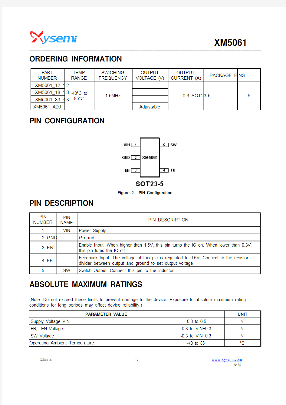
PIN CONFIGURATION
Figure 2. PIN Configuration
PIN DESCRIPTION
PIN
NUMBER
PIN NAME PIN DESCRIPTION
1
VIN
Power Supply
2 GND Ground.
3 EN
Enable Input. When higher than 1.5V, this pin turns the IC on. When lower than 0.3V, this pin turns the IC off. 4 FB
Feedback Input. The voltage at this pin is regulated to 0.6V. Connect to the resistor
divider between output and ground to set output voltage 5
SW
Switch Output. Connect this pin to the inductor.
ABSOLUTE MAXIMUM RATINGS
(Note: Do not exceed these limits to prevent damage to the device. Exposure to absolute maximum rating conditions for long periods may affect device reliability.) PARAMETER VALUE UNIT
Supply Voltage VIN -0.3 to 6.5 V FB, EN Voltage
-0.3 to VIN+0.3 V SW Voltage
-0.3 to VIN+0.3 V Operating Ambient Temperature
-40 to 85
°C
XM5061
____________________________________________________________________________________________________________________________
XySemi Inc - 3 - https://www.doczj.com/doc/f57029610.html,
Maximum Junction Temperature 125 °C Storage Temperature
-55 to 150 °C Lead Temperature (Soldering, 10 sec)
300
°C
ELECTRICAL CHARACTERISTICS
(V IN = 3.6V, T A = 25°C unless otherwise specified)
PARAMETER SYMBOL
TEST CONDITIONS
MIN TYP MAX UNIT
Input Voltage Range V IN
2.0 6.0 V UVLO Threshold V UVLO
V HYSTERESIS =100mV
1.0 1.4 1.8 V Operating Supply Current
V FB =0.5V or V OUT =90%, I Load =0
130 170
Shutdown Supply Current
I SUPPLY
V EN =0V, V IN =4.2V
0.1
1
μA T a =25°C
0.588 0.6 0.6120< T a <85°C 0.5865 0.6 0.6135Regulated Feedback Voltage
V FB
-40°C < T a <85°C
0.585 0.6 0.615V
Reference Voltage Line
Regulation
V IN =2.7V to 5.5V
0.04
0.4
% Regulated Output Voltage V OUT V OUT =1.8V; I OUT =100mA
1.746 1.8 1.854
V Output Voltage Load Regulation
0.5 % Peak Inductor Current
I PEAK
V IN =3V, V FB =0.5V or V OUT =90%,Duty Cycle<35%
1 A V FB =0.6V or V OUT =
100% 1.2 1.5 1.8 MHz Oscillator Frequency F OSC
V FB =0 or V OUT =0
220 KHz Rds(ON) of P-channel FET I SW =100mA 0.3 0.4 Ohm Rds(ON) of N-channel FET I SW =-100mA 0.2 0.3 Ohm Enable Threshold V IN = 2.5V to 5.5V 0.3 1 1.5 V Enable Leakage Current
-0.1 0.1
μA
SW Leakage Current
V EN = 0V, V SW = 0V or 5V, V IN = 5V
-1
1 uA
XM5061
____________________________________________________________________________________________________________________________
XySemi Inc - 4 - https://www.doczj.com/doc/f57029610.html,
Figure 3. Functional Block Diagram
FUNCTIONAL DESCRIPTION
NORMAL OPERATION
In normal operation the high-side MOSFET turns on each cycle and remains on until the current comparator turns it off. At this point the low-side MOSFET turns on and remains on until either the end of the switching cycle or until the inductor current approaches zero. The error amplifier adjusts the current comparator’s threshold as necessary in order to ensure that the output remains in regulation.
OVER CURRENT OPERATION
The part has internal current limit function, which is detected cycle by cycle. When its maximum inductor current limit is reached the charging cycle is terminated, and the low-side MOSFET is turned on to allow the inductor current to decrease. Under extreme overloads, such as short-circuit conditions, it reduces the oscillator frequency to 220KHz to allow further inductor current reduction and to minimize power dissipation.
APPLICATION INFORMATION
INDUCTOR SELECTION
In normal operation, the inductor maintains continuous current to the output. The inductor current has a ripple that is dependent on the inductance value. The high inductance reduces the ripple current. In general, select the inductance by the following equation:
()
×?=
??V OUT IN OUT IN V V V L V f I
Where OUT V is the output voltage, IN V is the input voltage, f is the switch frequency, and V I is the peak-to-peak inductor ripple current. Typically, choose V I as the 30% of the maximum output current.
XM5061
____________________________________________________________________________________________________________________________
XySemi Inc - 5 - https://www.doczj.com/doc/f57029610.html, Manufa cturer Part Number Induct ance(u H) DRC max (Ohms
) Dimensions L*W*H(mm3)
1 0.06 2.
2 0.09 Murata LQH32P
N
4.7 0.15
3.2*2.5*1.7 1.5 0.04 2.2 0.07 3.3 0.11 Sumida CDRH3D
16
4.7 0.16
4*4*1.8 Table 1. Recommend Surface Mount Inductors
INPUT CAPACITOR SELECTION
The input capacitor reduces input voltage ripple to the converter, low ESR ceramic capacitor is highly recommended. For most applications, a 4.7uF capacitor is used. The input capacitor should be placed as close as possible to VIN and GND.
OUTPUT CAPACITOR SELECTION
A low ESR output capacitor is required in order to maintain low output voltage ripple. In the case of ceramic output capacitors, capacitor ESR is very small and does not contribute to the ripple, so a lower capacitance value is acceptable when ceramic capacitors are used. A 10uF ceramic output capacitor is suitable for most applications.
OUTPUT VOLTAGE PROGRAMMING
In the adjustable version, the output voltage is set by a resistive divider according to the following equation:
??
=×?????
2110.6OUT V R R
Typically choose R1=100K and determine R2 from
the following equation:
Connect a small capacitor across R1 feed forward capacitance at the FB pin for better performance.
Figure 4. Typical Application Circuit for Adjustable Version
XM5061
____________________________________________________________________________________________________________________________
XySemi Inc - 6 - https://www.doczj.com/doc/f57029610.html, TYPICAL PERFORMANCE CHARACTERISTICS
(VIN=VEN=3.6V, L=2.2uH, CIN=4.7uF, COUT=10uF ,if not mentioned)
Efficiency vs. Output Current(VIN=5V)
Oscillator Frequency vs. Temperature
Reference Voltage vs. Temperature
DC Regulation(Vout=1.8V)
DC Regulation(Vout=3.3V)
Line Regulation (Vout=1.8V)
XM5061
____________________________________________________________________________________________________________________________
XySemi Inc - 7 - https://www.doczj.com/doc/f57029610.html, Steady State Waveform
Iout=0mA
Vout=1.8V VOUT
10mV/DIV
10ms/DIV
Vin=3.6V Steady State Waveform
Iout=600mA
Vout=1.8V VOUT
10mV/DIV
400ns/DIV
SW
5V/DIV
IL
1A/DIV
Vin=3.6V Steady State Waveform
Iout=50mA
Vout=1.8V VOUT
10mV/DIV
400ns/DIV
SW
5V/DIV
IL
500mA/DIV
Vin=3.6V
Load Transient Waveform
Iout=0~600mA
Vout=1.8V
VOUT
100mV/DIV
100us/DIV
ILOAD
500mA/DIV
IL
500mA/DIV
Vin=3.6V
Load Transient Waveform
Iout=200-600mA
Vout=1.8V
VOUT
50mV/DIV
100us/DIV
ILOAD
500mA/DIV
IL
500mA/DIV
Vin=3.6V
Startup through Enable Waveform
Iout=600mA
Vout=1.8V VOUT
1V/DIV
40us/DIV
EN
5V/DIV
Vin=3.6V
XM5061
____________________________________________________________________________________________________________________________
XySemi Inc - 8 - https://www.doczj.com/doc/f57029610.html,
PACKAGE OUTLINE
SOT23-5 PACKAGE OUTLINE AND DIMENSION
DIMENSION
IN
MILIMETERS DIMENSION
IN INCHES
SYMB OL
MIN
MAX MIN MAX A 1.050 1.250 0.041 0.049A1 0.0000.100 0.000 0.004A2 1.050 1.150 0.041 0.045b 0.3000.400 0.012 0.016c 0.1000.200 0.004 0.008D 2.820 3.020 0.111 0.119E 1.500 1.700 0.059 0.067E1 2.650 2.950 0.104 0.116
e
0.950 TYP
0.037 TYP
e1 1.800
2.000 0.071 0.079L 0.700 REF 0.028 REF L1 0.300
0.600 0.012 0.024
θ 0° 8° 0° 8°