
ChipScope Debug Lab
Introduction
This lab guides you through the process of inserting ChipScope-Pro cores into your design and performing on-chip verification.
Objectives
After completing this lab, you will be able to:
? Create a new ChipScope-Pro source in ISE
? Create ILA and ICON cores using ChipScope-Pro and insert it into a PicoBlaze design ? Specify trigger options in ChipScope Analyzer
? Download the bitstream and run the design in hardware
? Perform an on-chip verification and view the wave forms in ChipScope Analyzer
Design Description
You will extend the lab 5 design by adding a ChipScope ILA core to the PicoBlaze output bus. Next, you will setup the trigger to capture data when text is entered via Hyper Terminal. You should see the resulting text displayed in ChipScope when the buffer is full.
Procedure
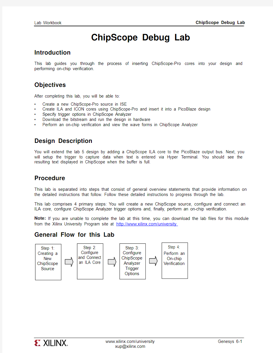
This lab is separated into steps that consist of general overview statements that provide information on the detailed instructions that follow. Follow these detailed instructions to progress through the lab. This lab comprises 4 primary steps: You will create a new ChipScope source, configure and connect an ILA core, configure ChipScope Analyzer trigger options and, finally, perform an on-chip verification. Note: If you are unable to complete the lab at this time, you can download the lab files for this module from the Xilinx University Program site at https://www.doczj.com/doc/f74192912.html,/university
General Flow for this Lab
Step 1:
Creating a New ChipScope Source
Step 2: Configure and Connect an ILA Core Step 3:
Configure ChipScope Analyzer Trigger Options
Step 4: Perform an On-chip Verification
Create a New ChipScope Source Step 1 1-1. Open a ChipScope-Pro project from lab6 folder (under vhdl or verilog).
1-1-1. Open the Xilinx ISE software by selecting Start All Programs Xilinx ISE Design Suite
13.2 ISE Design Tools Project Navigator.
1-1-2. Open the project by selecting File Open Project.
○Verilog users: Browse to c:\xup\fpgaflow\labs\verilog\lab6\chipccope
○VHDL users: Browse to c:\xup\fpgaflow\labs\vhdl\lab6\chipscope
1-1-3. Select chipscope.xise and click Open.
1-1-4. Create a new ChipScope Definition and Connection File source by selecting Project New Source and entering the name loopback_cs. Click Next to continue.
Figure 1. New Source Dialog Box
1-1-5. Click Finish. A ChipScope-Pro source will be added to the Sources in Project window.
Genesys 6-2 https://www.doczj.com/doc/f74192912.html,/university
Figure 2. ChipScope Definition and Connection (.cdc) added to VHDL Project
Configure and Connect an ILA Core Step 2 2-1. Connect the ILA core to the PicoBlaze output.
2-1-1. Double-click the loopback_cs.cdc file in the sources in project window to open the core inserter project.
Figure 3. ChipScope-Pro Core Inserter
Note: Projects saved in the Core Inserter hold all relevant information about source files, destination files, core parameters and core settings.
2-1-2. Click Next and then click New ILA Unit. Notice in the left hand window how an instance of the ILA core, U0:ILA, is added to the system.
Genesys 6-4 https://www.doczj.com/doc/f74192912.html,/university
Figure 4. Insert a new integrated logic analyzer (ILA) Unit
2-1-3. Click Next to setup the trigger parameters.
Each ILA or ILA/ATC core can have up to 16 separate trigger ports that can be setup independently. The individual trigger ports are buses that are made up of individual signals or bits that can range from 1 to 256 bits. Each trigger port can be connected to 1 to 16 match units. A match unit is a comparator that is connected to a trigger port and is used to detect events on that trigger port. The results of one or more match units are combined together to form the overall trigger condition event that is used to control the capturing of data. The different comparisons or match functions that can be performed by the trigger port match units depend on the type of match unit. The ILA and ILA/ITC cores support six types of match units. In this lab, you will setup the ILA core to trigger via some UART control signals.
2-1-4. Set the following ILA trigger parameters as follows and then click Next.
Trigger Input and Match Unit Settings.
? Number of input trigger ports: 3
Trigger Port Trigger Width # Match Units Counter Width
Match Type TRIG0 1 1 Disabled Basic TRIG1 1 1 Disabled Basic TRIG2
1
1
Disabled
Basic
Trigger Condition Settings
? Enable Trigger Sequencer: Checked (This allows you to specify a sequence of events to enable triggering)
?
Max Number of Sequencer Levels: 2
Storage Qualification Condition Settings
? Enable Storage Qualification: Checked (This allows you to specify which data will be stored in the internal buffer)
Figure 5. Specify the Trigger Parameters
The maximum number of data sample words that the ILA core can store in the sample buffer is called the data depth. The data depth determines the number of data width bits contributed by each block RAM unit used by the ILA unit. The maximum number of data sample words that can be captured depends on the number and size of block RAM, which varies according to device family and density.
2-1-5. Set the following capture parameters and click Next.
? Data Depth: 1024
? Sample On: Rising clock edge
? Data Same as Trigger Port: unchecked
? Data Width: 8
Figure 6. Specify Trigger Parameters
The net connections tab allows you to choose the signals to connect to the ILA core. If trigger is separate from data, then clock, trigger, and data must be specified. Connections that have not been made will appear in red.
Figure 7. Unconnected Net Connections
2-1-6. Click the Modify Connections tab.
Figure 8. Net Connections
The Select Net dialog provides an easy interface to choose nets to connect to the ILA, ILA/ATC or ATC2 cores. The hierarchical structure of the design can be traversed using the Structure/Nets pane. All the design’s nets of the selected structure hierarchy appear in the table at the lower left pane. The Clock Signals and Trigger/Data Signals tabs illustrate the net connections between the design and the ILA core.
2-1-7. With the Clock Signals tab under Net Selections selected, highlight the entry for clk55MHz in the listing of nets and click the Make Connections button to connect the clock signal in the design to the clock port of the ILA core.
Figure 9. Connect the clock
Genesys 6-6 https://www.doczj.com/doc/f74192912.html,/university
2-1-8. Click the Trigger Signals tab, and connect the three trigger ports as follows:
? TP0: data_present (this signal indicates that data is present in the uart_rx module
? TP1: read_from_uart (input to uart_rx that indicates that a read operation will occur)
? TP2: write_to_uart (input to uart_tx that indicates that a write operation will occur)
2-1-9. Click the Data Signals tab and connect the output port of the PicoBlaze controller to the data port of the ILA core (see Figure 10), and click OK.
Figure 10. Connect the PicoBlaze output port
2-1-10. You will notice that the Clock, Trigger, and Data ports under Net Connections are highlighted in black, indicating valid connections. Click Return to Project Navigator and save the file.
Figure 11. Connection between Design and ILA core Established
Configure ChipScope Analyzer Trigger Options Step 3 3-1. You will download the bitstream using ChipScope and configure the ILA core to trigger when the UART reads text from Hyper Terminal.
3-1-1. With the top-level file (loopback.v/vhd) selected, double-click on Analyze Design Using ChipScope in the Processes window.
3-1-2. Connect up the download cable and power up the Genesys board.
3-1-3. Click the Open Cable/Search JTAG Chain button.
Figure 12. Establish JTAG Connection
3-1-4. Chipscope Pro Analyzer will automatically detect the devices on the Genesys board and then click OK.
Figure 13. Impact Detects Devices in JTAG Chain
3-1-5. Right Click on the xc5vlx50t device and select configure.
3-1-6. Click Select New File and select the loopback.bit bitstream file from the project directory. Note that the import cdc file field shows the cdc file located in the project directory. Also note that the tool will create a bus (out_port) automatically. Click OK.
Double-click on Trigger Setup and Waveform entries in Project Tree to open the respective windows.
The ChipScope Pro Analyzer interface consists of four parts:
Genesys 6-8 https://www.doczj.com/doc/f74192912.html,/university
Figure 14. ChipScope Analyzer Window
Each ChipScope Pro ILA, ILA/ATC, and IBA core has its own Trigger setup window, which provides a graphical interface for the user to setup triggers. The trigger mechanism inside each ChipScope Pro core can be modified at run-time without having to recompile the design. There are three components to the trigger mechanism:
? Match Functions: Defines the match or comparison value of each match unit
? Trigger Conditions: Defines the overall trigger condition based on a binary equation or sequence of one or more match functions
? Capture Settings: Defines how many samples to capture, how many capture windows, and the position of the trigger in those windows
In this design, you will setup the triggers to capture text at the PicoBlaze output port, after being entered via Hyper Terminal.
3-1-7. Specify the Match Units as follows:
? M0:TriggerPort0 (data_present): Value 1
? M1:TriggerPort1(read_from_uart): Value 1
? M2:TriggerPort1(write_to_uart): Value 1
Figure 15. Setup the Match Units
3-1-8. Click the field under Trigger Condition Equation, set the equation M0 M1 in the Sequencer
tab, and then click OK.
Genesys 6-10 https://www.doczj.com/doc/f74192912.html,/university
Figure 16. Trigger Condition Equation
3-1-9. Check the field next to Storage Qualification , select the AND Equation , and check M2. Click
OK . This will enable the ILA core to capture data in the buffer only when data is present, and not on every single clock edge.
Figure 17. Storage Qualification Equation
Perform an On-Chip Verification
Step 4
4-1.
Start Hyper-Terminal program. Set baud rate to 9600. Arm the trigger and view the waveforms of the captured data.
4-1-1.
Start the Hyper-Terminal program. Make sure that the baud rate is set to 9600.
4-1-2. Set the buffer depth to 16.
Figure 18. Select Buffer Depth
4-1-3. Cick the Apply Settings and Arm Trigger button.
Figure 19. Apply Settings and Arm Trigger
4-1-4. Type “Xilinx #1 FPGA!” in Hyper Terminal and view the message in ChipScope Analyzer.
Figure 20. Output in Waveform Window
4-1-5. Close all applications without saving ChipScope project.
Conclusion
You inserted the ILA and ICON cores into the PicoBlaze design, set up trigger conditions in ChipScope Analyzer, performed an on-chip verification, and analyzed the waveforms in ChipScope-Pro Analyzer.