192 kHz Digital Audio Interface Receiver
Features
Complete EIAJ CP1201, IEC-60958, AES3, S/PDIF-Compatible Receiver
+3.3V Analog Supply (VA)
+3.3V Digital Supply (VD)
+3.3V or +5.0V Digital Interface Supply (VL) 8:2 S/PDIF Input MUX
AES/SPDIF Input Pins Selectable in Hardware Mode
Three General Purpose Outputs (GPO) Allow Signal Routing
Selectable Signal Routing to GPO Pins
S/PDIF-to-TX Inputs Selectable in Hardware Mode
Flexible 3-wire Serial Digital Output Port 32kHz to 192kHz Sample Frequency Range Low-Jitter Clock Recovery
Pin and Microcontroller Read Access to Channel Status and User Data
SPI? or I2C? Control Port Software Mode and Stand-Alone Hardware Mode
Differential Cable Receiver
On-Chip Channel Status Data Buffer Memories Auto-Detection of Compressed Audio Input Streams
Decodes CD Q Sub-Code
OMCK System Clock Mode
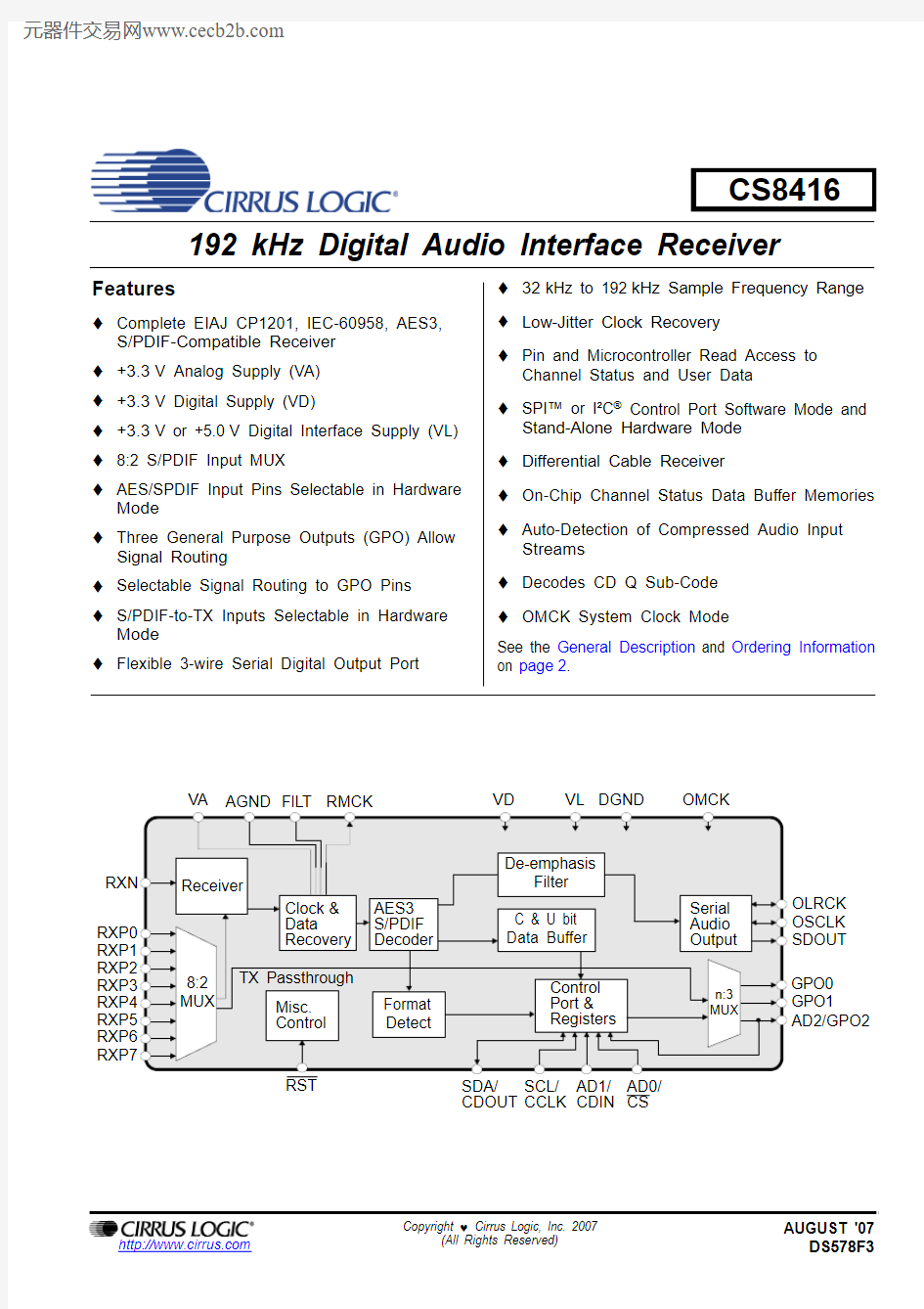
See the General Description and Ordering Information on page2.
CS8416
CS8416 General Description
The CS8416 is a monolithic CMOS device that receives and decodes one of eight stereo pairs of digital audio data according to the IEC60958, S/PDIF, EIAJ CP1201, or AES3 interface standards. The CS8416 has a serial digital audio output port and comprehensive control ability through a selectable control port in Software Mode or through selectable pins in Hardware Mode. Channel status data are assembled in buffers, making read access easy. GPO pins may be assigned to route a variety of signals to output pins.
A low-jitter clock recovery mechanism yields a very clean recovered clock from the incoming AES3 stream.
Stand-alone operation allows systems with no microcontroller to operate the CS8416 with dedicated output pins for channel status data.
The CS8416 is available in 28-pin TSSOP, SOIC, and QFN packages in Commercial grade (-10° to +70°C) and Automotive grade (-40° to +85°C). The CDB8416 Customer Demonstration board is also available for device eval-uation and implementation suggestions. Please refer to “Ordering Information” on page59 for complete ordering information.
Target applications include A/V receivers, CD-R, DVD receivers, multimedia speakers, digital mixing consoles, ef-fects processors, set-top boxes, and computer and automotive audio systems.
CS8416 TABLE OF CONTENTS
1. CHARACTERISTICS AND SPECIFICATIONS (6)
SPECIFIED OPERATING CONDITIONS (6)
ABSOLUTE MAXIMUM RATINGS (6)
DC ELECTRICAL CHARACTERISTICS (7)
DIGITAL INPUT CHARACTERISTICS (7)
DIGITAL INTERFACE SPECIFICATIONS (7)
SWITCHING CHARACTERISTICS (8)
SWITCHING CHARACTERISTICS - SERIAL AUDIO PORTS (9)
SWITCHING CHARACTERISTICS - CONTROL PORT - SPI MODE (10)
SWITCHING CHARACTERISTICS - CONTROL PORT- I2C FORMAT (11)
2. PIN DESCRIPTION - SOFTWARE MODE (12)
2.1 TSSOP Pin Description (12)
2.2 QFN Pin Description (14)
3. PIN DESCRIPTION - HARDWARE MODE (16)
3.1 TSSOP Pin Description (16)
3.2 QFN Pin Description (18)
4. TYPICAL CONNECTION DIAGRAMS (20)
5. APPLICATIONS (22)
5.1 Reset, Power-Down and Start-Up (22)
5.2 ID Code and Revision Code (22)
5.3 Power Supply, Grounding, and PCB Layout (22)
6. GENERAL DESCRIPTION (23)
6.1 AES3 and S/PDIF Standards Documents (23)
7. SERIAL AUDIO OUTPUT PORT (23)
7.1 Slip/Repeat Behavior (25)
7.2 AES11 Behavior (26)
8. S/PDIF RECEIVER (27)
8.1 8:2 S/PDIF Input Multiplexer (27)
8.1.1 General (27)
8.1.2 Software Mode (27)
8.1.3 Hardware Mode (28)
8.2 OMCK System Clock Mode (28)
8.3 Clock Recovery and PLL Filter (28)
9. GENERAL PURPOSE OUTPUTS (29)
10. ERROR AND STATUS REPORTING (30)
10.1 General (30)
10.1.1 Software Mode (30)
10.1.2 Hardware Mode (30)
10.2 Non-Audio Detection (31)
10.2.1 Format Detection (31)
10.3 Interrupts (31)
11. CHANNEL STATUS AND USER-DATA HANDLING (32)
11.1 Software Mode (32)
11.2 Hardware Mode (32)
12. CONTROL PORT DESCRIPTION (33)
12.1 SPI Mode (33)
12.2 I2C Mode (34)
13. CONTROL PORT REGISTER QUICK REFERENCE (35)
14. CONTROL PORT REGISTER DESCRIPTIONS (36)
14.1 Memory Address Pointer (MAP) (36)
14.2 Control0 (00h) (36)
14.3 Control1 (01h) (37)
CS8416
14.4 Control2 (02h) (38)
14.5 Control3 (03h) (39)
14.6 Control4 (04h) (39)
14.7 Serial Audio Data Format (05h) (40)
14.8 Receiver Error Mask (06h) (41)
14.9 Interrupt Mask (07h) (41)
14.10 Interrupt Mode MSB (08h) and Interrupt Mode LSB(09h) (41)
14.11 Receiver Channel Status (0Ah) (42)
14.12 Format Detect Status (0Bh) (42)
14.13 Receiver Error (0Ch) (43)
14.14 Interrupt 1 Status (0Dh) (44)
14.15 Q-Channel Subcode (0Eh - 17h) (44)
14.16 OMCK/RMCK Ratio (18h) (45)
14.17 Channel Status Registers (19h - 22h) (45)
14.18 IEC61937 PC/PD Burst Preamble (23h - 26h) (45)
14.19 CS8416 I.D. and Version Register (7Fh) (45)
15. HARDWARE MODE (46)
15.1 Serial Audio Port Formats (46)
15.2 Hardware Mode Function Selection (46)
15.3 Hardware Mode Equivalent Register Settings (47)
16. EXTERNAL AES3/SPDIF/IEC60958 RECEIVER COMPONENTS (49)
16.1 AES3 Receiver External Components (49)
16.2 Isolating Transformer Requirements (49)
17. CHANNEL STATUS BUFFER MANAGEMENT (51)
17.1 AES3 Channel Status (C) Bit Management (51)
17.2 Accessing the E Buffer (51)
17.2.1 Serial Copy Management System (SCMS) (51)
18. PLL FILTER (53)
18.1 General (53)
18.2 External Filter Components (53)
18.2.1 General (53)
18.2.2 Capacitor Selection (54)
18.2.3 Circuit Board Layout (54)
18.2.4 Component Value Selection (54)
18.2.5 Jitter Attenuation (55)
19. PACKAGE DIMENSIONS (56)
TSSOP THERMAL CHARACTERISTICS (57)
QFN THERMAL CHARACTERISTICS (58)
20. ORDERING INFORMATION (59)
21. REVISION HISTORY (60)
CS8416 LIST OF FIGURES
Figure 1. Audio Port Master Mode Timing (9)
Figure 2. Audio Port Slave Mode and Data Input Timing (9)
Figure 3. SPI Mode Timing (10)
Figure 4. I2C Mode Timing (11)
Figure 5. Typical Connection Diagram - Software Mode (20)
Figure 6. Typical Connection Diagram - Hardware Mode (21)
Figure 7. Serial Audio Output Example Formats (24)
Figure 8. AES3 Data Format (25)
Figure 9. Receiver Input Structure (27)
Figure 10. C/U Data Outputs (32)
Figure 11. Control Port Timing in SPI Mode (33)
Figure 12. Control Port Timing, I2C Slave Mode Write (34)
Figure 13. Control Port Timing, I2C Slave Mode Read (34)
Figure 14. De-Emphasis Filter Response (39)
Figure 15. Hardware Mode Data Flow (46)
Figure 16. Professional Input Circuit (49)
Figure 17. Transformerless Professional Input Circuit (49)
Figure 18. Consumer Input Circuit (50)
Figure 19. S/PDIF MUX Input Circuit (50)
Figure 20. TTL/CMOS Input Circuit (50)
Figure 21. Channel Status Data Buffer Structure (52)
Figure 22. Flowchart for Reading the E Buffer (52)
Figure 23. PLL Block Diagram (53)
Figure 24. Recommended Layout Example (54)
Figure 25. Jitter Attenuation Characteristics of PLL (55)
LIST OF TABLES
Table 1. Typical Delays by Frequency Values (26)
Table 2. Clock Switching Output Clock Rates (28)
Table 3. GPO Pin Configurations (29)
Table 4. Hardware Mode Start-Up Pin Conditions (47)
Table 5. Hardware Mode Serial Audio Format Select (48)
Table 6. External PLL Component Values (54)
CS8416
1.CHARACTERISTICS AND SPECIFICATIONS
All Min/Max characteristics and specifications are guaranteed over the Specified Operating Conditions. Typical performance characteristics and specifications are derived from measurements taken at nominal supply voltages and T A = 25°C.
SPECIFIED OPERATING CONDITIONS
(AGND, DGND = 0V, all voltages with respect to 0V)
ABSOLUTE MAXIMUM RATINGS
(AGND, DGND = 0V; all voltages with respect to 0V. Operation beyond these limits may result in permanent dam-age to the device. Normal operation is not guaranteed at these extremes.)
Notes:
1.Transient currents of up to 100mA will not cause SCR latch-up.
Parameter
Symbol Min Typ
Max
Units
Power Supply Voltage
VA VD VL 3.133.133.13 3.33.33.3 or 5.0
3.463.465.25V V V Ambient Operating Temperature:
Commercial Grade Automotive Grade
T A
-10-40
--
+70+85
°C
Parameter
Symbol
Min
Max
Units
Power Supply Voltage
VA, VD,VL
- 6.0V Input Current, Any Pin Except Supplies (Note 1)
I in -±10mA Input Voltage
V in -0.3(VL) + 0.3V Ambient Operating Temperature (power applied)T A -55125°C Storage Temperature
T stg
-65150°C
CS8416
DC ELECTRICAL CHARACTERISTICS
(AGND = DGND = 0V; all voltages with respect to 0V.)
Notes:
2.Power-Down Mode is defined as RST = LO with all clocks and data lines held static.
3.Normal operation is defined as RST = HI.
4.Assumes that no inputs are floating. It is recommended that all inputs be driven high or low at all times.
DIGITAL INPUT CHARACTERISTICS
(AGND = DGND = 0V; all voltages with respect to 0V.)
DIGITAL INTERFACE SPECIFICATIONS
(AGND = DGND = 0V; all voltages with respect to 0V.)
Parameters
Symbol
Min
Typ
Max
Units Power-Down Mode (Notes 2, 4)
Supply Current in power-down
VA VD
VL = 3.3V VL = 5.0V IA ID IL IL ----10701012----μA μA μA μA
Normal Operation (Notes 3, 4)
Supply Current at 48kHz frame rate
VA VD
VL = 3.3V VL = 5.0V
IA ID IL IL ---- 5.75.92.84.2----mA mA mA mA Supply Current at 192kHz frame rate
VA VD
VL = 3.3V VL = 5.0V
IA ID IL IL
----
9.4237.811.8
----
mA mA mA mA
Parameters
Symbol Min Typ
Max
Units Input Leakage Current
I IN --±0.5μA
Differential Input Sensitivity, RXP[7:0] to RXN V TH -150200mVpp Input Hysteresis
V H
0.15- 1.0
V
Parameters
Symbol Min Max
Units
High-Level Output Voltage (I OH = -3.2mA)V OH (VL) - 1.0
-V Low-Level Output Voltage (I OL = 3.2mA)V OL -0.5V High-Level Input Voltage, except RXP[7:0], RXN V IH 2.0(VL) + 0.3
V Low-Level Input Voltage, except RXP[7:0], RXN
V IL
-0.3
0.8
V
CS8416
SWITCHING CHARACTERISTICS
(Inputs: Logic 0 = 0V, Logic 1 = VL; C L = 20pF)
Notes:
5.Typical RMS cycle-to-cycle jitter.
6.Duty cycle when clock is recovered from biphase encoded input.
7.Duty cycle when OMCK is switched over for output on RMCK.
Parameter
Symbol
Min
Typ
Max
Units RST Pin Low Pulse Width
200--μS
PLL Clock Recovery Sample Rate Range 30-200kHz RMCK Output Jitter (Note 5)-200-ps
RMS RMCK Output Duty-Cycle
(Note 6)(Note 7)
455050555565%%RMCK/OMCK Maximum Frequency
-
-
50
MHz
CS8416
SWITCHING CHARACTERISTICS - SERIAL AUDIO PORTS
(Inputs: Logic 0 = 0V, Logic 1 = VL; C L = 20pF)
Notes:
8.In Software Mode the active edges of OSCLK are programmable.9.In Software Mode the polarity of OLRCK is programmable.
10.This delay is to prevent the previous OSCLK edge from being interpreted as the first one after OLRCK
has changed.11.This setup time ensures that this OSCLK edge is interpreted as the first one after OLRCK has changed.
Parameter
Symbol
Min
Typ
Max
Units
OSCLK/OLRCK Active Edge to SDOUT Output Valid (Note 8)t dpd --23ns Master Mode
RMCK to OSCLK active edge delay (Note 8)t smd 0-12ns RMCK to OLRCK delay (Note 9)t lmd
0-12ns OSCLK and OLRCK Duty Cycle -50-%Slave Mode OSCLK Period
t sckw 36--ns OSCLK Input Low Width t sckl 14--ns OSCLK Input High Width
t
sckh 14--ns OSCLK Active Edge to OLRCK Edge (Notes 8,9,10)t lrckd 10--ns OSCLK Edge Setup Before OSCLK Active-Edge (Notes 8,9,11)
t lrcks
10
-
-
ns
Figure 1. Audio Port Master Mode Timing Figure 2. Audio Port Slave Mode and Data Input
CS8416
SWITCHING CHARACTERISTICS - CONTROL PORT - SPI MODE
(Inputs: Logic 0 = 0V, Logic 1 = VL; C L = 20pF)
Notes:
12.If Fs is lower than 46.875kHz, the maximum CCLK frequency should be less than 128Fs. This is dic-tated by the timing requirements necessary to access the Channel Status memory. Access to the con-trol register file can be carried out at the full 6MHz rate. The minimum allowable input sample rate is 32kHz, so choosing CCLK to be less than or equal to 4.1MHz should be safe for all possible conditions.13.Data must be held for sufficient time to bridge the transition time of CCLK.14.For f sck <1MHz.
Parameter
Symbol
Min
Max
Unit
CCLK Clock Frequency
(Note 12)
f sck 0 6.0MHz CS High Time Between Transmissions t csh 1.0-μs CS Fallin
g to CCLK Edge t css 20-ns CCLK Low Time t scl 66-ns CCLK Hig
h Time
t sch 66-ns CDIN to CCLK Rising Setup Time t dsu 40-ns CCLK Rising to DATA Hold Time (Note 13)
t dh 15-ns CCLK Falling to CDOUT Stable t pd -50ns Rise Time of CDOUT t r1-25ns Fall Time of CDOUT
t f1-25ns Rise Time of CCLK and CDIN (Note 14)t r2-100ns Fall Time of CCLK and CDIN
(Note 14)
t r2
-
100
ns
Figure 3. SPI Mode Timing
CS8416
SWITCHING CHARACTERISTICS - CONTROL PORT- I2C FORMAT
(Inputs: Logic 0 = 0V, Logic 1 = VL; C L = 20pF)
Notes:
15.Data must be held for sufficient time to bridge the 300ns transition time of SCL.
Parameter
Symbol
Min
Max
Unit
SCL Clock Frequency
f scl -100kHz Bus Free Time Between Transmissions
t buf 4.7-μs Start Condition Hold Time (prior to first clock pulse)t hdst 4.0-μs Clock Low time t low 4.7-μs Clock High Time
t high 4.0-μs Setup Time for Repeated Start Condition t sust 4.7-μs SDA Hold Time from SCL Falling (Note 15)t hdd 10-ns SDA Setup time to SCL Rising t sud 250-ns Rise Time of SCL and SDA t r -1000ns Fall Time SCL and SDA
t f -300ns Setup Time for Stop Condition
t susp
4.7-μs
Figure 4. I2C Mode Timing
CS8416 2.PIN DESCRIPTION - SOFTWARE MODE
2.1TSSOP Pin Description
Pin
Name
Pin #Pin Description
VA6Analog Power (Input) - Analog power supply. Nominally +3.3V. This supply should have as little noise as possible since noise on this pin will directly affect the jitter performance of the recovered clock
VD23Digital Power (Input) – Digital core power supply. Nominally +3.3V
VL21Logic Power (Input) – Input/Output power supply. Nominally +3.3V or +5.0V
AGND7Analog Ground (Input) - Ground for the analog circuitry in the chip. AGND and DGND should be con-nected to a common ground area under the chip.
DGND22Digital & I/O Ground (Input) - Ground for the I/O and core logic. AGND and DGND should be connected to a common ground area under the chip.
RST9Reset (Input) - When RST is low, the CS8416 enters a low power mode and all internal states are reset. On initial power up, RST must be held low until the power supply is stable, and all input clocks are stable in frequency and phase.
FILT8PLL Loop Filter (Output) - An RC network should be connected between this pin and analog ground. For minimum PLL jitter, return the ground end of the filter network directly to AGND. See “PLL Filter” on page53 for more information on the PLL and the external components.
RXP0 RXP1 RXP2 RXP3 RXP4 RXP5 RXP6 RXP7
4
3
2
1
10
11
12
13
Positive AES3/SPDIF Input (Input) - Single-ended or differential receiver inputs carrying AES3 or
S/PDIF encoded digital data. The RXP[7:0] inputs comprise the 8:2 S/PDIF Input Multiplexer. The select line control is accessed using the Control 4 register (04h). Unused multiplexer inputs should be left float-ing or tied to AGND. See “External AES3/SPDIF/IEC60958 Receiver Components” on page49 for rec-ommended input circuits.
RXP3OLRCK
RXP2OSCLK
RXP1SDOUT
RXP0OMCK
RXN RMCK
VA VD
AGND DGND
FILT VL
RST GPO0
RXP4GPO1
RXP5AD2 / GPO2
RXP6SDA / CDOUT
RXP7SCL / CCLK
AD0 / CS AD1 / CDIN
CS8416
RXN
5
Negative AES3/SPDIF Input (Input ) - Single-ended or differential receiver input carrying AES3 or S/PDIF encoded digital data. Used along with RXP[7:0] to form an AES3 differential input. In single-ended operation this should be AC coupled to ground through a capacitor. See “External AES3/SPDIF/IEC60958 Receiver Components” on page 49 for recommended input circuits.
OMCK 25
System Clock (Input ) - When the OMCK System Clock Mode is enabled using the SWCLK bit in the Control 1 register, the clock signal input on this pin is automatically output through RMCK on PLL unlock. OMCK serves as the reference signal for OMCK/RMCK ratio expressed in register 18h. “OMCK System Clock Mode” section on page 28
RMCK 24Input Section Recovered Master Clock (Output ) - Input section recovered master clock output from the PLL. Frequency defaults to 256x the sample rate (F s ) and may be set to 128x through the RMCKF bit in the Control 1 register (01h). RMCK may also be set to high impedance by the RXD bit in the Control 4 register (04h).
OSCLK 27Serial Audio Output Bit Clock (Input /Output ) - Serial bit clock for audio data on the SDOUT pin OLRCK 28Serial Audio Output Left/Right Clock (Input /Output ) - Word rate clock for the audio data on the SDOUT pin. Frequency will be the output sample rate (Fs)
SDOUT 26
Serial Audio Output Data (Output ) - Audio data serial output pin. This pin must be pulled high to VL through a 47 k Ω resistor to place the part in Software Mode.
SDA / CDOUT 17
Serial Control Data I/O (I2C) / Data Out (SPI) (Input/Output ) - In I2C Mode, SDA is the control I/O data line. SDA is open drain and requires an external pull-up resistor to VL. In SPI Mode, CDOUT is the out-put data from the control port interface on the CS8416. See the “Control Port Description” section on page 33.
SCL / CCLK
16
Control Port Clock (Input ) - Serial control interface clock and is used to clock control data bits into and out of the CS8416. CCLK is an open drain output and requires an external pull-up resistor to VL. See the “Control Port Description” section on page 33.
AD0 / CS 14
Address Bit 0 (I2C) / Control Port Chip Select (SPI) (Input) - A falling edge on this pin puts the CS8416 into SPI Control Port Mode. With no falling edge, the CS8416 defaults to I2C Mode. In I2C Mode, AD0 is a chip address pin. In SPI Mode, CS is used to enable the control port interface on the CS8416. See the “Control Port Description” section on page 33.
AD1 / CDIN 15
Address Bit 1 (I2C) / Serial Control Data in (SPI) (Input ) - In I2C Mode, AD1 is a chip address pin. In SPI Mode, CDIN is the input data line for the control port interface. See the “Control Port Description” section on page 33.
AD2 / GPO218General Purpose Output 2 (Output) - If using the I2C control port, this pin must be pulled high or low through a 47k Ω resistor. See the “Control Port Description” section on page 33 and “General Purpose Outputs” on page 29 for GPO functions.
GPO119General Purpose Output 1 (Output) - See “General Purpose Outputs” on page 29 for GPO functions.GPO0
20
General Purpose Output 0 (Output) - See “General Purpose Outputs” on page 29 for GPO functions.
Pin Name
Pin #Pin Description
CS8416 2.2QFN Pin Description
Pin
Name
Pin #Pin Description
VA3Analog Power (Input) - Analog power supply. Nominally +3.3V. This supply should have as little noise as possible since noise on this pin will directly affect the jitter performance of the recovered clock
VD20Digital Power (Input) – Digital core power supply. Nominally +3.3V
VL18Logic Power (Input) – Input/Output power supply. Nominally +3.3V or +5.0V
AGND4Analog Ground (Input) - Ground for the analog circuitry in the chip. AGND and DGND should be con-nected to a common ground area under the chip.
DGND19Digital & I/O Ground (Input) - Ground for the I/O and core logic. AGND and DGND should be connected to a common ground area under the chip.
RST6Reset (Input) - When RST is low, the CS8416 enters a low power mode and all internal states are reset. On initial power up, RST must be held low until the power supply is stable, and all input clocks are stable in frequency and phase.
FILT5PLL Loop Filter (Output) - An RC network should be connected between this pin and analog ground. For minimum PLL jitter, return the ground end of the filter network directly to AGND. See “PLL Filter” on page53
for more information on the PLL and the external components.
R
X
P
1
R
X
P
2
R
X
P
3
O
L
R
C
K
O
S
C
L
K
S
D
O
U
T
O
M
C
K
R
X
P
5
R
X
P
6
R
X
P
7
A
D
/
C
S
A
D
1
/
C
D
I
N
S
C
L
/
C
C
L
K
S
D
A
/
C
D
O
U
T
RXP0
RXN
VA
AGND
FILT
RST
RXP4
RMCK
VD
DGND
VL
GPO0
GPO1
AD2 / GPO2
CS8416
RXP0RXP1RXP2RXP3RXP4RXP5RXP6RXP7128272678910Positive AES3/SPDIF Input (Input ) - Single-ended or differential receiver inputs carrying AES3 or
S/PDIF encoded digital data. The RXP[7:0] inputs comprise the 8:2 S/PDIF Input Multiplexer. The select line control is accessed using the Control 4 register (04h). Unused multiplexer inputs should be left float-ing or tied to AGND. See “External AES3/SPDIF/IEC60958 Receiver Components” on page 49 for rec-ommended input circuits.
RXN
2
Negative AES3/SPDIF Input (Input ) - Single-ended or differential receiver input carrying AES3 or S/PDIF encoded digital data. Used along with RXP[7:0] to form an AES3 differential input. In single-ended operation this should be AC coupled to ground through a capacitor. See “External AES3/SPDIF/IEC60958 Receiver Components” on page 49 for recommended input circuits.
OMCK 22
System Clock (Input ) - When the OMCK System Clock Mode is enabled using the SWCLK bit in the Control 1 register, the clock signal input on this pin is automatically output through RMCK on PLL unlock. OMCK serves as the reference signal for OMCK/RMCK ratio expressed in register 18h. “OMCK System Clock Mode” section on page 28
RMCK 21Input Section Recovered Master Clock (Output ) - Input section recovered master clock output from the PLL. Frequency defaults to 256x the sample rate (F s ) and may be set to 128x through the RMCKF bit in the Control 1 register (01h). RMCK may also be set to high impedance by the RXD bit in the Control 4 register (04h).
OSCLK 24Serial Audio Output Bit Clock (Input /Output ) - Serial bit clock for audio data on the SDOUT pin OLRCK 25Serial Audio Output Left/Right Clock (Input /Output ) - Word rate clock for the audio data on the SDOUT pin. Frequency will be the output sample rate (Fs)
SDOUT 23
Serial Audio Output Data (Output ) - Audio data serial output pin. This pin must be pulled high to VL through a 47 k Ω resistor to place the part in Software Mode.
SDA / CDOUT 14
Serial Control Data I/O (I2C) / Data Out (SPI) (Input/Output ) - In I2C Mode, SDA is the control I/O data line. SDA is open drain and requires an external pull-up resistor to VL. In SPI Mode, CDOUT is the out-put data from the control port interface on the CS8416. See the “Control Port Description” section on page 33.
SCL / CCLK
13
Control Port Clock (Input ) - Serial control interface clock and is used to clock control data bits into and out of the CS8416. CCLK is an open drain output and requires an external pull-up resistor to VL. See the “Control Port Description” section on page 33.
AD0 / CS 11
Address Bit 0 (I2C) / Control Port Chip Select (SPI) (Input) - A falling edge on this pin puts the CS8416 into SPI Control Port Mode. With no falling edge, the CS8416 defaults to I2C Mode. In I2C Mode, AD0 is a chip address pin. In SPI Mode, CS is used to enable the control port interface on the CS8416. See the “Control Port Description” section on page 33.
AD1 / CDIN 12
Address Bit 1 (I2C) / Serial Control Data in (SPI) (Input ) - In I2C Mode, AD1 is a chip address pin. In SPI Mode, CDIN is the input data line for the control port interface. See the “Control Port Description” section on page 33.
AD2 / GPO215General Purpose Output 2 (Output) - If using the I2C control port, this pin must be pulled high or low through a 47k Ω resistor. See the “Control Port Description” section on page 33 and “General Purpose Outputs” on page 29 for GPO functions.
GPO116General Purpose Output 1 (Output) - See “General Purpose Outputs” on page 29 for GPO functions.GPO017General Purpose Output 0 (Output) - See “General Purpose Outputs” on page 29 for GPO functions.THERMAL PAD
-
Thermal Pad - Thermal relief pad for optimized heat dissipation.
Pin Name
Pin #
Pin Description
CS8416 3.PIN DESCRIPTION - HARDWARE MODE
3.1TSSOP Pin Description
Pin Name Pin #Pin Description
VA6Analog Power (Input) - Analog power supply. Nominally +3.3V. This supply should have as little noise as possible since noise on this pin will directly affect the jitter performance of the recovered clock
VD23Digital Power (Input) – Digital core power supply. Nominally +3.3V
VL21Logic Power (Input) – Input/Output power supply. Nominally +3.3V or +5.0V
AGND7Analog Ground (Input) - Ground for the analog circuitry in the chip. AGND and DGND should be connected to a common ground area under the chip.
DGND22Digital & I/O Ground (Input) - Ground for the I/O and core logic. AGND and DGND should be con-nected to a common ground area under the chip.
RST9Reset (Input) - When RST is low, the CS8416 enters a low power mode and all internal states are reset. On initial power up, RST must be held low until the power supply is stable, and all input clocks are stable in frequency and phase.
FILT8PLL Loop Filter (Output) - An RC network should be connected between this pin and analog ground.
For minimum PLL jitter, return the ground end of the filter network directly to AGND. See “PLL Filter” on page53 for more information on the PLL and the external components.
RXP0 RXP1 RXP2 RXP34
3
2
1
Positive AES3/SPDIF Input (Input) - Single-ended or differential receiver inputs carrying AES3 or S/PDIF encoded digital data. The RXP[3:0] inputs comprise the 4:2 S/PDIF Input Multiplexer. The select line control is accessed using the RXPSEL[1:0] pins. Unused multiplexer inputs should be left floating or tied to AGND. See “External AES3/SPDIF/IEC60958 Receiver Components” on page49 for recommended input circuits.
RXN5Negative AES3/SPDIF Input (Input) - Single-ended or differential receiver input carrying AES3 or S/PDIF encoded digital data. Used along with RXP[3:0] to form an AES3 differential input. In single-ended operation this should be AC coupled to ground through a capacitor. See “External
AES3/SPDIF/IEC60958 Receiver Components” on page49 for recommended input circuits.
RXP3OLRCK
RXP2OSCLK
RXP1SDOUT
RXP0OMCK
RXN RMCK
VA VD
AGND DGND
FILT VL
RST TX
RXSEL1C
RXSEL0U
TXSEL1RCBL
TXSEL096KHZ
NV / RERR AUDIO
CS8416
OMCK
25
System Clock (Input ) - OMCK System Clock Mode is enabled by a transition (rising edge active) on OMCK after reset. When enabled, the clock signal input on this pin is automatically output through RMCK on PLL unlock. See “OMCK System Clock Mode” on page 28.
RMCK 24
Input Section Recovered Master Clock (Output ) - Input section recovered master clock output from the PLL. Frequency is 256x the sample rate (F s ) when the U pin is pulled down by a 47k Ω resistor to DGND. Frequency is 128x the sample rate (F s ) when the U pin is pulled up by a 47k Ω resistor to VL.
OSCLK 27Serial Audio Output Bit Clock (Input /Output ) - Serial bit clock for audio data on the SDOUT pin OLRCK 28Serial Audio Output Left/Right Clock (Input /Output ) - Word rate clock for the audio data on the SDOUT pin. Frequency will be the output sample rate (Fs)
SDOUT 26Serial Audio Output Data (Output ) - Audio data serial output pin. This pin must be pulled low to DGND through a 47k Ω resistor to place the part in Hardware Mode.
RXSEL1RXSEL01011Receiver MUX Selector (Input) - Used to select which pin, RXP[3:0], is used for the receiver input.TXSEL1TXSEL01213TX Pin MUX SELECTION (Input) - Used to select which pin, RXP[3:0], is passed to the TX pin out-put. If TX passthrough is not used, the user should set it to output one of the unused receiver inputs.TX
20
S/PDIF MUX Passthrough (Output) - Single-ended signal is resolved to full-rail, but is not de-jittered before it is output. Output is set by TXSEL[1:0]. This pin is also used to select the type of phase detector (PDUR) at reset. If TX passthrough is not used, the user should set it to output one of the unused receiver inputs.
NV/RERR 14Non-Validity Receiver Error/Receiver Error (Output) - Receiver error indicator. NVERR is selected by a 47k Ω resistor to DGND. RERR is selected by a 47k Ω resistor to VL.
AUDIO
15
Audio Channel Status Bit (Output) – When low, a valid linear PCM audio stream is indicated. See “Non-Audio Detection” on page 31. This pin is also used to select the serial port format (SFSEL1) at reset.
96KHZ 16
96kHz Sample Rate Detect (Output) - If the input sample rate is ≤ 48kHz, outputs a “0”. Outputs a “1” if the sample rate is ≥ 88.1kHz. Otherwise the output is indeterminate. Also used to set the Emphasis Audio Match feature at reset.
RCBL 17
Receiver Channel Status Block (Output) -Indicates the beginning of a received channel status block. RCBL goes high two frames after the reception of a Z preamble, remains high for 16 frames and then returns low for the remainder of the block. RCBL changes on rising edges of RMCK. Also used to set the serial audio port to master or slave at reset.
C 19Channel Status Data (Output ) - Outputs channel status data from the AES3 receiver, clocked by the rising and falling edges of OLRCK. Also used to select the serial port format (SFSEL0) at reset.U
18
User Data (Output ) - Outputs user data from the AES3 receiver, clocked by the rising and falling edges of OLRCK. Also used to select the frequency of RMCK to either 256*F s or 128*F s at reset.
Pin Name
Pin #
Pin Description
CS8416 3.2QFN Pin Description
Pin Name Pin #Pin Description
VA3Analog Power (Input) - Analog power supply. Nominally +3.3V. This supply should have as little noise as possible since noise on this pin will directly affect the jitter performance of the recovered clock
VD20Digital Power (Input) – Digital core power supply. Nominally +3.3V
VL18Logic Power (Input) – Input/Output power supply. Nominally +3.3V or +5.0V
AGND4Analog Ground (Input) - Ground for the analog circuitry in the chip. AGND and DGND should be connected to a common ground area under the chip.
DGND19Digital & I/O Ground (Input) - Ground for the I/O and core logic. AGND and DGND should be con-nected to a common ground area under the chip.
RST6Reset (Input) - When RST is low, the CS8416 enters a low power mode and all internal states are reset. On initial power up, RST must be held low until the power supply is stable, and all input clocks are stable in frequency and phase.
FILT5PLL Loop Filter (Output) - An RC network should be connected between this pin and analog ground.
For minimum PLL jitter, return the ground end of the filter network directly to AGND. See “PLL Filter” on page53 for more information on the PLL and the external components.
RXP0 RXP1 RXP2 RXP3
1
28
27
26
Positive AES3/SPDIF Input (Input) - Single-ended or differential receiver inputs carrying AES3 or S/PDIF encoded digital data. The RXP[3:0] inputs comprise the 4:2 S/PDIF Input Multiplexer. The select line control is accessed using the RXPSEL[1:0] pins. Unused multiplexer inputs should be left floating or tied to AGND. See “External AES3/SPDIF/IEC60958 Receiver Components” on page49
for recommended input circuits.
R
X
P
1
R
X
P
2
R
X
P
3
O
L
R
C
K
O
S
C
L
K
S
D
O
U
T
O
M
C
K
R
X
S
E
L
T
X
S
E
L
1
T
X
S
E
L
N
V
/
R
E
R
R
A
U
D
I
O
9
6
K
H
Z
R
C
B
L
RXP0
RXN
VA
AGND
FILT
RST
RXSEL1
RMCK
VD
DGND
VL
TX
C
U
CS8416
RXN
2
Negative AES3/SPDIF Input (Input ) - Single-ended or differential receiver input carrying AES3 or S/PDIF encoded digital data. Used along with RXP[3:0] to form an AES3 differential input. In single-ended operation this should be AC coupled to ground through a capacitor. See “External AES3/SPDIF/IEC60958 Receiver Components” on page 49 for recommended input circuits.OMCK 22
System Clock (Input ) - OMCK System Clock Mode is enabled by a transition (rising edge active) on OMCK after reset. When enabled, the clock signal input on this pin is automatically output through RMCK on PLL unlock. See “OMCK System Clock Mode” on page 28.
RMCK 21
Input Section Recovered Master Clock (Output ) - Input section recovered master clock output from the PLL. Frequency is 256x the sample rate (F s ) when the U pin is pulled down by a 47k Ω resistor to DGND. Frequency is 128x the sample rate (F s ) when the U pin is pulled up by a 47k Ω resistor to VL.
OSCLK 24Serial Audio Output Bit Clock (Input /Output ) - Serial bit clock for audio data on the SDOUT pin OLRCK 25Serial Audio Output Left/Right Clock (Input /Output ) - Word rate clock for the audio data on the SDOUT pin. Frequency will be the output sample rate (Fs)
SDOUT 23Serial Audio Output Data (Output ) - Audio data serial output pin. This pin must be pulled low to DGND through a 47k Ω resistor to place the part in Hardware Mode.
RXSEL1RXSEL078Receiver MUX Selector (Input) - Used to select which pin, RXP[3:0], is used for the receiver input.TXSEL1TXSEL0910TX Pin MUX SELECTION (Input) - Used to select which pin, RXP[3:0], is passed to the TX pin out-put. If TX passthrough is not used, the user should set it to output one of the unused receiver inputs.TX
17
S/PDIF MUX Passthrough (Output) - Single-ended signal is resolved to full-rail, but is not de-jittered before it is output. Output is set by TXSEL[1:0]. This pin is also used to select the type of phase detector (PDUR) at reset. If TX passthrough is not used, the user should set it to output one of the unused receiver inputs.
NV/RERR 11Non-Validity Receiver Error/Receiver Error (Output) - Receiver error indicator. NVERR is selected by a 47k Ω resistor to DGND. RERR is selected by a 47k Ω resistor to VL.
AUDIO
12
Audio Channel Status Bit (Output) – When low, a valid linear PCM audio stream is indicated. See “Non-Audio Detection” on page 31. This pin is also used to select the serial port format (SFSEL1) at reset.
96KHZ 13
96kHz Sample Rate Detect (Output) - If the input sample rate is ≤ 48kHz, outputs a “0”. Outputs a “1” if the sample rate is ≥ 88.1kHz. Otherwise the output is indeterminate. Also used to set the Emphasis Audio Match feature at reset.
RCBL 14
Receiver Channel Status Block (Output) -Indicates the beginning of a received channel status block. RCBL goes high two frames after the reception of a Z preamble, remains high for 16 frames and then returns low for the remainder of the block. RCBL changes on rising edges of RMCK. Also used to set the serial audio port to master or slave at reset.
C 16Channel Status Data (Output ) - Outputs channel status data from the AES3 receiver, clocked by the rising and falling edges of OLRCK. Also used to select the serial port format (SFSEL0) at reset.U 15User Data (Output ) - Outputs user data from the AES3 receiver, clocked by the rising and falling edges of OLRCK. Also used to select the frequency of RMCK to either 256*F s or 128*F s at reset.THERMAL PAD
-
Thermal Pad - Thermal relief pad for optimized heat dissipation.
Pin Name
Pin #
Pin Description
CS8416
Figure 5. Typical Connection Diagram - Software Mode
* A separate analog supply is only necessary in applications where RMCK is used for a jitter sensitive task. For applications where RMCK is not used for a jitter sensitive task, connect VA to VD via a ferrite bead. Keep decou-pling capacitors between VA and AGND.
** See “S/PDIF Receiver” on page 27 and “External AES3/SPDIF/IEC60958 Receiver Components” on page 49for typical input configurations and recommended input circuits.
*** For best jitter performance, connect the filter ground directly to the AGND pin. See Table 6 on page 54 for PLL filter values.