MC100LVEL16
3.3V ECL Differential Receiver
Description
The MC100LVEL16 is a differential receiver. The device is functionally equivalent to the EL16 device, operating from a 3.3 V supply. The LVEL16 exhibits a wider V IHCMR range than its EL16 counterpart. With output transition times and propagation delays comparable to the EL16 the LVEL16 is ideally suited for interfacing with high frequency sources at 3.3 V supplies.
Under open input conditions, the Q input will be pulled down to V EE and the Q input will be biased to V CC/2. This condition will force the Q output low.
The V BB pin, an internally generated voltage supply, is available to this device only. For single-ended input conditions, the unused differential input is connected to V BB as a switching reference voltage. V BB may also rebias AC coupled inputs. When used, decouple V BB and V CC via a 0.01 m F capacitor and limit current sourcing or sinking to 0.5 mA. When not used, V BB should be left open.
Features
?300 ps Propagation Delay
?High Bandwidth Output Transitions
?The 100 Series Contains Temperature Compensation
?PECL Mode Operating Range: V CC = 3.0 V to 3.8 V
with V EE = 0 V
?NECL Mode Operating Range: V CC = 0 V
with V EE = ?3.0 V to ?3.8 V
?Internal Input Pulldown Resistors on D, Pullup and Pulldown Resistors on D
?Q Output will Default LOW with Inputs Open or at V EE
?Pb?Free Packages are Available
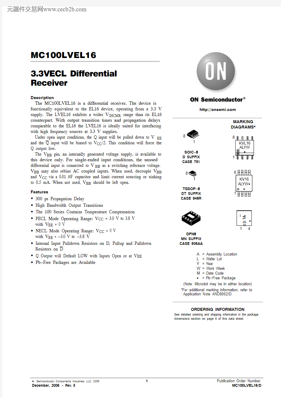
See detailed ordering and shipping information in the package dimensions section on page 6 of this data sheet.
ORDERING INFORMATION
https://www.doczj.com/doc/e66487702.html,
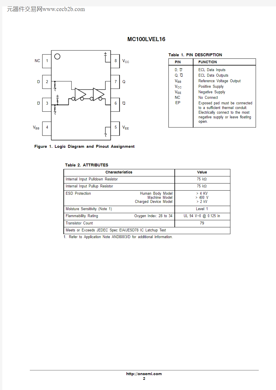
Figure 1. Logic Diagram and Pinout Assignment
Table 1. PIN DESCRIPTION
Q
V EE
V CC
D Q
D V BB
NC
Table 2. ATTRIBUTES
Characteristics
Value Internal Input Pulldown Resistor 75 k W Internal Input Pullup Resistor 75 k W ESD Protection
Human Body Model
Machine Model
Charged Device Model
> 4 KV > 400 V > 2 kV Moisture Sensitivity (Note 1)Level 1
Flammability Rating Oxygen Index: 28 to 34
UL 94 V ?0 @ 0.125 in
Transistor Count
79
Meets or Exceeds JEDEC Spec EIA/JESD78 IC Latchup Test 1.Refer to Application Note AND8003/D for additional information.
Table 3. MAXIMUM RATINGS
Symbol Parameter Condition 1Condition 2Rating Unit V CC PECL Mode Power Supply V EE = 0 V8 to 0V V EE NECL Mode Power Supply V CC = 0 V?8 to 0V
V I PECL Mode Input Voltage
NECL Mode Input Voltage V EE = 0 V
V CC = 0 V
V I V CC
V I V EE
6 to 0
?6 to 0
V
V
I out Output Current Continuous
Surge 50
100
mA
mA
I BB V BB Sink/Source± 0.5mA T A Operating Temperature Range?40 to +85°C T stg Storage Temperature Range?65 to +150°C
q JA Thermal Resistance (Junction?to?Ambient)0 LFPM
500 LFPM SO?8
SO?8
190
130
°C/W
°C/W
q JC Thermal Resistance (Junction?to?Case)Standard Board SO?841 to 44 ± 5%°C/W
q JA Thermal Resistance (Junction?to?Ambient)0 LFPM
500 LFPM TSSOP?8
TSSOP?8
185
140
°C/W
°C/W
q JC Thermal Resistance (Junction?to?Case)Standard Board TSSOP?841 to 44 ± 5%°C/W
q JA Thermal Resistance (Junction?to?Ambient)0 lfpm
500 lfpm DFN8
DFN8
129
84
°C/W
°C/W
T sol Wave Solder Pb
Pb?Free <2 to 3 sec @ 248°C
<2 to 3 sec @ 260°C
265
265
°C
Stresses exceeding Maximum Ratings may damage the device. Maximum Ratings are stress ratings only. Functional operation above the Recommended Operating Conditions is not implied. Extended exposure to stresses above the Recommended Operating Conditions may affect device reliability.
Table 4. LVPECL DC CHARACTERISTICS V CC= 3.3 V; V EE= 0.0 V (Note 2)
Symbol Characteristic
?40°C25°C85°C
Unit Min Typ Max Min Typ Max Min Typ Max
I EE Power Supply Current172317231824mA V OH Output HIGH Voltage (Note 3)221522952420227523452420227523452420mV V OL Output LOW Voltage (Note 3)147016051745149015951680149015951680mV V IH Input HIGH Voltage (Single?Ended)213524202135242021352420mV V IL Input LOW Voltage (Single?Ended)149018251490182514901825mV V BB Output Voltage Reference 1.92 2.04 1.92 2.04 1.92 2.04V V IHCMR Input HIGH Voltage Common Mode
Range (Differential) (Note 4)
Vpp < 500 mV
Vpp y 500 mV 1.2
1.5
2.9
2.9
1.1
1.4
2.9
2.9
1.1
1.4
2.9
2.9
V
V
I IH Input HIGH Current150150150m A
I IL Input LOW Current D
D
0.5
?600
0.5
?600
0.5
?600
m A
m A
NOTE:Device will meet the specifications after thermal equilibrium has been established when mounted in a test socket or printed circuit board with maintained transverse airflow greater than 500 lfpm. Electrical parameters are guaranteed only over the declared
operating temperature range. Functional operation of the device exceeding these conditions is not implied. Device specification limit values are applied individually under normal operating conditions and not valid simultaneously.
2.Input and output parameters vary 1:1 with V CC. V EE can vary ±0.3 V.
3.Outputs are terminated through a 50 W resistor to V CC? 2 V.
4.V IHCMR min varies 1:1 with V EE, max varies 1:1 with V CC. The V IHCMR range is referenced to the most positive side of the differential input signal.
Normal operation is obtained if the HIGH level falls within the specified range and the peak-to-peak voltage lies between V PP min and 1 V. Table 5. LVNECL DC CHARACTERISTICS V CC= 0.0 V; V EE= ?3.3 V (Note 5)
Symbol Characteristic
?40°C25°C85°C
Unit Min Typ Max Min Typ Max Min Typ Max
I EE Power Supply Current172317231824mA V OH Output HIGH Voltage (Note 6)?1085?1005?880?1025?955?880?1025?955?880mV V OL Output LOW Voltage (Note 6)?1830?1695?1555?1810?1705?1620?1810?1705?1620mV V IH Input HIGH Voltage (Single?Ended)?1165?880?1165?880?1165?880mV V IL Input LOW Voltage (Single?Ended)?1810?1475?1810?1475?1810?1475mV V BB Output Voltage Reference?1.38?1.26?1.38?1.26?1.38?1.26V V IHCMR Input HIGH Voltage Common Mode
Range (Differential) (Note 7)
Vpp < 500 mV
Vpp y 500 mV ?2.1
?1.8
?0.4
?0.4
?2.2
?1.9
?0.4
?0.4
?2.2
?1.9
?0.4
?0.4
V
V
I IH Input HIGH Current150150150m A
I IL Input LOW Current D
D
0.5
?600
0.5
?600
0.5
?600
m A
m A
NOTE:Device will meet the specifications after thermal equilibrium has been established when mounted in a test socket or printed circuit board with maintained transverse airflow greater than 500 lfpm. Electrical parameters are guaranteed only over the declared
operating temperature range. Functional operation of the device exceeding these conditions is not implied. Device specification limit values are applied individually under normal operating conditions and not valid simultaneously.
5.Input and output parameters vary 1:1 with V CC. V EE can vary ±0.3 V.
6.Outputs are terminated through a 50 W resistor to V CC? 2 V.
7.V IHCMR min varies 1:1 with V EE, max varies 1:1 with V CC. The V IHCMR range is referenced to the most positive side of the differential input signal.
Normal operation is obtained if the HIGH level falls within the specified range and the peak-to-peak voltage lies between V PP min and 1 V.
Table 6. AC CHARACTERISTICS V CC = 3.3 V; V EE = 0.0 V or V CC = 0.0 V; V EE = ?3.3 V (Note 8)
Symbol Characteristic
?40°C
25°C 85°C Unit Min
Typ Max
Min
Typ Max
Min
Typ Max
f max
Maximum Toggle Frequency 1.75 1.75 1.75GHz t PLH t PHL Propagation Delay to Output
Differential Single ?Ended
150100275275400450225175
300300375425240190
315315390440ps
t SKEW Duty Cycle Skew (Differential)(Note 9)530
520
520ps t JITTER Random Clock Jitter (RMS)0.7
0.7
0.7
ps V PP Input Swing (Note 10)150100015010001501000mV t r t f
Output Rise/Fall Times Q (20% ? 80%)
120
220
320
120
220
320
120
220
320ps
NOTE:Device will meet the specifications after thermal equilibrium has been established when mounted in a test socket or printed circuit
board with maintained transverse airflow greater than 500 lfpm. Electrical parameters are guaranteed only over the declared
operating temperature range. Functional operation of the device exceeding these conditions is not implied. Device specification limit values are applied individually under normal operating conditions and not valid simultaneously.
8.V EE can vary ±0.3 V.
9.Duty cycle skew is the difference between a t PLH and t PHL propagation delay through a device.
10.V PP(min) is minimum input swing for which AC parameters guaranteed. The device has a DC gain of ≈40.
Figure 2. Typical Termination for Output Driver and Device Evaluation (See Application Note AND8020/D ? Termination of ECL Logic Devices.)
V TT
V TT = V CC ? 2.0 V
ORDERING INFORMATION
Device Package Shipping?
MC100LVEL16D SO?898 Units / Rail
98 Units / Rail
MC100LVEL16DG SO?8
(Pb?Free)
MC100LVEL16DR2SO?82500 Tape & Reel
2500 Tape & Reel
MC100LVEL16DR2G SO?8
(Pb?Free)
MC100LVEL16DT TSSOP?8100 Units / Rail
100 Units / Rail
MC100LVEL16DTG TSSOP?8
(Pb?Free)
MC100LVEL16DTR2TSSOP?82500 Tape & Reel
2500 Tape & Reel
MC100LVEL16DTR2G TSSOP?8
(Pb?Free)
MC100LVEL16MNR4DFN81000 / Tape & Reel
1000 / Tape & Reel
MC100LVEL16MNR4G DFN8
(Pb?Free)
?For information on tape and reel specifications, including part orientation and tape sizes, please refer to our Tape and Reel Packaging Specifications Brochure, BRD8011/D.
Resource Reference of Application Notes
AN1405/D?ECL Clock Distribution Techniques
AN1406/D?Designing with PECL (ECL at +5.0 V)
AN1503/D?ECLinPS t I/O SPiCE Modeling Kit
AN1504/D?Metastability and the ECLinPS Family
AN1568/D?Interfacing Between LVDS and ECL
AN1672/D?The ECL Translator Guide
AND8001/D?Odd Number Counters Design
AND8002/D?Marking and Date Codes
AND8020/D?Termination of ECL Logic Devices
AND8066/D?Interfacing with ECLinPS
AND8090/D?AC Characteristics of ECL Devices
PACKAGE DIMENSIONS
SOIC?8 NB
CASE 751?07
ISSUE AH
NOTES:
1.DIMENSIONING AND TOLERANCING PER
ANSI Y14.5M, 1982.
2.CONTROLLING DIMENSION: MILLIMETER.
3.DIMENSION A AND B DO NOT INCLUDE
MOLD PROTRUSION.
4.MAXIMUM MOLD PROTRUSION 0.15 (0.006)
PER SIDE.
5.DIMENSION D DOES NOT INCLUDE DAMBAR
PROTRUSION. ALLOWABLE DAMBAR
PROTRUSION SHALL BE 0.127 (0.005) TOTAL
IN EXCESS OF THE D DIMENSION AT
MAXIMUM MATERIAL CONDITION.
6.751?01 THRU 751?06 ARE OBSOLETE. NEW
STANDARD IS 751?
07.
DIM
A
MIN MAX MIN MAX
INCHES
4.80
5.000.1890.197
MILLIMETERS
B 3.80 4.000.1500.157
C 1.35 1.750.0530.069
D0.330.510.0130.020
G 1.27 BSC0.050 BSC
H0.100.250.0040.010
J0.190.250.0070.010
K0.40 1.270.0160.050
M0 8 0 8
N0.250.500.0100.020
S 5.80 6.200.2280.244 Y
M
0.25 (0.010)Z S X S
____
ǒmm
inches
ǔ
SCALE 6:1
*For additional information on our Pb?Free strategy and soldering
details, please download the ON Semiconductor Soldering and
Mounting Techniques Reference Manual, SOLDERRM/D.
SOLDERING FOOTPRINT*
PACKAGE DIMENSIONS
DIM MIN MAX MIN MAX INCHES
MILLIMETERS A 2.90 3.100.1140.122B 2.90 3.100.1140.122C 0.80 1.100.0310.043D 0.050.150.0020.006F 0.400.700.0160.028G 0.65 BSC 0.026 BSC L 4.90 BSC 0.193 BSC M
0 6 0 6 __
__
K 0.250.400.0100.016TSSOP ?8DT SUFFIX
PLASTIC TSSOP PACKAGE
CASE 948R ?02
ISSUE A
NOTES:
1.DIMENSIONING AND TOLERANCING PER ANSI Y14.5M, 198
2.
2.CONTROLLING DIMENSION: MILLIMETER.
3.DIMENSION A DOES NOT INCLUDE MOLD FLASH.PROTRUSIONS OR GATE BURRS. MOLD FLASH OR GATE BURRS SHALL NOT EXCEED 0.15(0.006) PER SIDE.
4.DIMENSION B DOES NOT INCLUDE INTERLEAD FLASH OR PROTRUSION. INTERLEAD FLASH OR PROTRUSION SHALL NOT EXCEED 0.25 (0.010)PER SIDE.
5.TERMINAL NUMBERS ARE SHOWN FOR REFERENCE ONLY.
6.DIMENSION A AND B ARE TO BE DETERMINED AT DATUM PLANE ?W?.
PACKAGE DIMENSIONS
DFN8
CASE 506AA ?01
ISSUE D
BOTTOM VIEW
8 X
ON Semiconductor and are registered trademarks of Semiconductor Components Industries, LLC (SCILLC). SCILLC reserves the right to make changes without further notice to any products herein. SCILLC makes no warranty, representation or guarantee regarding the suitability of its products for any particular purpose, nor does SCILLC assume any liability arising out of the application or use of any product or circuit, and specifically disclaims any and all liability, including without limitation special, consequential or incidental damages.“Typical” parameters which may be provided in SCILLC data sheets and/or specifications can and do vary in different applications and actual performance may vary over time. All operating parameters, including “Typicals” must be validated for each customer application by customer’s technical experts. SCILLC does not convey any license under its patent rights nor the rights of others. SCILLC products are not designed, intended, or authorized for use as components in systems intended for surgical implant into the body, or other applications intended to support or sustain life, or for any other application in which the failure of the SCILLC product could create a situation where personal injury or death may occur. Should Buyer purchase or use SCILLC products for any such unintended or unauthorized application, Buyer shall indemnify and hold SCILLC and its officers, employees, subsidiaries, affiliates,and distributors harmless against all claims, costs, damages, and expenses, and reasonable attorney fees arising out of, directly or indirectly, any claim of personal injury or death associated with such unintended or unauthorized use, even if such claim alleges that SCILLC was negligent regarding the design or manufacture of the part. SCILLC is an Equal Opportunity/Affirmative Action Employer. This literature is subject to all applicable copyright laws and is not for resale in any manner.
PUBLICATION ORDERING INFORMATION
ECLinPS is a trademark of Semiconductor Components INdustries, LLC (SCILLC).