■RS-485 or RS-422 Quad Differential Line Receivers
■Operates from a single +3.3V supply ■Interoperable with +5.0V logic ■Tri-state Output Control
■-7V to +12V Common-Mode Input Voltage Range
■Common Driver Enable Control (SP3488)
■Independent Driver Enable Controls for each pair of Drivers (SP3489)■Compatibility with LTC488and SN75173 (SP3488)■Compatibility with LTC489and SN75175 (SP3489)
DESCRIPTION…
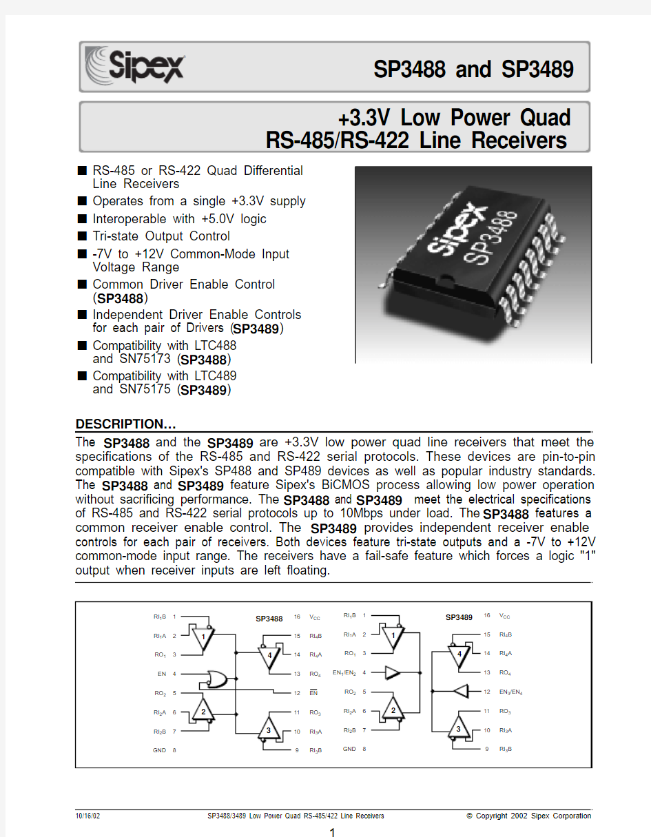
The SP3488 and the SP3489 are +3.3V low power quad line receivers that meet the specifications of the RS-485 and RS-422 serial protocols. These devices are pin-to-pin compatible with Sipex's SP488 and SP489 devices as well as popular industry standards.The SP3488 and SP3489 feature Sipex's BiCMOS process allowing low power operation without sacrificing performance. The SP3488 and SP3489 meet the electrical specifications of RS-485 and RS-422 serial protocols up to 10Mbps under load. The SP3488 features a common receiver enable control. The SP3489 provides independent receiver enable controls for each pair of receivers. Both devices feature tri-state outputs and a -7V to +12V common-mode input range. The receivers have a fail-safe feature which forces a logic "1"output when receiver inputs are left floating.
ABSOLUTE MAXIMUM RATINGS
These are stress ratings only and functional operation of the device at these or any other above those indicated in the operation sections of the specifications below is not implied. Exposure to absolute maximum rating conditions for extended periods of time may affect reliability.
V CC .........................................................................................+6.0V Input Voltages
Logic ......................................................................–0.3V to +6.0V Receiver ...............................................................................±14V Receiver Output Voltage..........................................–0.3V to +6.0V Input Currents
Logic ..................................................................................±25mA Storage Temperature............................................–65°C to +150°C Power Dissipation
Plastic DIP ........................................................................375mW (derate 7mW/°C above +70°C)
Small Outline ....................................................................375mW (derate 7mW/°C above +70°C)
Lead Temperature (soldering, 10 sec)...................................300°
C
SPECIFICATIONS
V = +3.3V ±5%; typicals at 25°C; T ≤ T ≤ T unless otherwise noted.
Figure 1. Timing Test Circuit Figure 2. Enable/Disable Timing Test Circuit
Pin 6 — RI 2A — Receiver 2 input A.Pin 7 — RI 2B — Receiver 2 input B.Pin 8 — GND — Digital Ground.Pin 9 — RI 3B — Receiver 3 input B.Pin 10 — RI 3A — Receiver 3 input A.Pin 11 — RO 3 — Receiver 3 Output — If Receiver 3 output is enabled, if RI 3A > RI 3B by 200mV, Receiver 3 output is high. If Receiver 3output is enabled, and if RI 3A < RI 3B by 200mV, Receiver 3 output is low.
Pin 12 — EN — Receiver Output Enable. Please refer to SP3488 Truth Table (1).
SP3488 PINOUT
Pin 1 — RI 1B — Receiver 1 input B.Pin 2 — RI 1A — Receiver 1 input A.
Pin 3 — RO 1 — Receiver 1 Output — If Re-ceiver 1 output is enabled, if RI 1A > RI 1B by 200mV, Receiver output is high. If Receiver 1output is enabled, and if RI 1A < RI 1B by 200mV,Receiver 1 output is low.
Pin 4 — EN — Receiver Output Enable. Please refer to SP3488 Truth Table (1).
Pin 5 — RO 2 — Receiver 2 Output — If Re-ceiver 2 output is enabled, if RI 2A > RI 2B by 200mV, Receiver 2 output is high. If Receiver 2output is enabled, and if RI 2A < RI 2B by 200mV, Receiver 2 output is low.
PINOUT
Pin 13 — RO 4 — Receiver 4 Output — If Receiver 4 output is enabled, if RI 4A > RI 4B by 200mV, Receiver 4 output is high. If Receiver 4output is enabled, and if RI 4A < RI 4B by 200mV, Receiver 4 output is low.Pin 14 — RI 4A — Receiver 4 input A.Pin 15 — RI 4B — Receiver 4 input B.Pin 16 — V CC — Positive Supply +3.00V < V CC < +3.60V
SP3489 PINOUT
Pin 1 — RI 1B — Receiver 1 input B.Pin 2 — RI 1A — Receiver 1 input A.Pin 3 — RO 1 — Receiver 1 Output — If Receiver 1 output is enabled, if RI 1A > RI 1B by 200mV, Receiver output is high. If Receiver 1output is enabled, and if RI 1A < RI 1B by 200mV,Receiver 1 output is low.
Pin 4 — EN1/EN2 — Receiver 1 and 2 Output Enable. Please refer to SP3489 Truth Table (2).Pin 5 — RO 2 — Receiver 2 Output — If Receiver 2 output is enabled, if RI 2A > RI 2B by 200mV, Receiver 2 output is high. If Receiver 2output is enabled, and if RI 2A < RI 2B by 200mV, Receiver 2 output is low.Pin 6 — RI 2A — Receiver 2 input A.Pin 7 — RI 2B — Receiver 2 input B.Pin 8 — GND — Digital Ground.
DIFFERENTIAL
ENABLES OUTPUT A – B EN EN RO
V ID ≥ 0.2V H X H X L H –0.2V < V ID < +0.2V
H X X X L X V ID ≤ 0.2V
H X L X L L X
L
H
Hi–Z
Table 1. SP3488 Truth Table Pin 9 — RI 3B — Receiver 3 input B.Pin 10 — RI 3A — Receiver 3 input A.Pin 11 — RO 3 — Receiver 3 Output — If Receiver 3 output is enabled, if RI 3A > RI 3B by 200mV, Receiver 3 output is high. If Receiver 3output is enabled, and if RI 3A < RI 3B by 200mV, Receiver 3 output is low.
Pin 12 — EN3/EN4 — Receiver 3 and 4 Output Enable. Please refer to SP3489 Truth Table (2).Pin 13 — RO 4 — Receiver 4 Output — If Receiver 4 output is enabled, if RI 4A > RI 4B by 200mV, Receiver 4 output is high. If Receiver 4output is enabled, and if RI 4A < RI 4B by 200mV, Receiver 4 output is low.Pin 14 — RI 4A — Receiver 4 input A.Pin 15 — RI 4B — Receiver 4 input B.Pin 16 — V CC — Positive Supply +3.00V < V CC < +3.60V
Table 2. SP3489 Truth Table
DIFFERENTIAL
ENABLES
OUTPUT A – B EN 1/EN 2 or EN 3/EN 4
RO
V ID ≥ 0.2V H H –0.2V < V ID < +0.2V
H X V ID ≤ 0.2V
H L X
L
Hi–Z
FEATURES...
The SP3488 and the SP3489 are +3.3V low power quad line receivers that meet the specifications of the RS-485 and RS-422 serial protocols. These devices are pin-to-pin compatible with Sipex's SP488 and SP489devices as well as popular industry standards.The SP3488 and SP3489 devices feature Sipex's BiCMOS process allowing low power operation without sacrificing performance.The RS-485 standard is ideal for multi-drop applications or for long distance interfaces.RS-485 allows up to 32 drivers and 32 receivers to be connected to a data bus, making it an ideal choice for multi-drop applications. Since the
cabling can be as long as 4,000 feet, RS-485 transceivers are equipped with a wide (-7V to +12V) common mode range to accomodate ground potential differences. Because the RS-485 protocol is a differential interface, data is virtually immune to noise in the transmission line.
Receiver...
The SP3488and the SP3489receivers have differential inputs with an input sensitivity as low as +100mV. Input impedance of the receivers is typically 15K? (12K? minimum).
A wide common mode range of -7V to +12V allows for large ground potential differences between systems.The SP3488 features active HIGH and active LOW common receiver enable controls. Refer to SP3488 Truth Table in Table 1. The SP3489 provides independent, active high receiver enable controls for each pair of receivers. Refer to SP3489 Truth Table in Table 2. Both devices feature tri-state outputs and a -7V to +12V common-mode input range permitting a +7V ground difference between devices on the communication bus. The SP3488and the SP3489 are equipped with a fail-safe feature which forces a logic HIGH at the receiver output when the input is left floating. The SP3488 and SP3489 receivers meet the electrical specifications of RS-485 and RS-422 serial protocol data rates up to 10Mbps under load.
AC PARAMETERS
V = +3.3V±5%; typicals at 25°C; T = 25°C unless otherwise noted.
Figure 3. Receiver Propagation Delays
Figure 4. Receiver Enable/Disable Timing
ORDERING INFORMATION
Quad RS485 Receivers:
Model....................................Enable/Disable...........................................................Temperature Range................................................Package https://www.doczj.com/doc/ed5598026.html,mon; active Low and Active High......................0°C to +70°C...........................................16–pin Plastic DIP https://www.doczj.com/doc/ed5598026.html,mon; active Low and Active High......................0°C to +70°C....................................................16–pin SOIC https://www.doczj.com/doc/ed5598026.html,mon; active Low and Active High......................–40°C to +85°C.......................................16–pin Plastic DIP https://www.doczj.com/doc/ed5598026.html,mon; active Low and Active High......................–40°C to +85°C................................................16–pin SOIC
SP3489CP...........................One per driver pair; active High.................................0°C to +70°C...........................................16–pin Plastic DIP SP3489CT............................One per driver pair; active High.................................0°C to +70°C....................................................16–pin SOIC SP3489EP............................One per driver pair; active High.................................–40°C to +85°C.......................................16–pin Plastic DIP SP3489ET............................One per driver pair; active High.................................–40°C to +85°C................................................16–pin SOIC
Please consult the factory for pricing and availability on a Tape-On-Reel option.
Corporation
SIGNAL PROCESSING EXCELLENCE
Sipex Corporation
Headquarters and
Sales Office
233 South Hillview Drive
Milpitas, CA 95035
TEL: (408) 934-7500
FAX: (408) 935-7600
Sales Office
22 Linnell Circle
Billerica, MA 01821
TEL: (978) 667-8700
FAX: (978) 670-9001
e-mail: sales@https://www.doczj.com/doc/ed5598026.html,
Sipex Corporation reserves the right to make changes to any products described herein. Sipex does not assume any liability arising out of the application or use of any product or circuit described hereing; neither does it convey any license under its patent rights nor the rights of others.