https://www.doczj.com/doc/e43220537.html,
FEATURES APPLICATIONS
DESCRIPTION
V
CANH
CANL
RXD
TXD
STB
SPLIT
SN65HVD1040
SLLS631B–MARCH2007–REVISED APRIL2007 LOW-POWER CAN TRANSCEIVER WITH BUS WAKE-UP
?Battery Operated Applications
?Improved Drop-in Replacement for the
TJA1040?Hand-Held Diagnostics
?Medical Scanning and Imaging
?±12kV ESD Protection
?HVAC
?Low-Current Standby Mode with Bus
?Security Systems
Wake-up:5μA Typical
?Telecom Base Station Status and Control ?Bus-Fault Protection of–27V to40V
?SAE J1939Standard Data Bus Interface ?Rugged Split-Pin Bus Stability
?NMEA2000Standard Data Bus Interface ?Dominant Time-Out Function
?ISO11783Standard Data Bus Interface ?Power-Up/Down Glitch-Free Bus Inputs and
?Industrial Automation
Outputs
–DeviceNet?Data Buses –High Input Impedance with Low V CC
–Monotonic Outputs During Power Cycling
?DeviceNet Vendor ID#806
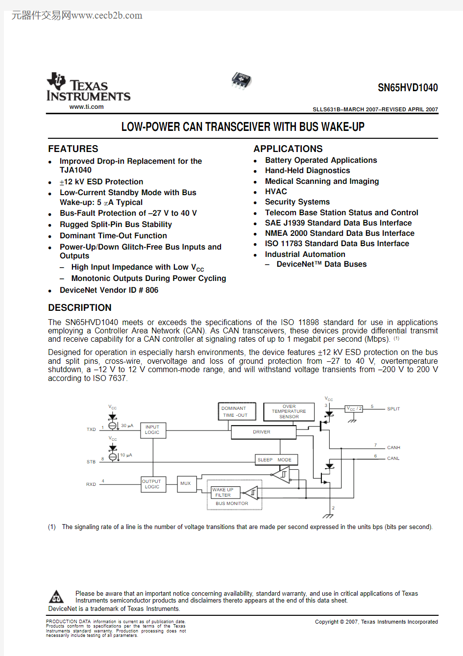
The SN65HVD1040meets or exceeds the specifications of the ISO11898standard for use in applications employing a Controller Area Network(CAN).As CAN transceivers,these devices provide differential transmit and receive capability for a CAN controller at signaling rates of up to1megabit per second(Mbps).(1) Designed for operation in especially harsh environments,the device features±12kV ESD protection on the bus and split pins,cross-wire,overvoltage and loss of ground protection from–27to40V,overtemperature shutdown,a–12V to12V common-mode range,and will withstand voltage transients from–200V to200V according to ISO7637.
(1)The signaling rate of a line is the number of voltage transitions that are made per second expressed in the units bps(bits per second).
Please be aware that an important notice concerning availability,standard warranty,and use in critical applications of Texas
Instruments semiconductor products and disclaimers thereto appears at the end of this data sheet.
https://www.doczj.com/doc/e43220537.html,
V SN65HVD1040
SN65HVD1040
SLLS631B–MARCH 2007–REVISED APRIL 2007
These devices have limited built-in ESD protection.The leads should be shorted together or the device placed in conductive foam during storage or handling to prevent electrostatic damage to the MOS gates.
The STB input (pin 8)selects between two different modes of operation;high-speed or low-power mode.The high-speed mode of operation is selected by connecting STB to ground.
If a high logic level is applied to the STB pin of the SN65HVD1040,the device enters a low-power bus-monitor standby mode.While the SN65HVD1040is in the low-power bus-monitor standby mode,a dominant bit greater than 5μs on the bus is passed by the bus-monitor circuit to the receiver output.The local protocol controller may then reactivate the device when it needs to transmit to the bus.
A dominant-time-out circuit in the SN65HVD1040prevents the driver from blocking network communication during a hardware or software failure.The time-out circuit is triggered by a falling edge on TXD (pin 1).If no rising edge is seen before the time-out constant of the circuit expires,the driver is disabled.The circuit is then reset by the next rising edge on TXD.
The SPLIT output (pin 5)is available on the SN65HVD1040as a V CC /2common-mode bus voltage bias for a split-termination network.
The SN65HVD1040is characterized for operation from –40°C to 125°C.
ORDERING INFORMATION
DOMINANT LOW-POWER MARKED PART NUMBER PACKAGE (1)
ORDERING NUMBER TIME-OUT
BUS MONITOR
AS SN65HVD1040D (rail)SN65HVD1040YES
YES
SOIC-8
VP1040
SN65HVD1040DR (reel)
(1)
For the most current package and ordering information,see the Package Option Addendum at the end of this document,or see the TI website at https://www.doczj.com/doc/e43220537.html, .
https://www.doczj.com/doc/e43220537.html,
ABSOLUTE MAXIMUM RATINGS(1) RECOMMENDED OPERATING CONDITIONS
SUPPLY CURRRENT
DEVICE SWITCHING CHARACTERISTICS
SN65HVD1040 SLLS631B–MARCH2007–REVISED APRIL2007
VALUE
V CC Supply voltage(2)–0.3V to7V
V I(bus)Voltage range at any bus terminal(CANH,CANL,SPLIT)–27V to40V
I O(OUT)Receiver output current-20mA to20mA
Voltage input,transient pulse(3),(CANH,CANL,SPLIT)–200V to200V
Human Body Model Bus terminals and GND±12kV
Human body model(4)All pins±4kV
ESD
Charged-device-model(5)All pins±1kV
Machine model±200V
V I Voltage input range(TXD,STB)–0.5V to6V
T J Junction temperature–55°C to170°C
(1)Stresses beyond those listed under"absolute maximum ratings"may cause permanent damage to the device.These are stress ratings
only and functional operation of the device at these or any other conditions beyond those indicated under"recommended operating conditions"is not implied.Exposure to absolute-maximum-rated conditions for extended periods may affect device reliability.
(2)All voltage values,except differential I/O bus voltages,are with respect to network ground terminal.
(3)Tested in accordance with ISO7637,test pulses1,2,3a,3b,5,6&7.
(4)Tested in accordance JEDEC Standard22,Test Method A114-A.
(5)Tested in accordance JEDEC Standard22,Test Method C101.
MIN NOM MAX UNIT V CC Supply voltage 4.75 5.25V
V I or V IC Voltage at any bus terminal(separately or common mode)–12(1)12V
V IH High-level input voltage2 5.25V
TXD,STB
V IL Low-level input voltage00.8V
V ID Differential input voltage–66V
Driver–70
I OH High-level output current mA
Receiver–2
Driver70
I OL Low-level output current mA
Receiver2
t SS Maximum pulse width to remain in standby0.7μs
T J Junction temperature–40150 C (1)The algebraic convention,in which the least positive(most negative)limit is designated as minimum is used in this data sheet.
over operating free-air temperature range(unless otherwise noted)
PARAMETER TEST CONDITIONS MIN TYP MAX UNIT
Dominant V I=0V,60?Load,STB at0V5070
mA
I CC Supply current,V CC Recessive V I=V CC,STB at0V610
Standby STB at VCC,VI=VCC512μA
over recommended operating conditiions(unless otherwise noted)
TEST MIN TYP MAX UNIT
PARAMETER
CONDITIONS
t loop1Total loop delay,driver input to receiver output,Recessive to Dominant90230
STB at0V,
ns
See Figure9
t loop2Total loop delay,driver input to receiver output,Dominant to Recessive90230
https://www.doczj.com/doc/e43220537.html,
DRIVER ELECTRICAL CHARACTERISTICS
DRIVER SWITCHING CHARACTERISTICS
SN65HVD1040
SLLS631B–MARCH 2007–REVISED APRIL 2007
over recommended operating conditiions (unless otherwise noted)
PARAMETER
TEST CONDITIONS
MIN TYP (1)MAX UNIT CANH 2.9 3.4
4.5Bus output voltage V I =0V,STB at 0V,R L =60?,See Figure 1and V O(D)V (Dominant)
Figure 2
CANL
0.8 1.75V O(R)Bus output voltage (Recessive)V I =3V,STB at 0V,See Figure 1and Figure 22 2.53V V O Bus output voltage (Standby)
R L =60?,STB at V CC ,See Figure 1and Figure 2–0.10.1V
V I =0V,R L =60?,STB at 0V,See Figure 1and 1.53
Figure 2,and Figure 3
V OD(D)
Differential output voltage (Dominant)
V V I =0V,R L =45?,STB at 0V,See Figure 1and 1.43
Figure 2
Output symmetry (Dominant or V SYM STB at 0V,See Figure 2and Figure 13
0.9×V CC V CC 1.1×V CC
V Recessive)[V O(CANH)+V O(CANL))
V I =3V,R L =60?,STB at 0V,See Figure 1and
–0.0120.012Figure 2
V OD(R)Differential output voltage (Recessive)V
V I =3V,STB at 0V,No Load –0.50.05Common-mode output voltage V OC(D)2
2.33
(Dominant)
STB at 0V,See Figure 8
V Peak-to-peak common-mode output V OC(pp)0.3
voltage
I IH High-level input current,TXD input V I at V CC –22μA I IL Low-level input current,TXD input V I at 0V
–50
–10μA I O(off)
Power-off TXD Leakage current
V CC at 0V,TXD at 5V
1
μA
V CANH =–12V,CANL Open,See Figure 12
–120
–72V CANH =12V,CANL Open,See Figure 120.361
Short-circuit steady-state output I OS(ss)
mA
current
V CANL =–12V,CANH Open,See Figure 12–1–0.5V CANL =12V,CANH Open,See Figure 12
71
120See Input capacitance to ground in RECEIVER C O Output capacitance
ELECTRICAL CHARACTERISTICS .
(1)
All typical values are at 25 C with a 5-V supply.
over recommended operating conditions (unless otherwise noted)
PARAMETER
TEST CONDITIONS
MIN TYP MAX UNIT
t PLH Propagation delay time,low-to-high-level output 2565120t PHL Propagation delay time,high-to-low-level output 25
45
120t sk(p)Pulse skew (|t PHL –t PLH |)STB at 0V,See Figure 4
25
ns t r Differential output signal rise time 25t f Differential output signal fall time
50
t en Enable time from silent mode to dominant See Figure 710μs t dom
Dominant time-out
See Figure 10
300
450
700
μs
https://www.doczj.com/doc/e43220537.html,
RECEIVER ELECTRICAL CHARACTERISTICS RECEIVER SWITCHING CHARACTERISTICS
SPLIT-PIN CHARACTERISTICS
STB-PIN CHARACTERISTICS
SN65HVD1040 SLLS631B–MARCH2007–REVISED APRIL2007
over recommended operating conditions(unless otherwise noted)
PARAMETER TEST CONDITIONS MIN TYP(1)MAX UNIT
Positive-going input threshold
V IT+800900 voltage
STB at0V,See Table1
High-speed
Negative-going input threshold
V IT–mode500650mV voltage
V hys Hysteresis voltage(V IT+–V IT–)STB at V CC100125
V IT Input threshold voltage Standby mode STB at V CC5001150
V OH High-level output voltage I O=–2mA,See Figure64 4.6V
V OL Low-level output voltage I O=2mA,See Figure60.20.4V
CANH or CANL=5V,V CC at0V,
I I(off)Power-off bus input current5μA
TXD at0V
I O(off)Power-off RXD leakage current V CC at0V,RXD at5V20μA
C I Input capacitance to ground,(CANH or CANL)TX
D at3V,V I=0.4sin(4E6πt)+2.5V20pF
C I
D Differential input capacitance TXD at3V,V I=0.4sin(4E6πt)10pF
R ID Differential input resistance TXD at3V,STD at0V3080
k?R IN Input resistance,(CANH or CANL)TXD at3V,STD at0V153040
Input resistance matching
R I(m)V CANH=V CANL–3%0%3% [1–(R IN(CANH)/R IN(CANL))]x100%
(1)All typical values are at25 C with a5-V supply.
over recommended operating conditiions(unless otherwise noted)
PARAMETER TEST CONDITIONS MIN TYP MAX UNIT
t pLH Propagation delay time,low-to-high-level output60100130
t pHL Propagation delay time,high-to-low-level output4570130
STB at0V,TXD at3V,See
ns
Figure6
t r Output signal rise time8
t f Output signal fall time8
t BUS Dominant time required on bus for wake-up from
STB at V CC Figure110.75μs standby(1)
(1)The device under test shall not signal a wake-up condition with dominant pulses shorter than t BUS(min)and shall signal a wake-up
condition with dominant pulses longer than t BUS(max).Dominant pulses with a length between t BUS(min)and t BUS(max)may lead to a wake-up.
over recommended operating conditiions(unless otherwise noted)
PARAMETER TEST CONDITIONS MIN TYP MAX UNIT V O Output voltage–500μA
I O(stb)Standby mode leakage current STB at2V,–12V≤V O≤12V–55μA
over recommended operating conditiions(unless otherwise noted)
PARAMETER TEST CONDITIONS MIN TYP MAX UNIT I IH High level input current STB at2V–100μA
I IL Low level input current STB at0V–100μA
https://www.doczj.com/doc/e43220537.html,
PARAMETER MEASUREMENT INFORMATION
2.5 V
3.5 V 1.5 V
Recessive
Dominant
O (CANH)
V O (CANL)
V
I
?2 V 3 V TEST 3 7 V
V O(D)
O(R)
+20%
V CC V I V I I O
V I(CANH) + V I(CANL)
2
V IC =
SN65HVD1040
SLLS631B–MARCH 2007–REVISED APRIL 2007
Figure 1.Driver Voltage,Current,and Test Definition
Figure 2.Bus Logic State Voltage Definitions
Figure 3.Driver V OD Test Circuit
Figure 4.Driver Test Circuit and Voltage Waveforms
Figure 5.Receiver Voltage and Current Definitions
https://www.doczj.com/doc/e43220537.html,
O
OH
V
OL
C L= 15 pF20%
(see Note B)
CC
60 W+1%
V CC
0 V
V OH
V OL
V I
SN65HVD1040
SLLS631B–MARCH2007–REVISED APRIL2007 PARAMETER MEASUREMENT INFORMATION(continued)
A.The input pulse is supplied by a generator having the following characteristics:PRR≤125kHz,50%duty cycle,t r≤
6ns,t f≤6ns,Z O=50?.
B.C L includes instrumentation and fixture capacitance within 20%.
Figure6.Receiver Test Circuit and Voltage Waveforms
Table1.Differential Input Voltage Threshold Test
INPUT OUTPUT
V CANH V CANL|V ID|R
–11.1V–12V900mV L V OL
12V11.1V900mV L
–6V–12V6V L
12V6V6V L
–11.5V–12V500mV H V OH
12V11.5V500mV H
–12V–6V6V H
6V12V6V H
Open Open X H
Figure7.t en Test Circuit and Voltage Waveforms
A.All V I input pulses are from0V to V CC and supplied by a generator having the following characteristics:t r or t f≤6ns.
Pulse Repetition Rate(PRR)=125kHz,50%duty cycle.
Figure8.Peak-to-Peak Common Mode Output Voltage Test and Waveform
https://www.doczj.com/doc/e43220537.html,
60 W +1%
V CC
0 V
V OH
V
OL V I
V O
V CC
0 V OD(D)
O
V V OH
OL
0.7m SN65HVD1040
SLLS631B–MARCH 2007–REVISED APRIL 2007
A.
All V I input pulses are from 0V to V CC and supplied by a generator with the following characteristics:t r or t f ≤6ns.Pulse Repetition Rate (PRR)=125kHz,50%duty cycle.
Figure 9.t loop Test Circuit and Voltage Waveforms
A.All V I input pulses are from 0V to V CC and supplied by a generator with the following characteristics:t r or t f ≤6ns.Pulse Repetition Rate (PRR)=500Hz,50%duty cycle.
B.
C L =100pF includes instrumentation and fixture capacitance within 20%.
Figure 10.Dominant Time-Out Test Circuit and Waveform
A.For V I bit width ≤0.7μs,V O =V OH .For V I I bit width ≥5μs,V O =V OL .V I input pulses are supplied from a generator with the following characteristics;t r or t f ≤6ns.Pulse Repetition Rate (PRR)=50Hz,30%duty cycle.
B.
C L =15pF includes instrumentation and fixture capacitance within 20%.
Figure 11.t BUS Test Circuit and Waveform
https://www.doczj.com/doc/e43220537.html,
0 V or V V I
SYM =
+O
(CANL)
V O (CANH)
V SN65HVD1040
SLLS631B–MARCH 2007–REVISED APRIL 2007
Figure 12.Driver Short-Circuit Current Test and Waveform
Figure 13.Driver Output Symmetry Test Circuit
https://www.doczj.com/doc/e43220537.html,
DEVICE INFORMATION
THERMAL CHARACTERISTICS
SN65HVD1040
SLLS631B–MARCH 2007–REVISED APRIL 2007
Table 2.DRIVER FUNCTION TABLE (1)
INPUTS OUTPUTS BUS STATE
TXD STB CANH
CANL L L H L DOMINANT H L Z Z RECESSIVE Open X Z Z RECESSIVE X H or Open
Z
Z
RECESSIVE (1)
H =high level;L =low level;X =irrelevant;Z =high impedance
Table 3.RECEIVER FUNCTION TABLE (1)
DIFFERENTIAL INPUTS STB OUTPUT BUS STATE V ID =CANH -CANL
RXD
V ID ≥0.9V L L DOMINANT V ID ≥ 1.15V H or Open
L DOMINANT
0.5V X ??V ID ≤0.5V X H RECESSIVE Open X H RECESSIVE (1) H =high level;L =low level;X =irrelevant;?=indeterminate;Z =high impedance over operating free-air temperature range (unless otherwise noted) PARAMETER TEST CONDITIONS MIN TYP MAX UNIT Low-K Thermal Resistance (1)211°C/W θJA Thermal Resistance,Junction-to-Air High-K Thermal Resistance 131°C/W θJB Thermal Resistance,53Junction-to-Board °C/W θJC Thermal Resistance,79Junction-to-Case R L =60?,S at 0V, P D Device Power Dissipation 112170mW Input to TXD a 500kHz 50%duty-cycle square wave T JS Junction Temperature,Thermal Shutdown (2) 190 °C (1)Tested in accordance with the Low-K or High-K thermal metric definitions of EIA/JESD51-3for leaded surface mount packages.(2) Extended operation in thermal shutdown may affect device reliability,see the Application Information section. https://www.doczj.com/doc/e43220537.html, DEVICE INFORMATION SN65HVD1040 SLLS631B–MARCH2007–REVISED APRIL2007 Table4.Parametric Cross Reference With the TJA1040 TJA1040(1)PARAMETER HVD10xx TJA1040DRIVER SECTION V IH High-level input voltage Recommended V IH V IL Low-level input voltage Recommended V IL I IH High-level input current Driver I IH I IL Low-level input current Driver I IL TJA1040BUS SECTION V th(dif)Differential input voltage Receiver V IT and recommended V ID V hys(dif)Differential input hysteresis Receiver V hys V O(dom)Dominant output voltage Driver V O(D) V O(reces)Recessive output voltage Driver V O(R) V i(dif)(th)Differential input voltage Receiver V IT and recommended V ID V O(dif0(bus)Differential bus voltage Driver V OD(D)and V OD(R) I LI Power-off bus input current Receiver I I(off) I O(SC)Short-circuit output current Driver I OS(SS) R i(cm)CANH,CANL input resistance Receiver R IN R i(def)Differential input resistance Receiver R ID R i(cm)(m)Input resistance matching Receiver R I(m) C i(cm)Input capacitance to ground Receiver C I C i(dif)Differential input capacitance Receiver C ID TJA1040RECEIVER SECTION I OH High-level output current Recommended I OH I OL Low-level output current Recommended I OL TJA1040SPLIT PIN SECTION V O Reference output voltage V O TJA1040TIMING SECTION t d(TXD-BUSon)Delay TXD to bus active Driver t PLH t d(TXD-BUSoff)Delay TXD to bus inactive Driver t PHL t d(BUSon-RXD)Delay bus active to RXD Receiver t PHL t d(BUSoff-RXD)Delay bus inactive to RXD Receiver t PLH t PD(TXD–RXD)Prop delay TXD to RXD Device t LOOP1and t LOOP2 t d(stb-norm)Enable time from standby to dominant Driver t en TJA1040STB PIN SECTION V IH High-level input voltage Recommended V IH V IL Low-level input voltage Recommended V IL I IH High-level input current I IH I IL Low-level input current I IL (1)From TJA1040Product Specification,Philips Semiconductors,2003February19. https://www.doczj.com/doc/e43220537.html, Equivalent Input and Output Schematic Diagrams SN65HVD1040 SLLS631B–MARCH 2007–REVISED APRIL 2007 https://www.doczj.com/doc/e43220537.html, TYPICAL CHARACTERISTICS ?40 02570125 ?R e c e s s i v e -t o -D o m i n a n t L o o p T i m e ?n s t L O O P 1T A ?Free-Air T emperature ?°C ?4002570125 ?D o m i n a n t -t o -R e c e s s i v e L o o p T i m e ?n s t L O O P 2T A ?Free-Air T emperature ?°C ?10 01020304050607080900 12345 I O L ? L o w -L e v e l O u t p u t C u r r e n t ? m A V O CANL ? Low-Level Output Voltage ? V 5101520253035404550Signaling Rate ? kbps I C C ? R M S S u p p l y C u r r e n t ? m A SN65HVD1040 SLLS631B–MARCH 2007–REVISED APRIL 2007 RECESSIVE-TO-DOMINANT LOOP TIME DOMINANT-TO-RECESSIVE LOOP TIME vs vs FREE-AIR TEMPERATURE (across V CC ) FREE-AIR TEMPERATURE (across V CC ) Figure 14. Figure 15. SUPPLY CURRENT (RMS) DRIVER LOW-LEVEL OUTPUT VOLTAGE vs vs SIGNALING RATE LOW-LEVEL OUTPUT CURRENT Figure 16.Figure 17. https://www.doczj.com/doc/e43220537.html, -0 -10-20-30-40-50-60-70-80 01234 5I O H ?H i g h -L e v e l O u t p u t C u r r e n t ?m A V O CANH ?High-Level Output V oltage ?V 0.5 1 1.5 2 2.5 3?40 02570125 T A ? Free-Air Temperature ? °C D o m i n a n t D r i v e r D i f f e r e n t i a l O u t p u t V o l t a g e ? V I O ? D i f f e r e n t i a l D r i v e r O u t p u t C u r r e n t ? m A V CC ? Supply Voltage ? V 0.60.60.70.70.80.80.80.80.70.70.60.6? R e c e i v e r O u t p u t V o l t a g e ? V V O V ID ? Differential Input Voltage ? V SN65HVD1040 SLLS631B–MARCH 2007–REVISED APRIL 2007 TYPICAL CHARACTERISTICS (continued) DRIVER HIGH-LEVEL OUTPUT VOLTAGE DRIVER DIFFERENTIAL OUTPUT VOLTAGE vs vs HIGH-LEVEL OUTPUT CURRENT FREE-AIR TEMPERATURE (across V CC ) Figure 18. Figure 19. DRIVER OUTPUT CURRENT RECEIVER OUTPUT VOLTAGE vs vs SUPPLY VOLTAGE DIFFERENTIAL INPUT VOLTAGE Figure 20.Figure 21. https://www.doczj.com/doc/e43220537.html, D B V m 020 40 60 80 0.1 1 10 1001000 f ? Frequency ? MHz d B m SN65HVD1040 SLLS631B–MARCH 2007–REVISED APRIL 2007 TYPICAL CHARACTERISTICS (continued) TYPICAL ELECTROMAGNETIC EMISSIONS TYPICAL ELECTROMAGNETIC UP TO 50MHZ (Peak Amplitude) IMMUNITY PERFORMANCE Figure 22.Frequency Spectrum of Common-Mode Figure 23.Direct Power Injection (DPI)Response vs Emissions Frequency https://www.doczj.com/doc/e43220537.html, APPLICATION INFORMATION CAN Basics SN65HVD1040 SLLS631B–MARCH 2007–REVISED APRIL 2007 The basics of arbitration require that the receiver at the sending node designate the first bit as dominant or recessive after the initial wave of the first bit of a message travels to the most remote node on a network and back again.Typically,this “sample”is made at 75%of the bit width,and within this limitation,the maximum allowable signal distortion in a CAN network is determined by network electrical parameters. Factors to be considered in network design include the approximately 5ns/m propagation delay of typical twisted-pair bus cable;signal amplitude loss due to the loss mechanisms of the cable;and the number,length,and spacing of drop-lines (stubs)on a network.Under strict analysis,variations among the different oscillators in a system also need to be accounted for with adjustments in signaling rate and stub and bus length.Table 5lists the maximum signaling rates achieved with the SN65HVD1040with several bus lengths of category 5,shielded twisted pair (CAT 5STP)cable. Table 5.Maximum Signaling Rates for Various Cable Lengths Bus Length (m) Signaling Rate (kbps) 3010001005002502505001251000 62.5 The ISO 11898Standard specifies a maximum bus length of 40m and maximum stub length of 0.3m with a maximum of 30nodes.However,with careful design,users can have longer cables,longer stub lengths,and many more nodes to a bus.(Note:Non-standard application may come with a trade-off in signaling rate.)A large number of nodes requires a transceiver with high input impedance such as the HVD1040. The Standard specifies the interconnect to be a single twisted-pair cable (shielded or unshielded)with 120?characteristic impedance (Z O ).Resistors equal to the characteristic impedance of the line terminate both ends of the cable to prevent signal reflections.Unterminated drop-lines connect nodes to the bus and should be kept as short as possible to minimize signal reflections. Connectors,while not specified by the standard should have as little effect as possible on standard operating parameters such as capacitive loading.Although unshielded cable is used in many applications,data transmission circuits employing CAN transceivers are usually used in applications requiring a rugged interconnection with a wide common-mode voltage range.Therefore,shielded cable is recommended in these electronically harsh environments,and when coupled with the Standard’s –2-V to 7-V common-mode range of tolerable ground noise,helps to ensure data integrity.The HVD1040enhances the Standard’s insurance of data integrity with an extended –12V to 12V range of common-mode operation. https://www.doczj.com/doc/e43220537.html, 500mV Threshold mV Threshold ALLOWABLE JITTER NOISE MARGIN W 120W m F SN65HVD1040 SLLS631B–MARCH 2007–REVISED APRIL 2007 Figure 24.Typical CAN Differential Signal Eye-Pattern An eye pattern is a useful tool for measuring overall signal quality.As displayed in Figure 25,the differential signal changes logic states in two places on the display,producing an “eye.”Instead of viewing only one logic crossing on the scope,an entire “bit”of data is brought into view.The resulting eye pattern includes all of the effects of systemic and random distortion,and displays the time during which a signal may be considered valid.The height of the eye above or below the receiver threshold voltage level at the sampling point is the noise margin of the system.Jitter is typically measured at the differential voltage zero-crossing during the logic state transition of a signal.Note that jitter present at the receiver threshold voltage level is considered by some to be a more effective representation of the jitter at the input of a receiver. As the sum of skew and noise increases,the eye closes and data is corrupted.Closing the width decreases the time available for accurate sampling,and lowering the height enters the 900mV or 500mV threshold of a receiver. Different sources induce noise onto a signal.The more obvious noise sources are the components of a transmission circuit themselves;the signal transmitter,traces and cables,connectors,and the receiver.Beyond that,there is a termination dependency,cross-talk from clock traces and other proximity effects,V CC and ground bounce,and electromagnetic interference from near-by electrical equipment. The balanced receiver inputs of the HVD1040mitigate most all sources of signal corruption,and when used with a quality shielded twisted-pair cable,help insure data integrity. Figure 25.Typical HVD1040Application https://www.doczj.com/doc/e43220537.html, Thermal Shutdown SN65HVD1040 SLLS631B–MARCH 2007–REVISED APRIL 2007 The SN65HVD1040has a thermal shutdown that turns off the driver outputs when the junction temperature nears 190°C.This shutdown prevents catastrophic failure from bus shorts,but does not protect the circuit from possible damage.The user should strive to maintain recommended operating conditions,and not exceed absolute maximum ratings at all times.If the SN65HVD1040is subjected to many or long durations faults that can put the device into thermal shutdown,it should be replaced. PACKAGING INFORMATION Orderable Device Status (1)Package Type Package Drawing Pins Package Qty Eco Plan (2) Lead/Ball Finish MSL Peak Temp (3)SN65HVD1040D ACTIVE SOIC D 875Green (RoHS &no Sb/Br)CU NIPDAU Level-1-260C-UNLIM SN65HVD1040DG4ACTIVE SOIC D 875 Green (RoHS &no Sb/Br) CU NIPDAU Level-1-260C-UNLIM SN65HVD1040DR ACTIVE SOIC D 82500Green (RoHS & no Sb/Br)CU NIPDAU Level-1-260C-UNLIM SN65HVD1040DRG4 ACTIVE SOIC D 8 2500Green (RoHS & no Sb/Br) CU NIPDAU Level-1-260C-UNLIM (1) The marketing status values are defined as follows:ACTIVE:Product device recommended for new designs. LIFEBUY:TI has announced that the device will be discontinued,and a lifetime-buy period is in effect. NRND:Not recommended for new designs.Device is in production to support existing customers,but TI does not recommend using this part in a new design. PREVIEW:Device has been announced but is not in production.Samples may or may not be available.OBSOLETE:TI has discontinued the production of the device. (2) Eco Plan -The planned eco-friendly classification:Pb-Free (RoHS),Pb-Free (RoHS Exempt),or Green (RoHS &no Sb/Br)-please check https://www.doczj.com/doc/e43220537.html,/productcontent for the latest availability information and additional product content details.TBD:The Pb-Free/Green conversion plan has not been defined. Pb-Free (RoHS):TI's terms "Lead-Free"or "Pb-Free"mean semiconductor products that are compatible with the current RoHS requirements for all 6substances,including the requirement that lead not exceed 0.1%by weight in homogeneous materials.Where designed to be soldered at high temperatures,TI Pb-Free products are suitable for use in specified lead-free processes. Pb-Free (RoHS Exempt):This component has a RoHS exemption for either 1)lead-based flip-chip solder bumps used between the die and package,or 2)lead-based die adhesive used between the die and leadframe.The component is otherwise considered Pb-Free (RoHS compatible)as defined above. Green (RoHS &no Sb/Br):TI defines "Green"to mean Pb-Free (RoHS compatible),and free of Bromine (Br)and Antimony (Sb)based flame retardants (Br or Sb do not exceed 0.1%by weight in homogeneous material) (3) MSL,Peak Temp.--The Moisture Sensitivity Level rating according to the JEDEC industry standard classifications,and peak solder temperature. Important Information and Disclaimer:The information provided on this page represents TI's knowledge and belief as of the date that it is provided.TI bases its knowledge and belief on information provided by third parties,and makes no representation or warranty as to the accuracy of such information.Efforts are underway to better integrate information from third parties.TI has taken and continues to take reasonable steps to provide representative and accurate information but may not have conducted destructive testing or chemical analysis on incoming materials and chemicals.TI and TI suppliers consider certain information to be proprietary,and thus CAS numbers and other limited information may not be available for release. In no event shall TI's liability arising out of such information exceed the total purchase price of the TI part(s)at issue in this document sold by TI to Customer on an annual basis. PACKAGE OPTION ADDENDUM https://www.doczj.com/doc/e43220537.html, 7-May-2007 TAPE AND REEL INFORMATION https://www.doczj.com/doc/e43220537.html, 17-May-2007
相关主题
文本预览