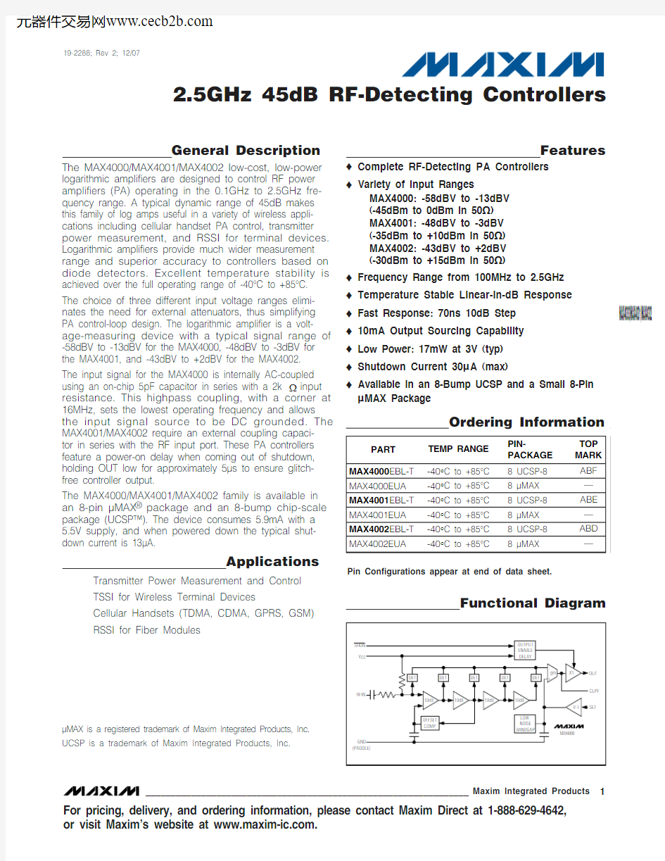
General Description
The MAX4000/MAX4001/MAX4002 low-cost, low-power logarithmic amplifiers are designed to control RF power amplifiers (PA) operating in the 0.1GHz to 2.5GHz fre-quency range. A typical dynamic range of 45dB makes this family of log amps useful in a variety of wireless appli-cations including cellular handset PA control, transmitter power measurement, and RSSI for terminal devices.Logarithmic amplifiers provide much wider measurement range and superior accuracy to controllers based on diode detectors. Excellent temperature stability is achieved over the full operating range of -40°C to +85°C. The choice of three different input voltage ranges elimi-nates the need for external attenuators, thus simplifying PA control-loop design. The logarithmic amplifier is a volt-age-measuring device with a typical signal range of -58dBV to -13dBV for the MAX4000, -48dBV to -3dBV for the MAX4001, and -43dBV to +2dBV for the MAX4002.The input signal for the MAX4000 is internally AC-coupled using an on-chip 5pF capacitor in series with a 2k Ωinput resistance. This highpass coupling, with a corner at 16MHz, sets the lowest operating frequency and allows the input signal source to be DC grounded. The MAX4001/MAX4002 require an external coupling capaci-tor in series with the RF input port. These PA controllers feature a power-on delay when coming out of shutdown,holding OUT low for approximately 5μs to ensure glitch-free controller output.
The MAX4000/MAX4001/MAX4002 family is available in an 8-pin μMAX ?package and an 8-bump chip-scale package (UCSP?). The device consumes 5.9mA with a 5.5V supply, and when powered down the typical shut-down current is 13μA.
Applications
Transmitter Power Measurement and Control TSSI for Wireless Terminal Devices
Cellular Handsets (TDMA, CDMA, GPRS, GSM)RSSI for Fiber Modules
μMAX is a registered trademark of Maxim Integrated Products, Inc.UCSP is a trademark of Maxim Integrated Products, Inc.
Features
?Complete RF-Detecting PA Controllers
?Variety of Input Ranges
MAX4000: -58dBV to -13dBV (-45dBm to 0dBm in 50Ω)MAX4001: -48dBV to -3dBV (-35dBm to +10dBm in 50Ω)MAX4002: -43dBV to +2dBV (-30dBm to +15dBm in 50Ω)
?Frequency Range from 100MHz to 2.5GHz ?Temperature Stable Linear-in-dB Response ?Fast Response: 70ns 10dB Step ?10mA Output Sourcing Capability ?Low Power: 17mW at 3V (typ)?Shutdown Current 30μA (max)
?Available in an 8-Bump UCSP and a Small 8-Pin μMAX Package
MAX4000/MAX4001/MAX4002
2.5GHz 45dB RF-Detecting Controllers
________________________________________________________________Maxim Integrated Products 1
19-2288; Rev 2; 12/07
For pricing, delivery, and ordering information, please contact Maxim Direct at 1-888-629-4642,or visit Maxim’s website at https://www.doczj.com/doc/e52880423.html,.
Pin Configurations appear at end of data sheet.
M A X 4000/M A X 4001/M A X 4002
2.5GHz 45dB RF-Detecting Controllers 2_______________________________________________________________________________________
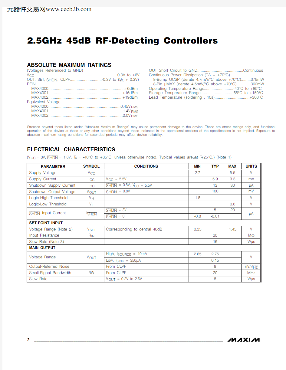
ABSOLUTE MAXIMUM RATINGS
Stresses beyond those listed under “Absolute Maximum Ratings” may cause permanent damage to the device. These are stress ratings only, and functional operation of the device at these or any other conditions beyond those indicated in the operational sections of the specifications is not implied. Exposure to absolute maximum rating conditions for extended periods may affect device reliability.
ELECTRICAL CHARACTERISTICS
(Voltages Referenced to GND)
V CC ...........................................................................-0.3V to +6V OUT, SET, SHDN , CLPF.............................-0.3V to (V CC + 0.3V)RFIN
MAX4000......................................................................+6dBm MAX4001....................................................................+16dBm MAX4002....................................................................+19dBm Equivalent Voltage
MAX4000..................................................................0.45V RMS MAX4001....................................................................1.4V RMS MAX4002....................................................................2.0V RMS
OUT Short Circuit to GND..........................................Continuous Continuous Power Dissipation (TA = +70°C)
8-Bump UCSP (derate 4.7mW/°C above +70°C).........379mW 8-Pin μMAX (derate 4.5mW/°C above +70°C).............362mW Operating Temperature Range ...........................-40°C to +85°C Storage Temperature Range.............................-65°C to +150°C Lead Temperature (soldering , 10s)................................+300°C
MAX4000/MAX4001/MAX4002
2.5GHz 45dB RF-Detecting Controllers
_______________________________________________________________________________________3
Note 1:All devices are 100% production tested at T A = +25°C and are guaranteed by design for T A = -40°C to +85°C as specified.
All production AC testing is done at 100MHz.
Note 2:Typical value only, set-point input voltage range determined by logarithmic slope and logarithmic intercept.
Note 3:Set-point slew rate is the rate at which the reference level voltage, applied to the inverting input of the g m stage, responds to
a voltage step at the SET pin (see Figure 1).
Note 4:Typical min/max range for detector.Note 5:MAX4000 internally AC-coupled.
Note 6:MAX4001/MAX4002 are internally resistive-coupled to V CC .
ELECTRICAL CHARACTERISTICS
(V
= 3V, SHDN = 1.8V, f = 100MHz to 2.5GHz , T = -40°C to +85°C, unless otherwise noted. Typical values are at T = +25°C.)
M A X 4000/M A X 4001/M A X 4002
2.5GHz 45dB RF-Detecting Controllers 4_______________________________________________________________________________________
Typical Operating Characteristics
(V CC = 3V, SHDN = V CC , T A = +25°C, unless otherwise specified. All log conformance plots are normalized to their respective tem-peratures.)
MAX4001 LOG CONFORMANCE vs. INPUT POWER (μMAX)
INPUT POWER (dBm)E R R O R (d B )
10
-30
-20
-10
-3-2-10
1234-4-40
20MAX4002 LOG CONFORMANCE vs. INPUT POWER (μ
MAX)
INPUT POWER (dBm)
E R R O R (d B )
155-25-15-5-3-2-101234
-4
-3525
MAX4000 LOG CONFORMANCE vs. INPUT POWER (μMAX)
INPUT POWER (dBm)E R R O R (d B )
-10
-40
-30
-20
-3-2-101234-4-50
10MAX4002
SET vs. INPUT POWER (UCSP)
INPUT POWER (dBm)
S E T (V )
2010-100-20-300.20.40.60.81.01.21.41.61.8
-40
30
MAX4001
SET vs. INPUT POWER (UCSP)
INPUT POWER (dBm)S E T (V )
100-20-10-30-400.20.40.60.81.01.21.41.61.80
-5020MAX4000
SET vs. INPUT POWER (UCSP)
INPUT POWER (dBm)S E T (V )
-10
-30
-20
-40
-50
0.20.40.60.81.01.21.41.61.80-60
10MAX4002
SET vs. INPUT POWER (μMAX)
INPUT POWER (dBm)
S E T (V )
2010-30-20-1000.40.60.81.01.21.41.61.8
0.2
-4030
MAX4001
SET vs. INPUT POWER (μMAX)
INPUT POWER (dBm)S E T (V )
100-40-30-20-100.40.60.81.01.21.41.61.80.2
-5020MAX4000
SET vs. INPUT POWER (μMAX)
INPUT POWER (dBm)S E T (V )
-10
-50
-40
-30
-20
0.40.60.81.01.21.41.61.80.2-60
10
MAX4000/MAX4001/MAX4002
2.5GHz 45dB RF-Detecting Controllers
_______________________________________________________________________________________5
Typical Operating Characteristics (continued)
(V CC = 3V, SHDN = V CC , T A = +25°C, unless otherwise specified. All log conformance plots are normalized to their respective tem-peratures.)
MAX4002 SET AND LOG CONFORMANCE vs. INPUT POWER AT 0.1GHz (UCSP)
INPUT POWER (dBm)
S E T (V )15
5
-25
-15
-5
0.40.60.81.01.21.41.61.80.2-3
-2-101234-4-35
25
E R R O R (d B
)MAX4001 SET AND LOG CONFORMANCE vs. INPUT POWER AT 0.1GHz (UCSP)
INPUT POWER (dBm)
S E T (V )
10
-30
-20
-10
0.40.60.81.01.21.41.61.80.2-3-2-1
01234-4-40
20
E R R O R (d B )MAX4000 SET AND LOG CONFORMANCE vs. INPUT POWER AT 0.1GHz (UCSP)
INPUT POWER (dBm)
S E T (V )0
-10
-40
-30
-20
0.40.60.81.0
1.21.41.61.80.2-3
-2-101234-4-50
10E R R O R (d B
)
MAX4002 SET AND LOG CONFORMANCE vs. INPUT POWER AT 0.1GHz (μMAX)
INPUT POWER (dBm)
S E T (V )
E R R O R (d B )15
5
-25
-15
-5
0.40.60.81.01.21.41.61.80.2-3
-2-101234-4-35
25
MAX4001 SET AND LOG CONFORMANCE vs. INPUT POWER AT 0.1GHz (μMAX)
INPUT POWER (dBm)
S E T (V )10
-30
-20
-10
0.40.60.81.01.21.41.61.80.2-3
-2-101234-4-40
20
E R R O R (d B )
MAX4000 SET AND LOG CONFORMANCE vs. INPUT POWER AT 0.1GHz (μMAX)
INPUT POWER (dBm)
S E T (V )0
-10
-40
-30
-20
0.40.60.81.01.21.41.61.80.2-3
-2-101234-4-50
10E R R O R (d B )MAX4002 LOG CONFORMANCE vs. INPUT POWER (UCSP)
INPUT POWER (dBm)
E R R O R (d B )
155-25
-15
-5-3-2-101234
-4-35
25
MAX4001 LOG CONFORMANCE vs. INPUT POWER (UCSP)
INPUT POWER (dBm)
E R R O R (d B )
100-30-20-10-3-2-101234-4
-4020
MAX4000 LOG CONFORMANCE vs. INPUT POWER (UCSP)
INPUT POWER (dBm)E R R O R (d B )
-10
-40
-30
-20
-3-2-101234-4-50
10
M A X 4000/M A X 4001/M A X 4002
2.5GHz 45dB RF-Detecting Controllers 6_______________________________________________________________________________________
Typical Operating Characteristics (continued)
(V CC = 3V, SHDN = V CC , T A = +25°C, unless otherwise specified. All log conformance plots are normalized to their respective tem-peratures.)
MAX4002 SET AND LOG CONFORMANCE vs. INPUT POWER AT 1.9GHz (μMAX)
INPUT POWER (dBm)
S E T (V )
E R R O R (d B )15
5
-25
-15
-5
0.40.60.81.01.21.41.61.80.2-3
-2-101234-4-35
25
MAX4001 SET AND LOG CONFORMANCE vs. INPUT POWER AT 1.9GHz (μMAX)
INPUT POWER (dBm)
S E T (V )
E R R O R (d B )10
-30
-20
-10
0.40.60.81.01.21.41.61.80.2-3-2
-101234-4-40
20
MAX4000 SET AND LOG CONFORMANCE vs. INPUT POWER AT 1.9GHz (μ
MAX)
INPUT POWER (dBm)
S E T (V )
E R R O R (d B )0
-10
-40
-30
-20
0.40.60.81.01.21.41.61.80.2-3-2
-101234-4-50
10
MAX4002 SET AND LOG CONFORMANCE vs. INPUT POWER AT 0.9GHz (UCSP)
INPUT POWER (dBm)
S E T (V )15
5
-25
-15
-5
0.40.60.81.01.21.41.61.80.2-3
-2-101234-4-35
25
E R R O R (d B )MAX4001 SET AND LOG CONFORMANCE vs. INPUT POWER AT 0.9GHz (UCSP)
INPUT POWER (dBm)
S E T (V )10
-30
-20
-10
0.40.60.81.01.21.41.61.80.2-3
-2-101234-4-40
20E R R O R (d B )MAX4000 SET AND LOG CONFORMANCE vs. INPUT POWER AT 0.9GHz (UCSP)
INPUT POWER (dBm)
S E T (V )0
-10
-40
-30
-20
0.40.60.81.01.21.41.61.80.2-3
-2-101234-4-50
10E R R O R (d B )MAX4002 SET AND LOG CONFORMANCE vs. INPUT POWER AT 0.9GHz (μMAX)
INPUT POWER (dBm)
S E T (V )
E R R O R (d B )15
5
-25
-15
-5
0.40.60.81.01.21.41.61.80.2-3-2
-101234-4
-35
25
MAX4001 SET AND LOG CONFORMANCE vs. INPUT POWER AT 0.9GHz (μMAX)
INPUT POWER (dBm)
S E T (V )E R R O R (d B )
10
-30
-20
-10
0.40.6
0.81.01.21.41.61.80.2-3-2
-101234-4-40
20
MAX4000 SET AND LOG CONFORMANCE vs. INPUT POWER AT 0.9GHz (μMAX)
INPUT POWER (dBm)
S E T (V )E R R O R (d B )0
-10
-40
-30
-20
0.40.60.81.01.21.41.61.80.2-3-2
-101234-4-50
10
MAX4000/MAX4001/MAX4002
2.5GHz 45dB RF-Detecting Controllers
_______________________________________________________________________________________7
Typical Operating Characteristics (continued)
(V CC = 3V, SHDN = V CC , T A = +25°C, unless otherwise specified. All log conformance plots are normalized to their respective tem-peratures.)
MAX4001 SET AND LOG CONFORMANCE vs. INPUT POWER AT 2.5GHz (UCSP)
INPUT POWER (dBm)
S E T (V )
E R R O R (d B )10
-30
-20
-10
0.40.60.81.01.21.41.61.80.2-3
-2-101234-4-40
20MAX4000 SET AND LOG CONFORMANCE vs. INPUT POWER AT 2.5GHz (UCSP)
INPUT POWER (dBm)
S E T (V )
E R R O R (d B )0
-10
-40
-30
-20
0.40.60.81.01.21.41.61.80.2-3
-2-101234-4-50
10MAX4002 SET AND LOG CONFORMANCE vs. INPUT POWER AT 2.5GHz (μ
MAX)
INPUT POWER (dBm)
S E T (V )E R R O R (d B )15
5
-25
-15
-5
0.40.60.81.01.21.41.61.80.2-3
-2-101234-4-35
25
MAX4001 SET AND LOG CONFORMANCE vs. INPUT POWER AT 2.5GHz (μMAX)
INPUT POWER (dBm)
S E T (V )E R R O R (d B )10
-30
-20
-10
0.40.60.81.01.21.41.61.80.2-3
-2-101234-4-40
20MAX4000 SET AND LOG CONFORMANCE vs. INPUT POWER AT 2.5GHz (
μMAX)
INPUT POWER (dBm)
S E T (V )
E R R O R (d B )
-10
-40
-30
-20
0.40.60.81.01.21.41.61.80.2-3
-2-101234-4-50
10
MAX4002 SET AND LOG CONFORMANCE vs. INPUT POWER AT 1.9GHz (UCSP)
INPUT POWER (dBm)
S E T (V )
E R R O R (d B )15
5-25-15-50.40.6
0.81.01.21.41.61.80.2
-3
-2-101234-4-3525
MAX4001 SET AND LOG CONFORMANCE vs. INPUT POWER AT 1.9GHz (UCSP)
INPUT POWER (dBm)
S E T (V )
E R R O R (d B )10
-30
-20
-10
0.40.6
0.81.01.21.41.61.80.2-3-2
-101234-4-40
20
MAX4000 SET AND LOG CONFORMANCE vs. INPUT POWER AT 1.9GHz (UCSP)
INPUT POWER (dBm)
S E T (V )
E R R O R (d B )0
-10
-40
-30
-20
0.40.60.81.01.21.41.61.80.2-3-2
-101234-4-50
10
MAX4002 SET AND LOG CONFORMANCE vs. INPUT POWER AT 2.5GHz (UCSP)
INPUT POWER (dBm)
S E T (V )E R R O R (d B )15
5
-25
-15
-5
0.40.60.81.01.21.41.61.80.2-3
-2-101234-4-35
25
M A X 4000/M A X 4001/M A X 4002
2.5GHz 45dB RF-Detecting Controllers 8_______________________________________________________________________________________
Typical Operating Characteristics (continued)
(V CC = 3V, SHDN = V CC , T A = +25°C, unless otherwise specified. All log conformance plots are normalized to their respective tem-peratures.)
MAX4002
LOG SLOPE vs. V CC (μMAX)
V CC (V)
L O G S L O P E (m V /d B )
5.0
4.5
4.03.5
3.0
2526
2728293031323334
24
2.5
5.5
MAX4001
LOG SLOPE vs. V CC
(μMAX)
V CC (V)
L O G S L O P E (m V /d B )
5.0
4.5
3.0
3.5
4.025
26272829303132242.5
5.5
MAX4000
LOG SLOPE vs. V CC (
μMAX)
V CC (V)
L O G S L O P E (m V /d B )
5.0
4.5
3.0
3.5
4.02526272829303132242.5
5.5
FREQUENCY (GHz)
L O G S L O P E (m V /d B )
2526272829303132
24
MAX4002
LOG SLOPE vs. FREQUENCY (UCSP)
2.01.51.00.50 2.5
MAX4001
LOG SLOPE vs. FREQUENCY (UCSP)
FREQUENCY (GHz)L O G S L O P E (m V /d B )
252627282930313223
24 2.01.51.00.50 2.5
MAX4000
LOG SLOPE vs. FREQUENCY (UCSP)
FREQUENCY (GHz)
L O G S L O P E (m V /d B )
2.0
1.5
1.0
0.5
2526272829
303124
2.5MAX4002
LOG SLOPE vs. FREQUENCY (μMAX)
FREQUENCY (GHz)
L O G S L O P E (m V /d B )
2.0
1.5
1.0
0.5
25
2627282930313233
24
2.5
MAX4001
LOG SLOPE vs. FREQUENCY (μMAX)
FREQUENCY (GHz)
L O G S L O P E (m V /d B )
2.01.51.00.524252627282930313223
0 2.5
MAX4000
LOG SLOPE vs. FREQUENCY (μMAX)
FREQUENCY (GHz)
L O G S L O P E (m V /d B )
2.0
1.5
1.0
0.5
252627282930
3124
2.5
MAX4000/MAX4001/MAX4002
2.5GHz 45dB RF-Detecting Controllers
_______________________________________________________________________________________9
Typical Operating Characteristics (continued)
(V CC = 3V, SHDN = V CC , T A = +25°C, unless otherwise specified. All log conformance plots are normalized to their respective tem-peratures.)
2.0
1.5
1.00.50
2.5
-44
-42-40-38-36-34-32-46
L O G I N T E R C E P T (d B )
MAX4002
LOG INTERCEPT vs. FREQUENCY (UCSP)
FREQUENCY (GHz)
-50
-48-46-44-42-40-52
2.0
1.5
1.0
0.50 2.5
FREQUENCY (GHz)L O G I N T E R C E P T (d B m )
MAX4001
LOG INTERCEPT vs. FREQUENCY (UCSP)
L O G I N T E R C E P T (d B m )
-60
-59
-58
-57-56-55-61
MAX4000
LOG INTERCEPT vs. FREQUENCY (UCSP)
2.0
1.5
1.0
0.5
2.5FREQUENCY (GHz)MAX4002
LOG INTERCEPT vs. FREQUENCY (μMAX)
FREQUENCY (GHz)
L O G I N T E R C E P T (d B m )
2.01.51.00.5-44-42-40-38-36-34-32-46
0 2.5
MAX4001
LOG INTERCEPT vs. FREQUENCY (μMAX)
FREQUENCY (GHz)
L O G I N T E R C E P T (d B m )
2.0
1.5
1.0
0.5
-48
-47-46-45-44-43-42-41-40-39-49
2.5
MAX4000
LOG INTERCEPT vs. FREQUENCY (μMAX)
FREQUENCY (GHz)
L O G I N T E R C E P T (d B m )
2.0
1.5
1.0
0.5
-58-57-56-55-54-53-52-51-50-59
2.5
L O G S L O P E (m V /d B )
5.0
4.5
4.03.5
3.0
2.5
5.5
25
27
29
3133
23MAX4002
LOG SLOPE vs. V CC (UCSP)
V CC (V)
L O G S L O P E (m V /d B )
25
27
29
3133
23
5.0
4.5
4.03.5
3.0
2.5
5.5
MAX4001
LOG SLOPE vs. V CC (UCSP)
V CC
(V)
L O G S L O P E (m V /d B )
MAX4000
LOG SLOPE vs. V CC (UCSP)
5.04.5
4.03.5
3.0
2.5
5.5
252627282930313224V CC (V)
M A X 4000/M A X 4001/M A X 4002
2.5GHz 45dB RF-Detecting Controllers 10______________________________________________________________________________________
Typical Operating Characteristics (continued)
(V CC = 3V, SHDN = V CC , T A = +25°C, unless otherwise specified. All log conformance plots are normalized to their respective tem-peratures.)
MAX4002 INPUT IMPEDANCE vs. FREQUENCY (μMAX)
FREQUENCY (GHz)
R E S I S T A N C E (Ω)R E A C T A N C E (Ω)
2.0
1.5
1.0
0.5
500
1000
1500
2000
2500
0-400-300-200-1000 -500 -600
-700 -800
2.5
MAX4001 INPUT IMPEDANCE vs. FREQUENCY (μ
MAX)
FREQUENCY (GHz)R E S I S T A N C E (Ω)R E A C T A N C E (Ω)2.0
1.5
1.0
0.5
500
100015002000
2500
0-400-300-200
-1000 -500 -600
-700 -800
2.5
MAX4000 INPUT IMPEDANCE vs. FREQUENCY (μMAX)
FREQUENCY (GHz)
R E S I S T A N C E (Ω)
R E A C T A N C E (Ω)2.0
1.5
1.0
0.5
500
1000150020002500
0-400-300-200
-1000 -500 -600
-700 -800
2.5
5.04.54.03.53.0-44
-42
-40
-38-36-34-46
2.5 5.5
V CC (V)
L O G I N T E R C E P T (d B m )
MAX4002
LOG INTERCEPT vs. V CC
(UCSP)
5.0
4.5
4.03.5
3.0
2.5
5.5-50-48
-46-44-42-40-52
V CC (V)
L O G I N T E R C E P T (d B m )
MAX4001
LOG INTERCEPT vs. V CC (UCSP)
5.0
4.5
4.03.5
3.0
2.5
5.5-60-59-58-57-56-55-61
V CC (V)
L O G I N T E R C E P T (d B m )
MAX4000
LOG INTERCEPT vs. V CC (UCSP)
MAX4002
LOG INTERCEPT vs. V CC (μMAX)
V CC (V)
L O G I N T E R C E P T (d B m )
5.04.54.03.53.0-45
-43-41-39
-37-35-33
-47
2.5 5.5
MAX4001
LOG INTERCEPT vs. V CC (μMAX)
V CC (V)
L O G I N T E R C E P T (d B m )
5.0
4.5
4.03.5
3.0
-48
-46-44-42-40-38-36-502.5
5.5
MAX4000
LOG INTERCEPT vs. V CC (μMAX)
V CC (V)
L O G I N T E R C E P T (d B m )
5.0
4.5
4.03.5
3.0
-59-58-57-56-55-54-53-52-51-50-49-602.5
5.5
MAX4000/MAX4001/MAX4002
2.5GHz 45dB RF-Detecting Controllers
______________________________________________________________________________________11
Typical Operating Characteristics (continued)
(V CC = 3V, SHDN = V CC , T A = +25°C, unless otherwise specified. All log conformance plots are normalized to their respective tem-peratures.)
SUPPLY CURRENT vs. SHDN VOLTAGE
SHDN (V)
S U P P L Y C U R R E N T (m A )
1.81.60.20.40.6 1.0 1.20.8 1.401
23456
7
-1
2.0
SHDN POWER-ON DELAY RESPONSE TIME
2μs/div OUT 500mV/div 1.5V/div
SHDN
5μs
SHDN RESPONSE TIME
M A X 4000 t o c 69
2μs/div
OUT 500mV/div
1.5V/div
SHDN MAX4002 INPUT IMPEDANCE vs. FREQUENCY (UCSP)
FREQUENCY (GHz)
R E S I S T A N C E (Ω)
R E A C T A N C E (Ω)2.0
1.5
1.0
0.5
500
1000
1500
20002500
00
2.5
-400-300-200
-1000-500-600-700
-800-900
-1000MAX4000 INPUT IMPEDANCE vs. FREQUENCY (UCSP)
FREQUENCY (GHz)
R E S I S T A N C E (Ω)
R E A C T A N C E (Ω)
2.0
1.5
1.0
0.5
500
1000
150020002500
0-400-300-200
-1000 -500
-600 -700
-8000
2.5
MAX4001 INPUT IMPEDANCE vs. FREQUENCY (UCSP)
FREQUENCY (GHz)
R E S I S T A N C E (Ω)
R E A C T A N C E (Ω)2.0
1.5
1.0
0.5
5001000
1500
2000
2500
0-400-300-200
-1000-500-600-700
-800-900
-1000
2.5
M A X 4000/M A X 4001/M A X 4002
2.5GHz 45dB RF-Detecting Controllers
Pin Description
MAXIMUM OUT VOLTAGE
vs. V CC BY LOAD CURRENT
V CC (V)
O U T V O L T A G E (V )
5.0
4.5
4.03.5
3.0
2.5
3.03.5
4.0
4.5
5.05.5
2.0
2.5
5.5
MAIN OUTPUT NOISE SPECTRAL DENSITY FREQUENCY (Hz)
N O I S E S P E C T R A L D E N S I T Y (n V /H Z )
1k
10k
100k
1M
101100
10M
98765432
Typical Operating Characteristics (continued)
(V CC = 3V, SHDN = V CC , T A = +25°C, unless otherwise specified. All log conformance plots are normalized to their respective tem-peratures.)
Block Diagram
MAX4000/MAX4001/MAX4002
2.5GHz 45dB RF-Detecting Controllers
______________________________________________________________________________________
13
Detailed Description
The MAX4000/MAX4001/MAX4002 family of logarithmic amplifiers (log amps) is comprised of four main amplifi-er/limiter stages each with a small-signal gain of 10dB.The output stage of each amplifier is applied to a full-wave rectifier (detector). A detector stage also pre-cedes the first gain stage. In total, five detectors each separated by 10dB, comprise the log amp strip. Figure 1 shows the functional diagram of the log amps.
A portion of the PA output power is coupled to RFIN of the log amp controller, and is applied to the log amp strip. Each detector cell outputs a rectified current and all cell currents are summed and form a logarithmic output. The detected output is applied to a high-gain g m stage, which is buffered and then applied to OUT.OUT is applied to the gain-control pin of the PA to close the control loop. The voltage applied to SET determines the output power of the PA in the control loop. The volt-age applied to SET relates to an input power level determined by the log amp detector characteristics.Extrapolating a straight-line fit of the graph of SET vs.RFIN provides the logarithmic intercept. Logarithmic slope, the amount SET changes for each d
B change of RF input, is generally independent of waveform or ter-mination impedance. The MAX4000/MAX4001/MAX4002 slope at low frequencies is about 25mV/dB.Variance in temperature and supply voltage does not alter the slope significantly as shown in the Typical Operating Characteristics .
The MAX4000/MAX4001/MAX4002 are specifically des-igned for use in PA control applications. In a control loop, the output starts at approximately 2.9V (with sup-ply voltage of 3V) for the minimum input signal and falls to a value close to ground at the maximum input. With a portion of the PA output power coupled to RFIN, apply a voltage to SET and connect OUT to the gain-control pin of the PA to control its output power. An external
capacitor from the CLPF pin to ground sets the band-width of the PA control loop.
Transfer Function
Logarithmic slope and intercept determine the transfer function of the MAX4000/MAX4001/MAX4002 family of log amps. The change in SET voltage per dB change in RF input defines the logarithmic slope. Therefore, a 250mV change at SET results in a 10dB change at RFIN. The Log-Conformance plots (see Typica l Oper-a ting Cha ra cteristics ) show the dynamic range of the log amp family. Dynamic range is the range for which the error remains within a band of ±1dB.
The intercept is defined as the point where the linear response, when extrapolated, intersects the y-axis of the Log-Conformance plot. Using these parameters,the input power can be calculated at any SET voltage level within the specified input range with the following
where SET is the set-point voltage, SLOPE is the loga-rithmic slope (V/dB), RFIN is in either dBm or dBV and IP is the logarithmic intercept point utilizing the same units as RFIN.
Applications Information
Controller Mode
Figure 2 provides a circuit example of the MAX4000/MAX4001/MAX4002 configured as a controller. The MAX4000/MAX4001/MAX4002 require a 2.7V to 5.5V supply voltage. Place a 0.1μF low-ESR, surface-mount ceramic capacitor close to V CC to decouple the supply.Electrically isolate the RF input from other pins (espe-cially SET) to maximize performance at high frequencies (especially at the high-power levels of the MAX4002).The MAX4000 has an internal input-coupling capacitor
M A X 4000/M A X 4001/M A X 4002
2.5GHz 45dB RF-Detecting Controllers 14______________________________________________________________________________________
and does not require external AC-coupling. Achieve 50Ωinput matching by connecting a 50Ωresistor between RFIN and ground. See the Typica l Opera ting Characteristics section for a plot of Input Impedance vs.Frequency. See the Additiona l Input Coupling section for other coupling methods.
The MAX4000/MAX4001/MAX4002 log amps function as both the detector and controller in power-control loops. Use a directional coupler to couple a portion of the PA’s output power to the log amp’s RF input. In applications requiring dual-mode operation where there are two PAs and two directional couplers, passively combine the outputs of the directional couplers before applying to the log amp. Apply a set-point voltage to SET from a controlling source (usually a DAC). OUT,which drives the automatic gain-control pin of the PA,corrects any inequality between the RF input level and the corresponding set-point level. This is valid assum-ing the gain control of the variable gain element is posi-tive, such that increasing OUT voltage increases gain.OUT voltage can range from 150mV to within 250mV of the supply rail while sourcing 10mA. Use a suitable load resistor between OUT and GND for PA control inputs that source current. The Typica l Opera ting Characteristics section has a plot of the sourcing capa-bilities and output swing of OUT.
SHDN and Power-On
The MAX4000/MAX4001/MAX4002 can be placed in shutdown by pulling SHDN to ground. SHDN reduces supply current to typically 13μA. A graph of SHDN Response is included in the Typica l Opera ting Characteristics section. Connect SHDN and V CC together for continuous on-operation.
Power Convention
Expressing power in dBm, decibels above 1mW, is the most common convention in RF systems. Log amp input levels specified in terms of power are a result of following common convention. Note that input power does not refer to power, but rather to input voltage rela-tive to a 50Ωimpedance. Use of dBV, decibels with respect to a 1V RMS sine wave, yields a less ambiguous result. The dBV convention has its own pitfalls in that log amp response is also dependent on waveform. A complex input such as CDMA does not have the exact same output response as the sinusoidal signal. The MAX4000/MAX4001/MAX4002 performance specifica-tions are in both dBV and dBm, with equivalent dBm levels for a 50Ωenvironment. To convert dBV values into dBm in a 50Ωnetwork, add 13dB.
Filter Capacitor and Transient Response
In general, the choice of filter capacitor only partially determines the time-domain response of a PA control loop. However, some simple conventions can be applied to affect transient response. A large filter capacitor, C F , dominates time-domain response, but the loop bandwidth remains a factor of the PA gain-control range. The bandwidth is maximized at power outputs near the center of the PA’s range, and mini-mized at the low and high power levels, where the slope of the gain-control curve is lowest.
A smaller valued C F results in an increased loop band-width inversely proportional to the capacitor value.Inherent phase lag in the PA’s control path, usually caused by parasitics at the OUT pin, ultimately results in the addition of complex poles in the AC loop equa-tion. To avoid this secondary effect, experimentally determine the lowest usable C F for the power amplifier of interest. This requires full consideration to the intrica-cies of the PA control function. The worst-case condi-tion, where the PA output is smallest (gain function is steepest), should be used because the PA control function is typically nonlinear. An additional zero can be added to improve loop dynamics by placing a resis-tor in series with C F . See Figure 3 for the gain and phase response for different C F values.
Additional Input Coupling
There are three common methods for input coupling:broadband resistive, narrowband reactive, and series attenuation. A broadband resistive match is implemented by connecting a resistor to ground at RFIN as shown in Figure 4a. A 50Ωresistor (use other values for different input impedances) in this configuration in parallel with the input impedance of the MAX4000 presents an input
impedance of approximately 50Ω. See the Typical Operating Characteristics for the input impedance plot to determine the required external termination at the fre-quency of interest. The MAX4001/MAX4002 require an additional external coupling capacitor in series with the RF input. As the operating frequency increases over 2GHz, input impedance is reduced, resulting in the need for a larger-valued shunt resistor. Use a Smith Chart for calculating the ideal shunt resistor value.
For high frequencies, use narrowband reactive coupling.This implementation is shown in Figure 4b. The matching components are drawn as reactances since these can be either capacitors or inductors depending on the input impedance at the desired frequency and available stan-dard value components. A Smith Chart is used to obtain the input impedance at the desired frequency and then matching reactive components are chosen. Table 1 pro-vides standard component values at some common fre-quencies for the MAX4001. Note that these inductors must have a high SRF (self-resonant frequency), much higher than the intended frequency of operation to imple-ment this matching scheme.
Device sensitivity is increased by the use of a reactive matching network, because a voltage gain occurs before being applied to RFIN. The associated gain is calculated with the following equation:
where R1 is the source impedance to which the device is being matched, and R2 is the input resistance of the device. The gain is the best-case scenario for a perfect match. However, component tolerance and standard value choice often result in a reduced gain.
Figure 4c demonstrates series attenuation coupling.This method is intended for use in applications where the RF input signal is greater than the input range of the device. The input signal is thus resistively divided by the use of a series resistor connected to the RF source.Since the MAX4000/MAX4001/MAX4002 log amps offer a wide selection of RF input ranges, series attenuation
coupling is not needed for typical applications.
MAX4000/MAX4001/MAX4002
2.5GHz 45dB RF-Detecting Controllers
15
M A X 4000/M A X 4001/M A X 4002
Waveform Considerations
The MAX4000/MAX4001/MAX4002 family of log amps respond to voltage, not power, even though input levels are specified in dBm. It is important to realize that input signals with identical RMS power but unique waveforms results in different log amp outputs.
Differing signal waveforms result in either an upward or downward shift in the logarithmic intercept. However,the logarithmic slope remains the same.
Layout Considerations
As with any RF circuit, the layout of the MAX4000/MAX4001/MAX4002 circuits affects performance. Use a short 50Ωline at the input with multiple ground vias along the length of the line. The input capacitor and resistor should both be placed as close to the IC as possible. V CC should be bypassed as close as possi-ble to the IC with multiple vias connecting the capacitor to the ground plane. It is recommended that good RF components be chosen for the desired operating fre-quency range.Electrically isolate RF input from other pins (especially SET) to maximize perfor-mance at high frequencies (especially at the high power levels of the MAX4002).
UCSP Reliability
The UCSP represents a unique package that greatly reduces board space compared to other packages.UCSP reliability is integrally linked to the user’s assem-bly methods, circuit board material, and usage environ-ment. The user should closely review these areas when considering use of a UCSP. This form factor may not perform equally to a packaged product through tradi-tional mechanical reliability tests. Performance through operating life test and moisture resistance remains uncompromised as it is primarily determined by the wafer fabrication process. Mechanical stress perform-ance is a greater consideration for a UCSP. UCSP sol-der joint contact integrity must be considered since the package is attached through direct solder contact to the user’s PCB. Testing done to characterize the UCSP reliability performance shows that it is capable of per-forming reliably through environmental stresses.Results of environmental stress tests and additional usage data and recommendations are detailed in the UCSP application note, which can be found on Maxim’s website, https://www.doczj.com/doc/e52880423.html,.
2.5GHz 45dB RF-Detecting Controllers 16______________________________________________________________________________________
Pin Configurations
Chip Information
TRANSISTOR COUNT: 358
PROCESS: Bipolar
MAX4000/MAX4001/MAX4002
2.5GHz 45dB RF-Detecting Controllers
______________________________________________________________________________________17
9L U C S P , 3x 3.E P S
Package Information
(The package drawing(s) in this data sheet may not reflect the most current specifications. For the latest package outline information go to https://www.doczj.com/doc/e52880423.html,/packages .)
M A X 4000/M A X 4001/M A X 4002
2.5GHz 45dB RF-Detecting Controllers 18______________________________________________________________________________________
Package Information (continued)
(The package drawing(s) in this data sheet may not reflect the most current specifications. For the latest package outline information go to https://www.doczj.com/doc/e52880423.html,/packages .)
2.5GHz 45dB RF-Detecting Controllers Ma xim ca nnot a ssume responsibility for use of a ny circuitry other tha n circuitry entirely embodied in a Ma xim product. No circuit pa tent licenses a re
implied. Maxim reserves the right to change the circuitry and specifications without notice at any time.
Maxim Integrated Products, 120 San Gabriel Drive, Sunnyvale, CA 94086 408-737-7600 ____________________19
?2007 Maxim Integrated Products
is a registered trademark of Maxim Integrated Products, Inc.
Revision History
MAX4000/MAX4001/MAX4002