General Description
The MAX3372E–MAX3379E and MAX3390E–MAX3393E ±15kV ESD-protected level translators provide the level shifting necessary to allow data transfer in a multivoltage system. Externally applied voltages, V CC and V L , set the logic levels on either side of the device. A low-voltage logic signal present on the V L side of the device appears as a high-voltage logic signal on the V CC side of the device, and vice-versa. The MAX3374E/MAX3375E/MAX3376E/MAX3379E and MAX3390E–MAX3393E unidi-rectional level translators level shift data in one direction (V L →V CC or V CC →V L ) on any single data line. The MAX3372E/MAX3373E and MAX3377E/MAX3378E bidi-rectional level translators utilize a transmission-gate-based design (Figure 2) to allow data translation in either direction (V L ?V CC ) on any single data line. The MAX3372E–MAX3379E and MAX3390E–MAX3393E accept V L from +1.2V to +5.5V and V CC from +1.65V to +5.5V, making them ideal for data transfer between low-voltage ASICs/PLDs and higher voltage systems.
All devices in the MAX3372E –MAX3379E , MAX3390E –MAX3393E family feature a three-state output mode that reduces supply current to less than 1μA, thermal short-circuit protection, and ±15kV ESD protection on the V CC side for greater protection in applications that route sig-nals externally. The MAX3372E /MAX3377E operate at a guaranteed data rate of 230kbps. Slew-rate limiting reduces E MI emissions in all 230kbps devices. The MAX3373E –MAX3376E /MAX3378E /MAX3379E and MAX3390E–MAX3393E operate at a guaranteed data rate of 8Mbps over the entire specified operating voltage range. Within specific voltage domains, higher data rates are possible. (See the Timing Characteristics table.)
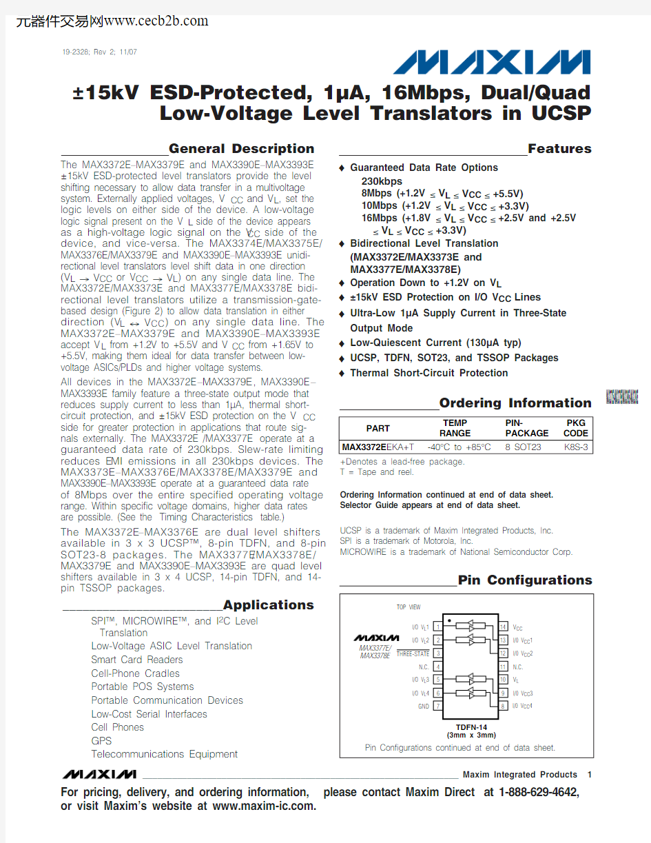
The MAX3372E –MAX3376E are dual level shifters available in 3 x 3 UCSP?, 8-pin TDFN, and 8-pin SOT23-8 packages. The MAX3377E /MAX3378E /MAX3379E and MAX3390E–MAX3393E are quad level shifters available in 3 x 4 UCSP, 14-pin TDFN, and 14-pin TSSOP packages.
________________________Applications
SPI?, MICROWIRE?, and I 2C Level Translation
Low-Voltage ASIC Level Translation Smart Card Readers Cell-Phone Cradles Portable POS Systems
Portable Communication Devices Low-Cost Serial Interfaces Cell Phones GPS
Telecommunications Equipment
Features
?Guaranteed Data Rate Options
230kbps
8Mbps (+1.2V ≤V L ≤V CC ≤+5.5V)10Mbps (+1.2V ≤V L ≤V CC ≤+3.3V)
16Mbps (+1.8V ≤V L ≤V CC ≤+2.5V and +2.5V ≤V L ≤V CC ≤+3.3V)
?Bidirectional Level Translation (MAX3372E/MAX3373E and MAX3377E/MAX3378E)
?Operation Down to +1.2V on V L
?±15kV ESD Protection on I/O V CC Lines ?Ultra-Low 1μA Supply Current in Three-State Output Mode
?Low-Quiescent Current (130μA typ)
?UCSP, TDFN, SOT23, and TSSOP Packages ?Thermal Short-Circuit Protection
MAX3372E–MAX3379E/MAX3390E–MAX3393E
±15kV ESD-Protected, 1μA, 16Mbps, Dual/Quad
Low-Voltage Level Translators in UCSP
________________________________________________________________Maxim Integrated Products
1
19-2328; Rev 2; 11/07
For pricing, delivery, and ordering information,please contact Maxim Direct at 1-888-629-4642,or visit Maxim’s website at https://www.doczj.com/doc/e21429179.html,.
Ordering Information
UCSP is a trademark of Maxim Integrated Products, Inc.SPI is a trademark of Motorola, Inc.
MICROWIRE is a trademark of National Semiconductor Corp.
Ordering Information continued at end of data sheet.Selector Guide appears at end of data sheet.
+Denotes a lead-free package.T = Tape and reel.
M A X 3372E –M A X 3379E /M A X 3390E –M A X 3393E
Low-Voltage Level Translators in UCSP 2_______________________________________________________________________________________
ABSOLUTE MAXIMUM RATINGS
ELECTRICAL CHARACTERISTICS
Stresses beyond those listed under “Absolute Maximum Ratings” may cause permanent damage to the device. These are stress ratings only, and functional operation of the device at these or any other conditions beyond those indicated in the operational sections of the specifications is not implied. Exposure to absolute maximum rating conditions for extended periods may affect device reliability.
(All voltages referenced to GND.)
V CC ...........................................................................-0.3V to +6V I/O V CC_......................................................-0.3V to (V CC + 0.3V)I/O V L_...........................................................-0.3V to (V L + 0.3V)THREE-STATE ...............................................-0.3V to (V L + 0.3V)Short-Circuit Duration I/O V L , I/O V CC to GND...........Continuous Short-Circuit Duration I/O V L or I/O V CC to GND Driven from 40mA Source
(except MAX3372E and MAX3377E).....................Continuous
Continuous Power Dissipation (T A = +70°C)
8-Pin SOT23 (derate 8.9mW/°C above +70°C)...........714mW 8-Pin TDFN (derate 18.2mW/°C above +70°C)........1455mW 3 x 3 UCSP (derate 4.7mW/°C above +70°C)............379mW 3 x 4 UCSP (derate 6.5mW/°C above +70°C)............579mW 14-Pin TSSOP (derate 9.1mW/°C above +70°C)........727mW 14-Pin TDFN (derate 18.2mW/°C above +70°C)......1454mW Operating Temperature Range ...........................-40°C to +85°C Storage Temperature Range.............................-65°C to +150°C Lead Temperature (soldering, 10s).................................+300°C
ELECTRICAL CHARACTERISTICS (continued)
MAX3372E–MAX3379E/MAX3390E–MAX3393E Low-Voltage Level Translators in UCSP
(V CC= +1.65V to +5.5V, V L= +1.2V to (V CC+ 0.3V), GND = 0, I/O V L_and I/O V CC_unconnected, T A= T MIN to T MAX, unless other-
M A X 3372E –M A X 3379E /M A X 3390E –M A X 3393E
Low-Voltage Level Translators in UCSP 4_______________________________________________________________________________________
TIMING CHARACTERISTICS
(V CC = +1.65V to +5.5V, V L = +1.2V to (V CC + 0.3V), GND = 0, R LOAD = 1M Ω, I/O test signal of Figure 1, T A = T MIN to T MAX , unless otherwise noted. Typical values are at V CC = +3.3V, V L = +1.8V, T A = +25°C, unless otherwise noted.) (Notes 1, 2)
MAX3372E–MAX3379E/MAX3390E–MAX3393E
Low-Voltage Level Translators in UCSP
_______________________________________________________________________________________5
and not production tested.
Note 2:For normal operation, ensure V L < (V CC + 0.3V). During power-up, V L > (V CC + 0.3V) will not damage the device. Note 3:To ensure maximum ESD protection, place a 1μF capacitor between V CC and GND. See Applications Circuits .Note 4:10% to 90% Note 5:90% to 10%
TIMING CHARACTERISTICS (continued)
(V = +1.65V to +5.5V, V = +1.2V to (V + 0.3V), GND = 0, R = 1M Ω, I/O test signal of Figure 1, T = T to T , unless
M A X 3372E –M A X 3379E /M A X 3390E –M A X 3393E
Low-Voltage Level Translators in UCSP 6_______________________________________________________________________________________
Typical Operating Characteristics
(R LOAD = 1M Ω, T A = +25°C, unless otherwise noted. All 230kbps TOCs apply to MAX3372E/MAX3377E only. All 8Mbps and 500kbps TOCs apply to MAX3373E–MAX3376E/MAX3378E/MAX3379E and MAX3390E–MAX3393E only.)
V L SUPPLY CURRENT vs. SUPPLY VOLTAGE (DRIVING I/O V L , V CC = +3.3V, V L = +1.8V)
V CC (V)S U P P L Y C U R R E N T (μA )
4.95
4.40
3.85
3.30
2.75
2.20
10020030040050060001.65
5.50V CC SUPPLY CURRENT vs. SUPPLY VOLTAGE (DRIVING I/O V L , V CC = +3.3V, V L = +1.8V)
V CC (V)S U P P L Y C U R R E N T (m A )
4.954.403.853.302.752.200.51.01.52.0
2.5
3.03.50
1.65 5.50
V L SUPPLY CURRENT vs. TEMPERATURE (DRIVING I/O V CC , V CC = +3.3V, V L = +1.8V)
TEMPERATURE (°C)
S U P P L Y C U R R E N T (μA )
6035-151050100150200250300350400
-4085
V CC SUPPLY CURRENT vs. TEMPERATURE
(DRIVING I/O V CC , V CC = +3.3V, V L = +1.8V)
TEMPERATURE (°C)
S U P P L Y C U R R E N T (μA )60
35
-15
10
20040060080010001200140016000-40
85
V L SUPPLY CURRENT vs. CAPACITIVE LOAD (DRIVING I/O V L , V CC = +3.3V, V L
= +1.8V)
CAPACITIVE LOAD (pF)
S U P P L Y C U R R E N T (μA )
85
70
55
40
25
501001502002503003500
10
100
V CC SUPPLY CURRENT vs. CAPACITIVE LOAD (DRIVING I/O V L , V CC = +3.3V, V L = +1.8V)
CAPACITIVE LOAD (pF)
S U P P L Y C U R R E N T (μA )
85
70
55
40
25
500
10001500
20002500
10
100
RISE/FALL TIME vs. CAPACITIVE LOAD (DRIVING I/O V L , V CC = +3.3V, V L = +1.8V)
CAPACITIVE LOAD (pF)
R I S E /F A L L T I M E (n s )
90
80
70
60
50
40
30
500
1000
1500
20002500
020
100
RISE/FALL TIME vs. CAPACITIVE LOAD (DRIVING I/O V L , V CC = +3.3V, V L = +1.8V)
CAPACITIVE LOAD (pF)
R I S E /F A L L T I M E (n s )
45
40
30
35
20
25
15
24
681012141618
010
50
RISE/FALL TIME vs. CAPACITIVE LOAD (DRIVING I/O V L , V CC = +3.3V, V L = +1.8V)
CAPACITIVE LOAD (pF)
R I S E /F A L L T I M E (n s )
45
40
35
30
25
20
15
50
100
150
200250
010
50
MAX3372E–MAX3379E/MAX3390E–MAX3393E
Low-Voltage Level Translators in UCSP
_______________________________________________________________________________________7
PROPAGATION DELAY vs. CAPACITIVE LOAD (DRIVING I/O V L , V CC = +3.3V, V L = +1.8V)
CAPACITIVE LOAD (pF)
P R O P A G A T I O N D E L A Y (n s )
90
80
70
60
50
40
30
100200
300400500600700020
100
PROPAGATION DELAY vs. CAPACITIVE LOAD (DRIVING I/O V L , V CC = +3.3V, V L = +1.8V)
CAPACITIVE LOAD (pF)
P R O P A G A T I O N D E L A Y (n s )
45
40
35
30
25
20
15
3
6
9
12
15
10
50
PROPAGATION DELAY vs. CAPACITIVE LOAD (DRIVING I/O V L , V CC = +3.3V, V L = +1.8V)
CAPACITIVE LOAD (pF)
P R O P A G A T I O N D E L A Y (n s )
45
40
35
30
25
20
15
50
100150200250300010
50
RISE/FALL TIME vs. CAPACITIVE LOAD
(DRIVING I/O V L , V CC = +2.5V, V L = +1.8V)
CAPACITIVE LOAD (pF)
R I S E /F A L L T I M E (n s )
90
80
70
60
50
40
30
500
1000
1500
20002500020
100
RISE/FALL TIME vs. CAPACITIVE LOAD (DRIVING I/O V
L , V CC = +2.5V, V L = +1.8V)
CAPACITIVE LOAD (pF)R I S E /F A L L T I M E (n s )
454035302520152468101214
1050
RISE/FALL TIME vs. CAPACITIVE LOAD (DRIVING I/O V CC , V CC = +2.5V, V L = +1.8V)
CAPACITIVE LOAD (pF)
R I S E /F A L L T I M E (n s )
4540353025201550100150200250300
1050
RISE/FALL TIME vs. CAPACITIVE LOAD (DRIVING I/O V CC , V
CC = +3.3V, V L = +1.8V)
CAPACITIVE LOAD (pF)
R I S E /F A L L T I M E (n s )
90
80
70
60
50
40
30
500
1000
1500
20002500
020
100
RISE/FALL TIME vs. CAPACITIVE LOAD (DRIVING I/O V CC
, V CC = +3.3V, V L = +1.8V)
CAPACITIVE LOAD (pF)
R I S E /F A L L T I M E (n s )
45
40
35
30
25
20
15
2
4681012
010
50
RISE/FALL TIME vs. CAPACITIVE LOAD (DRIVING I/O V CC , V CC = +3.3V, V L = +1.8V)
CAPACITIVE LOAD (pF)
R I S E /F A L L T I M E (n s )
4540353025201550100
1502002503000
1050
Typical Operating Characteristics (continued)
(R LOAD = 1M Ω, T A = +25°C, unless otherwise noted. All 230kbps TOCs apply to MAX3372E/MAX3377E only. All 8Mbps and 500kbps TOCs apply to MAX3373E–MAX3376E/MAX3378E/MAX3379E and MAX3390E–MAX3393E only.)
M A X 3372E –M A X 3379E /M A X 3390E –M A X 3393E
Low-Voltage Level Translators in UCSP 8_______________________________________________________________________________________
Typical Operating Characteristics (continued)
(R LOAD = 1M Ω, T A = +25°C, unless otherwise noted. All 230kbps TOCs apply to MAX3372E/MAX3377E only. All 8Mbps and 500kbps TOCs apply to MAX3373E–MAX3376E/MAX3378E/MAX3379E and MAX3390E–MAX3393E only.)
PROPAGATION DELAY vs. CAPACITIVE LOAD (DRIVING I/O V CC , V CC = +3.3V, V L = +1.8V)
CAPACITIVE LOAD (pF)P R O P A G A T I O N D E L A Y (n s )
90
80
70
60
50
40
30
100200300400500600700020
100
PROPAGATION DELAY vs. CAPACITIVE LOAD (DRIVING I/O V CC , V CC = +3.3V, V L = +1.8V)
CAPACITIVE LOAD (pF)P R O P A G A T I O N D E L A Y (n s )
454035302520151234560
1050
PROPAGATION DELAY vs. CAPACITIVE LOAD (DRIVING I/O V CC , V CC = +3.3V, V L = +1.8V)
CAPACITIVE LOAD (pF)
P R O P A G A T I O N D E L A Y (n s )
4540353025201550100
1502002503000
1050
RISE/FALL TIME vs. CAPACITIVE LOAD (DRIVING I/O V CC , V CC = +2.5V, V L = +1.8V)
CAPACITIVE LOAD (pF)
R I S E /F A L L T I M E (n s )
90
80
70
60
50
40
30
500
1000
1500
20002500
020
100
RISE/FALL TIME vs. CAPACITIVE LOAD (DRIVING I/O V CC , V CC = +2.5V, V L = +1.8V)
CAPACITIVE LOAD (pF)
R I S E /F A L L T I M E (n s )
40
30
20
2
468
1012
10
50
RISE/FALL TIME vs. CAPACITIVE LOAD (DRIVING I/O V CC , V CC = +2.5V, V L = +1.8V)
CAPACITIVE LOAD (pF)
R
I S E /F A L l T I M E (n s )
40
30
20
50100
150200
250300350
10
50
RAIL-TO-RAIL DRIVING
(DRIVING I/O V L , V CC = +3.3V, V L = +1.8V,C LOAD = 50pF, DATA RATE = 230kbps)
M A X 3372E t o c 25
I/O V L_I/O V CC_1V/div 2V/div 1μs/div RAIL-TO-RAIL DRIVING
(DRIVING I/O V L , V CC = +3.3V, V L = +1.8V,C LOAD = 15pF, DATA RATE = 8Mbps)
M A X 3372E t o c 26
I/O V L_I/O V CC_1V/div
2V/div
200ns/div
MAX3372E–MAX3379E/MAX3390E–MAX3393E
Low-Voltage Level Translators in UCSP
_______________________________________________________________________________________9
Typical Operating Characteristics (continued)
(R LOAD = 1M Ω, T A = +25°C, unless otherwise noted. All 230kbps TOCs apply to MAX3372E/MAX3377E only. All 8Mbps and 500kbps TOCs apply to MAX3373E–MAX3376E/MAX3378E/MAX3379E and MAX3390E–MAX3393E only.)
EXITING THREE-STATE OUTPUT MODE (V CC = +3.3V, V L = +1.8V, C LOAD = 50pF)
MAX3372E toc28
I/O V L_
I/O V CC_
2μs/div
THREE-STATE
2V/div
1V/div
1V/div
Pin Description
OPEN-DRAIN DRIVING
(DRIVING I/O V L , V CC = +3.3V, V L = +1.8V,C LOAD = 15pF, DATA RATE = 500kbps)
M A X 3372E t o c 27
I/O V L_I/O V CC_1V/div
2V/div
200ns/div
M A X 3372E –M A X 3379E /M A X 3390E –M A X 3393E
Low-Voltage Level Translators in UCSP 10______________________________________________________________________________________
Detailed Description
The MAX3372E –MAX3379E and MAX3390E –MAX3393E E SD-protected level translators provide the level shifting necessary to allow data transfer in a multivoltage system.Externally applied voltages, V CC and V L , set the logic lev-els on either side of the device. A low-voltage logic signal present on the V L side of the device appears as a high-voltage logic signal on the V CC side of the device, and vice-versa. The MAX3374E /MAX3375E /MAX3376E /MAX3379E and MAX3390E –MAX3393E unidirectional level translators level shift data in one direction (V L →V CC or V CC →V L ) on any single data line. The MAX3372E /MAX3373E and MAX3377E /MAX3378E bidi-rectional level translators utilize a transmission-gate-based design (see Figure 2) to allow data translation in either direction (V L ?V CC ) on any single data line. The MAX3372E –MAX3379E and MAX3390E –MAX3393E
accept V L from +1.2V to +5.5V and V CC from +1.65V to +5.5V, making them ideal for data transfer between low-voltage ASICs/PLDs and higher voltage systems.
All devices in the MAX3372E –MAX3379E , MAX3390E –MAX3393E family feature a three-state output mode that reduces supply current to less than 1μA, thermal short-circuit protection, and ±15kV ESD protection on the V CC side for greater protection in applications that route sig-nals externally. The MAX3372E /MAX3377E operate at a guaranteed data rate of 230kbps. Slew-rate limiting reduces E MI emissions in all 230kbps devices. The MAX3373E –MAX3376E /MAX3378E /MAX3379E and MAX3390E–MAX3393E operate at a guaranteed data rate of 8Mbps over the entire specified operating voltage range. Within specific voltage domains, higher data rates are possible. (See the Timing Characteristics table.)
Figure 1a. Rail-to-Rail Driving I/O V L
Figure 1b. Rail-to-Rail Driving I/O V CC
Level Translation For proper operation ensure that +1.65V ≤V CC≤+5.5V, +1.2V ≤V L≤+5.5V, and V L≤(V CC+ 0.3V). During power-up sequencing, V L≥(V CC+ 0.3V) will not damage the device. During power-supply sequenc-ing, when V CC is floating and V L is powering up, a cur-rent may be sourced, yet the device will not latch up. The speed-up circuitry limits the maximum data rate for devices in the MAX3372E–MAX3379E, MAX3390E–MAX3393E family to 16Mbps. The maximum data rate also depends heavily on the load capacitance (see the Typical Operating Characteristics), output impedance of the driver, and the operational voltage range (see the Timing Characteristics table).
Speed-Up Circuitry The MAX3373E–MAX3376E/MAX3378E/MAX3379E and MAX3390E–MAX3393E feature a one-shot generator that decreases the rise time of the output. When triggered, MOSFETs PU1 and PU2 turn on for a short time to pull up I/O V L_and I/O V CC_to their respective supplies (see Figure 2b). This greatly reduces the rise time and propa-gation delay for the low-to-high transition. The scope photo of Rail-to-Rail Driving for 8Mbps Operation in the Typical Operating Characteristics shows the speed-up circuitry in operation.
Rise-Time Accelerators The MAX3373E–MAX3376E/MAX3378E/MAX3379E and the MAX3390E–MAX3393E have internal rise-time accelerators allowing operation up to 16Mbps. The rise-time accelerators are present on both sides of the device and act to speed up the rise time of the input and output of the device, regardless of the direction of the data. The triggering mechanism for these accelera-tors is both level and edge sensitive. To prevent false triggering of the rise-time accelerators, signal fall times of less than 20ns/V are recommended for both the inputs and outputs of the device. Under less noisy con-ditions, longer signal fall times may be acceptable.
Figure 1c. Open-Drain Driving I/O V CC
Figure 1d. Open-Drain Driving I/O V L
MAX3372E–MAX3379E/MAX3390E–MAX3393E Low-Voltage Level Translators in UCSP
______________________________________________________________________________________11
M A X 3372E –M A X 3379E /M A X 3390E –M A X 3393E
Low-Voltage Level Translators in UCSP 12
______________________________________________________________________________________
Three-State Output Mode
Pull THREE-STATE low to place the MAX3372E –MAX3379E and MAX3390E–MAX3393E in three-state out-put mode. Connect THREE-STATE to V L (logic-high) for normal operation. Activating the three-state output mode disconnects the internal 10k Ωpullup resistors on the I/O V CC and I/O V L lines. This forces the I/O lines to a high-impedance state, and decreases the supply current to less than 1μA. The high-impedance I/O lines in three-state output mode allow for use in a multidrop network.When in three-state output mode, do not allow the voltage
at I/O V L_to exceed (V L + 0.3V), or the voltage at I/O V CC_to exceed (V CC + 0.3V).
Thermal Short-Circuit Protection
Thermal overload detection protects the MAX3372E –MAX3379E and MAX3390E–MAX3393E from short-circuit fault conditions. In the event of a short-circuit fault, when the junction temperature (T J ) reaches +152°C, a thermal sensor signals the three-state output mode logic to force the device into three-state output mode. When T J has cooled to +142°C, normal operation resumes.
Figure 2a. Functional Diagram, MAX3372E/MAX3377E (1 I/O line)
Figure 2b. Functional Diagram, MAX3373E/MAX3378E (1 I/O line)
Figure 3a. Human Body ESD Test Model
Figure 3b. Human Body Current Waveform
±15kV ESD Protection As with all Maxim devices, ESD-protection structures are incorporated on all pins to protect against electrostatic discharges encountered during handling and assembly. The I/O V CC lines have extra protection against static electricity. Maxim’s engineers have developed state-of-the-art structures to protect these pins against E SD of ±15kV without damage. The E SD structures withstand high E SD in all states: normal operation, three-state output mode, and powered down. After an ESD event, Maxim’s E versions keep working without latchup, whereas competing products can latch and must be powered down to remove latchup.
ESD protection can be tested in various ways. The I/O V CC lines of this product family are characterized for protection to the following limits:
1)±15kV using the Human Body Model
2)±8kV using the Contact Discharge method specified
in IEC 1000-4-2
3)±10kV using IE C 1000-4-2’s Air-Gap Discharge
method
ESD Test Conditions E SD performance depends on a variety of conditions. Contact Maxim for a reliability report that documents test setup, test methodology, and test results.
Human Body Model Figure 3a shows the Human Body Model and Figure 3b shows the current waveform it generates when dis-charged into a low impedance. This model consists of a 100pF capacitor charged to the ESD voltage of inter-est, which is then discharged into the test device through a 1.5kΩresistor.
IEC 1000-4-2 The IE C 1000-4-2 standard covers E SD testing and performance of finished equipment; it does not specifi-cally refer to integrated circuits. The MAX3372E–MAX3379E and MAX3390E–MAX3393E help to design equipment that meets Level 3 of IEC 1000-4-2, without the need for additional ESD-protection components. The major difference between tests done using the Human Body Model and IE C 1000-4-2 is higher peak current in IE C 1000-4-2, because series resistance is lower in the IE C 1000-4-2 model. Hence, the E SD with-stand voltage measured to IE C 1000-4-2 is generally lower than that measured using the Human Body Model. Figure 4a shows the IEC 1000-4-2 model, and Figure 4b shows the current waveform for the ±8kV, IEC 1000-4-2, Level 4, ESD contact-discharge test.
The air-gap test involves approaching the device with a charged probe. The contact-discharge method con-nects the probe to the device before the probe is energized.
Machine Model The Machine Model for E SD tests all pins using a 200pF storage capacitor and zero discharge resis-tance. Its objective is to emulate the stress caused by contact that occurs with handling and assembly during manufacturing. Of course, all pins require this protec-tion during manufacturing, not just inputs and outputs. Therefore, after PCB assembly, the Machine Model is less relevant to I/O ports.
MAX3372E–MAX3379E/MAX3390E–MAX3393E Low-Voltage Level Translators in UCSP
______________________________________________________________________________________13
M A X 3372E –M A X 3379E /M A X 3390E –M A X 3393E
Applications Information
Power-Supply Decoupling
To reduce ripple and the chance of transmitting incor-rect data, bypass V L and V CC to ground with a 0.1μF capacitor. See the Typical Operating Circuit. To ensure full ±15kV ESD protection, bypass V CC to ground with a 1μF capacitor. Place all capacitors as close to the power-supply inputs as possible.
I 2C Level Translation
The MAX3373E –MAX3376E , MAX3378E /MAX3379E and MAX3390E–MAX3393E level-shift the data present on the I/O lines between +1.2V and +5.5V, making them ideal for level translation between a low-voltage
ASIC and an I 2C device. A typical application involves interfacing a low-voltage microprocessor to a 3V or 5V D/A converter, such as the MAX517.
Push-Pull vs. Open-Drain Driving
All devices in the MAX3372E –MAX3379E and MAX3390E–MAX3393E family may be driven in a push-pull configuration. The MAX3373E –MAX3376E /MAX3378E /MAX3379E and MAX3390E –MAX3393E include internal 10k Ωresistors that pull up I/O V L_and I/O V CC_to their respective power supplies, allowing operation of the I/O lines with open-drain devices. See the Timing Characteristics table for maximum data rates when using open-drain drivers.
Low-Voltage Level Translators in UCSP
Figure 4b. IEC 1000-4-2 ESD Generator Current Waveform
Figure 4a. IEC 1000-4-2 ESD Test Model Typical Operating Circuit
MAX3372E–MAX3379E/MAX3390E–MAX3393E
Low-Voltage Level Translators in UCSP
______________________________________________________________________________________15
Applications Circuits
M A X 3372E –M A X 3379E /M A X 3390E –M A X 3393E
Low-Voltage Level Translators in UCSP 16______________________________________________________________________________________
Applications Circuits (continued)
Applications Circuits (continued)
MAX3372E–MAX3379E/MAX3390E–MAX3393E Low-Voltage Level Translators in UCSP
M A X 3372E –M A X 3379E /M A X 3390E –M A X 3393E
Low-Voltage Level Translators in UCSP
Applications Circuits (continued)
MAX3372E–MAX3379E/MAX3390E–MAX3393E
Low-Voltage Level Translators in UCSP
Applications Circuits (continued)
M A X 3372E –M A X 3379E /M A X 3390E –M A X 3393E
Low-Voltage Level Translators in UCSP 20
______________________________________________________________________________________
Selector Guide
*Higher data rates are possible (see the Timing Characteristics table).Ordering Information (continued)
+Denotes a lead-free package.**EP = Exposed pad.T = Tape and reel.