1
2801234fc
Single and Dual Transceivers
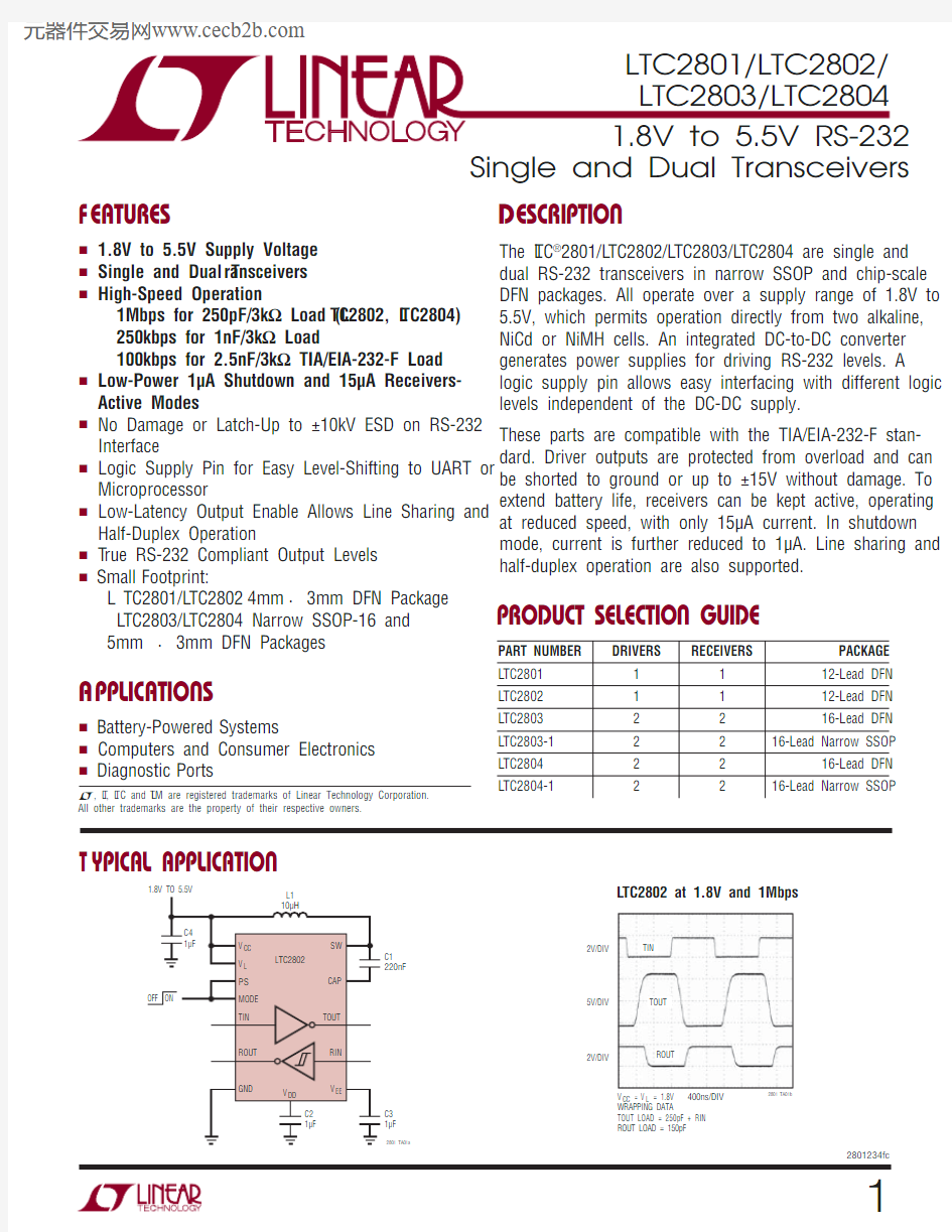
T YPICAL APPLICATION
F EATURES
A PPLICATIONS
D ESCRIPTION The L TC ?2801/L TC2802/L TC2803/L TC2804 are single and
dual RS-232 transceivers in narrow SSOP and chip-scale DFN packages. All operate over a supply range of 1.8V to 5.5V, which permits operation directly from two alkaline, NiCd or NiMH cells. An integrated DC-to-DC converter generates power supplies for driving RS-232 levels. A logic supply pin allows easy interfacing with different logic levels independent of the DC-DC supply.
These parts are compatible with the TIA/EIA-232-F stan-dard. Driver outputs are protected from overload and can be shorted to ground or up to ±15V without damage. To extend battery life, receivers can be kept active, operating at reduced speed, with only 15μA current. In shutdown mode, current is further reduced to 1μA. Line sharing and half-duplex operation are also supported.
n
1.8V to 5.5V Supply Voltage n Single and Dual T ransceivers n High-Speed Operation
1Mbps for 250pF/3kΩ Load (L TC2802, L TC2804) 250kbps for 1nF/3kΩ Load
100kbps for 2.5nF/3kΩ TIA/EIA-232-F Load n Low-Power 1μA Shutdown and 15μA Receivers- Active Modes
n No Damage or Latch-Up to ±10kV ESD on RS-232 Interface
n Logic Supply Pin for Easy Level-Shifting to UART or Microprocessor
n Low-Latency Output Enable Allows Line Sharing and Half-Duplex Operation n T rue RS-232 Compliant Output Levels n Small Footprint:
L TC2801/L TC2802
4mm × 3mm DFN Package L TC2803/L TC2804 Narrow SSOP-16 and
5mm × 3mm DFN Packages
n
Battery-Powered Systems
n Computers and Consumer Electronics n Diagnostic Ports
L , L T , L TC and L TM are registered trademarks of Linear Technology Corporation. All other trademarks are the property of their respective owners.
L TC2802 at 1.8V and 1Mbps
2V/DIV 5V/DIV 2V/DIV
400ns/DIV V CC = V L = 1.8V WRAPPING DATA
TOUT LOAD = 250pF + RIN ROUT LOAD = 150pF
2801 TA01a
PRODUCT SELECTION GUIDE
PART NUMBER DRIVERS
RECEIVERS
PACKAGE L TC28011112-Lead DFN L TC28021112-Lead DFN L TC28032216-Lead DFN
L TC2803-12216-Lead Narrow SSOP
L TC28042216-Lead DFN
L TC2804-1
2
2
16-Lead Narrow SSOP
A BSOLUTE MAXIMUM RATINGS
(Note 1)
Input Supplies
V CC...........................................................–0.3V to 7V V L..........................................................–0.3V to 6.7V Generated Supplies
V DD ................................................V CC –0.3V to 7.5V V EE........................................................0.3V to –7.5V V DD – V EE..............................................................14V SW ..................................................–0.3V to V DD + 0.3V CAP ..................................................+0.3V to V EE – 0.3V TIN, T1IN, T2IN, MODE ................................–0.3V to 7V PS, ON/OFF .....................................–0.3V to (V L + 0.3V) RIN, R1IN, R2IN ..........................................–25V to 25V TOUT, T1OUT, T2OUT .................................–15V to 15V ROUT, R1OUT, R2OUT ....................–0.3V to (V L + 0.3V) Operating Temperature
L TC280XC ................................................0°C to 70°C L TC280XI .............................................–40°C to 85°C Storage Temperature Range ...................–65°C to 125°C Lead Temperature (Soldering, 10 sec)
GN Package ......................................................300°C
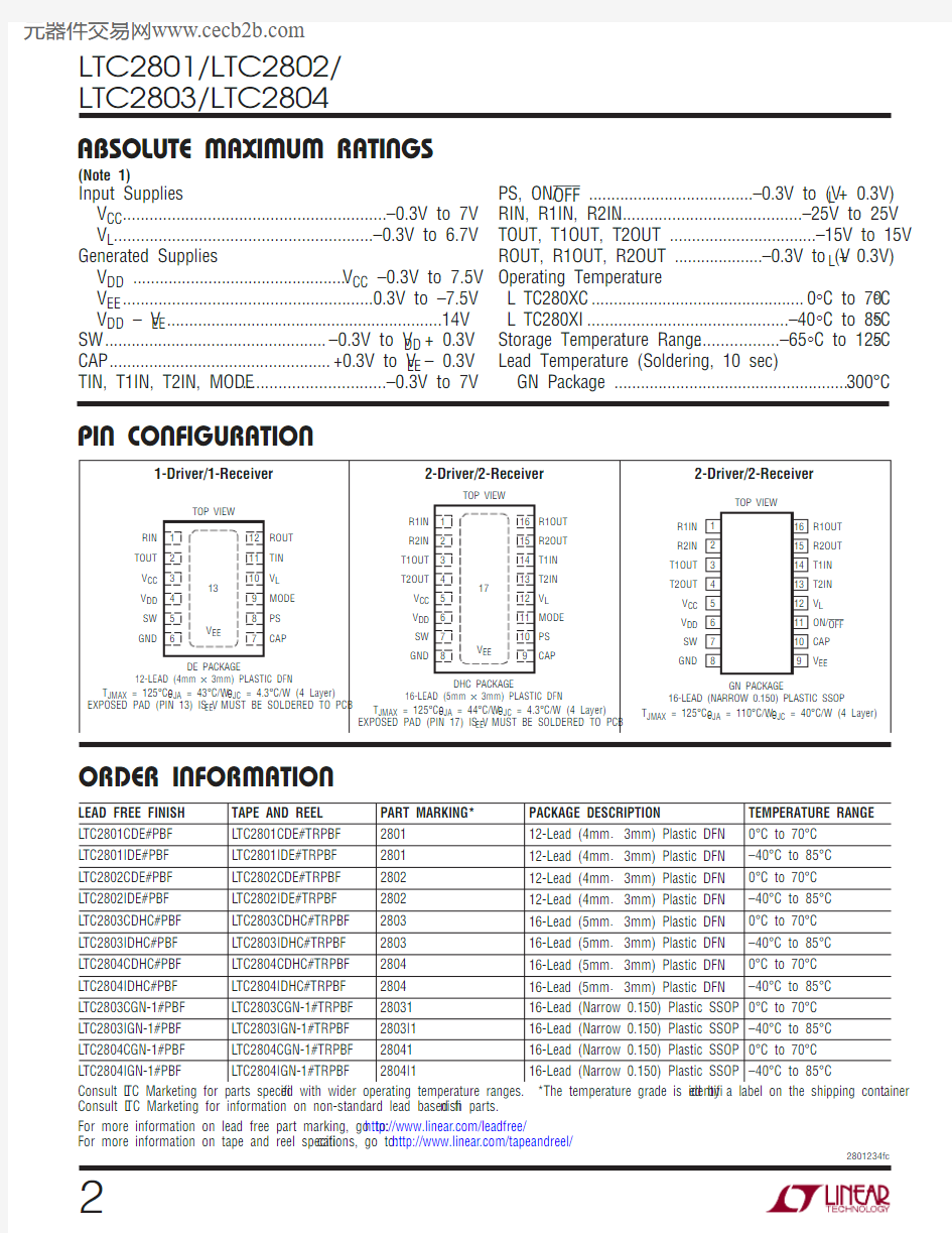
P IN CONFIGURATION
LEAD FREE FINISH TAPE AND REEL PART MARKING*PACKAGE DESCRIPTION TEMPERATURE RANGE
L TC2801CDE#PBF L TC2801CDE#TRPBF280112-Lead (4mm × 3mm) Plastic DFN0°C to 70°C
L TC2801IDE#PBF L TC2801IDE#TRPBF280112-Lead (4mm × 3mm) Plastic DFN–40°C to 85°C
L TC2802CDE#PBF L TC2802CDE#TRPBF280212-Lead (4mm × 3mm) Plastic DFN0°C to 70°C
L TC2802IDE#PBF L TC2802IDE#TRPBF280212-Lead (4mm × 3mm) Plastic DFN–40°C to 85°C
L TC2803CDHC#PBF L TC2803CDHC#TRPBF280316-Lead (5mm × 3mm) Plastic DFN0°C to 70°C
L TC2803IDHC#PBF L TC2803IDHC#TRPBF280316-Lead (5mm × 3mm) Plastic DFN–40°C to 85°C
L TC2804CDHC#PBF L TC2804CDHC#TRPBF280416-Lead (5mm × 3mm) Plastic DFN0°C to 70°C
L TC2804IDHC#PBF L TC2804IDHC#TRPBF280416-Lead (5mm × 3mm) Plastic DFN–40°C to 85°C
L TC2803CGN-1#PBF L TC2803CGN-1#TRPBF2803116-Lead (Narrow 0.150) Plastic SSOP0°C to 70°C
L TC2803IGN-1#PBF L TC2803IGN-1#TRPBF2803I116-Lead (Narrow 0.150) Plastic SSOP–40°C to 85°C
L TC2804CGN-1#PBF L TC2804CGN-1#TRPBF2804116-Lead (Narrow 0.150) Plastic SSOP0°C to 70°C
L TC2804IGN-1#PBF L TC2804IGN-1#TRPBF2804I116-Lead (Narrow 0.150) Plastic SSOP–40°C to 85°C
Consult L TC Marketing for parts speci? ed with wider operating temperature ranges. *The temperature grade is identi? ed by a label on the shipping container. Consult L TC Marketing for information on non-standard lead based ? nish parts.
For more information on lead free part marking, go to: https://www.doczj.com/doc/ea938696.html,/leadfree/
For more information on tape and reel speci? cations, go to: https://www.doczj.com/doc/ea938696.html,/tapeandreel/
ORDER INFORMATION
22801234fc
E LECTRICAL CHARACTERISTICS
The
l denotes the speci? cations which apply over the full operating temperature range, otherwise speci? cations are at T A = 25°C, V CC = 1.8V to 5.5V, V L = 1.8V to 5.5V, Normal Mode. Typical values are given for V CC = V L = 3.3V and T A = 25°C, unless otherwise noted.
SYMBOL PARAMETER CONDITIONS MIN TYP MAX UNITS Power Supplies
I CC V CC Supply Current Outputs Unloaded
Normal Mode (Note 3) Receivers Active Mode Shutdown Mode l
l
2.3
1
1
10
10
mA
μA
μA
I L V L Supply Current Outputs Unloaded
Normal Mode (L TC2801, L TC2802)
Normal Mode (L TC2803, L TC2804)
Receivers Active Mode
Shutdown Mode l
l
l
l
0.08
0.15
15
1
0.15
0.30
30
10
mA
mA
μA
μA
Driver
V OLD Output Voltage R L = 3kΩ Low l–5–5.7V V OHD Output Voltage R L = 3kΩ High l5 6.2V V HYSD Logic Input Hysteresis0.6V I OSD Output Short Circuit Current V L = V CC = 5.5V; V TOUT = 0V l±35±70mA I POLD Power-Off Output Leakage Current V L = V CC = V DD = V EE = 0V; V TOUT = ±2V l±0.1±10μA I OLD Output Leakage Current Shutdown or Receivers Active or
Drivers Disabled Modes, –15V ≤ V TOUT≤ 15V
l±0.1±10μA
Receiver
V IR Input Thresholds Receivers Active Mode l0.8 1.5 2.4V V ILR Input Thresholds Normal Mode, Input Low l0.8 1.3V V IHR Input Thresholds Normal Mode, Input High l 1.7 2.5V V HYSR Input Hysteresis Normal Mode l0.10.4 1.0V V OLR Output Voltage Output Low, I ROUT = 1mA (Sinking)l0.20.4V V OHR Output Voltage Output High, I ROUT = –1mA (Sourcing)l V L –0.4V L –0.2V R IN Input Resistance–15V≤ V RIN≤ 15V l357kΩI OSR Output Short Circuit Current V L = 5.5V; 0V≤ V ROUT≤ V L l±25±50mA Logic
Logic Input Voltage Threshold l0.40.67 ? V L V I IN Logic Input Current l±1μA Power Supply Generator
V DD Regulated V DD Output Voltage Driver R L = 3kΩ (Note 3)
L TC2801, L TC2802: V TIN = V L
L TC2803, L TC2804: V T1IN = V L, V T2IN = 0V
7V
V EE Regulated V EE Output Voltage Driver R L = 3kΩ (Note 3)
L TC2801, L TC2802: V TIN = V L
L TC2803, L TC2804: V T1IN = V L, V T2IN = 0V
–6.3V
32801234fc
4
2801234fc
Note 2: All currents into pins are positive; all voltages are referenced to GND unless otherwise speci? ed.
Note 3: Guaranteed by other measured parameters and not tested directly.Note 4: Time from PS ↑ or ON/OFF ↑ until V DD ≥ 5V and V EE ≤ –5V .
The l denotes the speci? cations which apply over the full operating
temperature range, otherwise speci? cations are at T A = 25°C, V CC = 1.8V to 5.5V, V L = 1.8V to 5.5V, Normal Mode. Typical values are given for V CC = V L = 3.3V and T A = 25°C, unless otherwise noted.
Note 1: Stresses beyond those listed under Absolute Maximum Ratings may cause permanent damage to the device. Exposure to any Absolute Maximum Rating condition for extended periods may affect device reliability and lifetime.
SWITCHING CHARACTERISTICS SYMBOL
PARAMETER CONDITIONS
MIN TYP
MAX
UNITS Maximum Data Rate
L TC2801, L TC2803 (Note 3)
R L = 3k Ω, C L = 2.5nF R L = 3k Ω, C L = 1nF l l 100250kbps kbps L TC2802, L TC2804 (Note 3) R L = 3k Ω, C L = 2.5nF R L = 3k Ω, C L = 1nF R L = 3k Ω, C L = 250pF
l l l
1002501000
kbps kbps kbps
Driver SR(D)
Driver Slew Rate
L TC2801, L TC2803 (Figure 1)
V CC = V L = 1.8V, R L = 3k Ω, C L = 2.5nF V CC = V L = 5.5V, R L = 3k Ω, C L = 50pF l l 4
30
V/μs V/μs L TC2802, L TC2804 (Figure 1)
V CC = V L = 1.8V, R L = 3k Ω, C L = 2.5nF V CC = V L = 5.5V, R L = 3k Ω, C L = 50pF
l l 4
150
V/μs V/μs t PHLD , t PLHD
Driver Propagation Delay
R L = 3k Ω, C L = 50pF (Figure 2) L TC2801, L TC2803 L TC2802, L TC2804l l 10.220.5
μs μs t SKEWD
Driver Skew
R L = 3k Ω, C L = 50pF (Figure 2) L TC2801, L TC2803 L TC2802, L TC280410050ns ns t PZHD , t PZLD Driver Output Enable Time PS = V L , MODE = ↑, R L = 3k Ω, C L = 50pF (Figure 4)
l 0.62μs t PHZD , t PLZD Driver Output Disable Time
PS = V L , MODE = ↓, R L = 3k Ω, C L = 50pF (Figure 4)
l 0.3
2μs
Receiver t PHLR , t PLHR Receiver Propagation Delay C L = 150pF (Figure 3)l 0.20.4μs t SKEWR Receiver Skew
C L = 150pF (Figure 3)50ns t RR , t FR Receiver Rise or Fall Time
C L = 150pF (Figure 3)
l 60200ns t PZHR , t PZLR Shutdown to Receiver Output Enable PS = MODE = ↑ or ON/OFF = ↑, R L = 1k Ω, C L = 150pF (Figure 5)l 515μs t PHZR , t PLZR
Receiver Output Disable upon Shutdown
PS = MODE = ↓ or ON/OFF = ↓, R L = 1k Ω, C L = 150pF (Figure 5)l 0.15
0.3
μs
Power Supply Generator
V DD /V EE Supply Rise Time
(Notes 3 and 4)
l
0.22ms
0V
0V
V OLD
V OHD
TOUT
2801F04
V L
0 OR V L
0V
MODE t r, t f ≤ 40ns
V OHD
V OLD
TOUT
TIN
2801F02
V L
TIN t r, t f ≤ 40ns
TOUT
0V
SR(D) =
6V
t THL or t TLH
Figure 1. Driver Slew Rate Measurement
V OHR
V OLR
t SKEWR = |t PHLR–t PLHR|2801F03
3V
ROUT
–3V
RIN t r, t f ≤ 40ns
Figure 3. Receiver Timing Measurement
V OHD
V OLD
t SKEWD = |t PHLD–t PLHD|2801F02
V L
TOUT
0V
TIN t r, t f ≤ 40ns
Figure 2. Driver Timing Measurement
Figure 4. Driver Enable/Disable Times
TEST CIRCUITS
52801234fc
6
2801234fc
TYPICAL PERFORMANCE CHARACTERISTICS
L TC2803 at 1.8V and 250kbps
L TC2804 at 1.8V and 1Mbps
Drivers Disabled Mode Supply Current vs Supply Voltage
V L
0V
V OLR
V
OHR
ROUT
2801F05
V L –3V OR 3V
0V
PS AND MODE t r , t f ≤ 40ns
Figure 5. Receiver Enable/Disable Times
Supply Current vs Supply Voltage (Dual T ransceiver)
Supply Current vs Data Rate
Supply Current vs Load
Capacitance (Dual T ransceiver)
T A = 25°C, V CC = V L = 3.3V unless otherwise noted.
TEST CIRCUITS
2801 G01
T1IN
T2OUT
T1OUT R2OUT
R1OUT
2V/DIV
10V/DIV
2V/DIV
2μs/DIV V CC
= V L = 1.8V WRAPPING DATA
TOUT LOAD = 1nF + RIN ROUT LOAD = 150pF
2801 G02
T1IN
T2OUT
T1OUT R2OUT
R1OUT 2V/DIV
10V/DIV
2V/DIV 400ns/DIV V CC = V L = 1.8V WRAPPING DATA
TOUT LOAD = 250pF + RIN ROUT LOAD = 150pF
SUPPLY VOLTAGE (V)
6
S U P P L Y C U R R E N T (m A )3.0
2.5
2.01.51.00.50
12
34
2801 G03
5SUPPLY VOLTAGE (V)
1
S U P P L Y C U R R E N T (m A )
605040
3020100
2
3452801 G04
6
DATA RATE (kbps)
S U P P L Y C U R R E N T (
m A )
100
8060
40
20
800
2801 G05
200
400
6001000
100
8060
40
20
LOAD CAPACITANCE (nF)
1
5
2801 G06
234
S U P P L Y C U R R E N T (m A )
7
2801234fc
TYPICAL PERFORMANCE CHARACTERISTICS
Receiver Input Threshold vs Temperature
Receiver Output Voltage vs Load Current
Receiver Output Duty Cycle
Driver Slew Rate vs Load Capacitance
Driver Short-Circuit Current vs Temperature
Shutdown or Drivers Disabled Mode Driver Leakage vs Temperature
Logic Input Threshold vs V L Supply Voltage
L TC2804 Driver Outputs Exiting Shutdown L TC2804 Driver Outputs Enable/Disable
T A = 25°C, V CC = V L = 3.3V unless otherwise noted.
TEMPERATURE (°C)
–50T H R E S H O L D V O L T A G E (V )
3.02.52.01.51.00.50
25752801 GO7–25
50100125
LOAD CURRENT (mA)
O U T P U T V O L T A G E (V )
2801 GO8
6543210
02
451367
8
10
P O S I T I V E D U T Y C Y C L E (%)100
80
60
40
20
100100010000
2801 GO9
DATA RATE (kbps)
LOAD CAPACITANCE (nF)
S L E W R A T E (V /μs )
3
5
2801 G10
1
2
480706050403020100TEMPERATURE (°C)
–50S H O R T -C I R C U I T C U R R E N T (m A )
605040302010
25752801 G11
–25
50100
125
V L SUPPLY VOLTAGE (V)
1T H R E S H O L D V O L T A G E (V )
3.02.52.01.51.0
0.50
2
345
2801 G13
6
L E A K A G E C U R R E N T (A )
10–610–710–810–9
10–10
10–11
2801 G12
TEMPERATURE (°C)
–502575–25
50100125
2V/DIV
5V/DIV
T2OUT
T1OUT
MODE AND PS
V CC = 3.3V
V L = 1.8V
LOAD = 3k + 2.5nF
100μs/DIV 2801 G14
2V/DIV
5V/DIV
T2OUT
T1OUT MODE
V CC = 3.3V
V L = 1.8V
LOAD = 3k + 250nF
2μs/DIV 2801 G15
8
2801234fc
P IN FUNCTIONS MODE CONTROL
PIN NAME PIN NUMBER
COMMENTS 2801
2802280328042803-1
2804-1V CC 355Input Supply (1.8V-5.5V). Bypass to GND with a 1μF capacitor .
V DD 466Generated Positive Supply Voltage for RS-232 Driver (7V). Connect a 1μF capacitor between V DD and GND.
V EE 13*17*9Generated Negative Supply Voltage for RS-232 Driver (–6.3V). Connect a 1μF capacitor between V EE and GND.
SW 577Switch Pin. Connect a 10μH inductor between SW and V CC .GND 688Ground.
CAP 7910Charge Pump Capacitor for Generated Negative Supply Voltage. Connect a 220nF capacitor between CAP and SW .
V L
101212Logic Supply (1.8V-5.5V) for the receiver outputs, driver inputs, and control inputs. This pin should be bypassed to GND with a 220nF capacitor if it’s not tied to V CC .TIN (T1IN, T2IN)1114, 1314, 13Driver Input(s), referenced to V L .TOUT (T1OUT , T2OUT)23, 43, 4RS-232 Driver Output(s).
RIN (R1IN, R2IN)11, 21, 2RS-232 Receiver Input(s). Includes internal 5kΩ termination resistor(s).
ROUT (R1OUT , R2OUT)1216, 1516, 15Receiver Output(s), referenced to V L . Output is short-circuit protected to GND/V CC /V L , and is high impedance in Shutdown mode, allowing data line sharing.
PS 810—Power Supply control pin, referenced to V L . Enables the integrated DC-DC converter .MODE 911—Mode control pin, referenced to V L . See Table 1 for functionality.
ON/OFF
—
—
11
T ransceiver enable pin, referenced to V L . A logic low puts the device in Shutdown mode and places both driver and receiver outputs in a high impedance state.
*Backside thermal pad
Table 1. L TC2801-L TC2804
MODE NAME PS MODE RECEIVER OUTPUT(S)DC-DC DRIVER OUTPUT(S)I VCC *I VL *SHUTDOWN L L HI-Z OFF HI-Z 1μA 1μA RECEIVERS ACTIVE L H ON OFF HI-Z 1μA 15μA DRIVERS DISABLED H L ON ON HI-Z 2.1mA 80μA OR 150μA NORMAL
H
H
ON
ON
ON
2.3mA
80μA OR 150μA
Table 2. L TC2803-1, L TC2804-1
MODE NAME ON/OFF RECEIVER
OUTPUTS DC-DC DRIVER
OUTPUTS I VCC *I VL *SHUTDOWN L HI-Z OFF HI-Z 1μA 1μA NORMAL
H
ON
ON
ON
2.3mA
150μA
*Typical currents for static drivers. Normal mode currents are for unloaded outputs.
9
2801234fc
B LOCK DIAGRAM
LTC2801LTC2802LTC2803LTC2804LTC2803-1LTC2804-1
****
C1L1
1.8V TO 5.5V
1.8V TO 5.5V
FEATURE
2801280228032803-128042804-1DRIVERS and RECEIVERS 1 + 1 1 + 1 2 + 2 2 + 2 2 + 2 2 + 2PACKAGE
DE
DE
DHC
GN
DHC
GN
1.8V - 5.5V OPERATION l l l l l l 1.8V - 5.5V LOGIC SUPPL Y (V L )l l l l l l SHUTDOWN (1μA)l l l l
l l
RECEIVER(S) ACTIVE (15μA)l l l l DRIVER DISABLE
l l l l
100kb/s for R L = 3kΩ, C L = 2.5nF l l l l l l 250kb/s for R L = 3kΩ, C L = 1nF l
l l
l
l l 1Mb/s for R L = 3kΩ, C L = 250pF
l
l
l
FEATURE SUMMARY
10
2801234fc
C1L1
A PPLICATIONS INFORMATION Overview
The L TC2801 family of RS-232 transceivers operates on a V CC supply of 1.8V to 5.5V, utilizing a switching regula-tor to generate the necessary higher voltage rails for the drivers. The transceivers interface with logic operating on any supply from 1.8V to 5.5V, independent of the V CC voltage. Depending on the device, one or two control pins are available to invoke Shutdown, Receiver Active and Driver Disable features.DC-DC Converter
The on-chip DC-DC converter operates from the V CC input, generating a 7V V DD supply and a charge pumped – 6.3V V EE supply, as shown in Figure 6. V DD and V EE power the output stage of the drivers and are regulated to levels that guarantee greater than ±5V output swing. The DC-DC converter requires a 10μH inductor (L1) and a bypass capacitor (C4) of at least 1μF . The recommended size for the charge pump capacitor (C1) is 220nF and for the storage capacitors (C2 and C3) is 1μF . Larger storage capacitors up to 4.7μF may be used if C1 is kept at 20% to 50% their size and C4 is also scaled. Locate C1-C4 close to their associated pins.
Power-Saving Modes
When the DC-DC converter and drivers are turned off (PS or ON/OFF = logic low), V CC supply current is reduced to 1μA. Tables 1 and 2 summarize the modes for each device. In Shutdown mode, V L supply current is reduced to 1μA, and both receiver and driver outputs assume a high im-pedance state.
In Receivers Active mode, the quiescent V L supply current is reduced to 15μA and the driver outputs assume a high impedance state. The receivers operate at a reduced rate (typically 100 kbps) with hysteresis turned off.Half-Duplex Operation
When the DC-DC converter is kept on (PS = logic high), MODE serves as a low-latency driver enable for half-duplex operation. Each driver is enabled and disabled in less than 2μs, while each receiver remains continuously active. This mode of operation is illustrated in Figures 15-17.Battery Operation
To maximize battery life, connect V CC (and L1) directly to the unregulated battery voltage and V L to the regulated supply, as shown in Figure 22. This con? guration typically minimizes conversion loss while providing compatibility with system logic levels.Inductor Selection
A 10μH inductor with a saturation current (I SAT ) rating of at least 200mA and low DCR (copper wire resistance) is recommended. Some small inductors meeting these requirements are listed in Table 3.
Figure 6. DC/DC Converter and Recommended Bypassing
V L Logic Supply
A separate logic supply pin V L allows the L TC2801 family to interface with any logic signal from 1.8V to 5.5V, as shown in Figure 7. Simply connect the desired logic supply to V L . There is no interdependency between V CC and V L ; they may simultaneously operate at any voltage from 1.8V to 5.5V and sequence in any order . If V L is powered separately from V CC , bypass V L with a 220nF capacitor (C5).
Figure 7. V CC and V L
Are Independent
ANY VOLTAGE FROM
ANY VOLTAGE FROM
RS-232
11
2801234fc
Table 3. Recommended Inductors
PART NUMBER
I SAT (mA)MAX DCR (Ω)
SIZE
(mm)
MANUFACTURER
LQH2MCN100K02L 225 1.2 2 × 1.6 × 0.95Murata
https://www.doczj.com/doc/ea938696.html, LBC2016T100K 2450.85 2 × 1.6 × 1.6Taiyo Yuden
https://www.doczj.com/doc/ea938696.html, FSLB2520-100K
220
1.1
2.5 × 2 × 1.6Toko
https://www.doczj.com/doc/ea938696.html,
Capacitor Selection
The small size of ceramic capacitors makes them ideal for the L TC2801 family. X5R and X7R (preferred) types are recommended because their ESR is low and they retain their capacitance over relatively wide voltage and temperature ranges. Use a voltage rating of at least 10V .
Table 4. Recommended Ceramic Capacitor Manufacturers
MANUFACTURER URL
Murata https://www.doczj.com/doc/ea938696.html, TDK https://www.doczj.com/doc/ea938696.html, Taiyo Yuden https://www.doczj.com/doc/ea938696.html, AVX https://www.doczj.com/doc/ea938696.html, Kemet
https://www.doczj.com/doc/ea938696.html,
Inrush Current and Supply Overshoot Precaution In certain applications, such as battery-operated and wall-adapter devices, fast supply slew rates are generated when power is connected. If V CC ’s voltage is greater than 4.5V and its rise time is faster than 10μs, the pins V DD and SW can exceed their ABS MAX values during start-up. When supply voltage is applied to V CC , the voltage difference between V CC and V DD generates inrush current
C1L1
A PPLICATIONS INFORMATION ? owing through inductor L1 and capacitors C1, C2. The peak inrush current must not exceed 2A. To avoid this condition, add a 1Ω resistor as shown in Figure 8. This precaution is not relevant for supply voltages below 4.5V or rise times longer than 10μs.Board Layout
The board layout should minimize the length and area of the SW and CAP traces. Suggested compact layouts for the L TC2801 family are shown in Figure 9 (a) and (b).
Figure 9. Recommended Board Layouts for (a) Single and (b) Dual T ransceiver Parts
Figure 8. Supply Overshoot Protection for Input Supplies of 4.5V or Higher
12
2801234fc
T YPICAL APPLICATIONS Figure 16. Half-Duplex on Single Line Figure 15. Half-Duplex on Single Line, Separate ROUT, TIN
Figure 14. Power-Saving Shutdown Mode
Figure 13. 5V Microprocessor Interface
Figure 12. 1.8V Microprocessor Interface
Figure 11. Cellphone Peripheral Interface
Figure 10. Power-Saving Receivers-Active Mode
Figure 17. Half-Duplex Dual T ransceiver
13
2801234fc
V CC = 5.5V
DRIVERS DISABLED
V CC = 5.5V
DRIVERS LOADED
V CC = 1.8V
DRIVERS DISABLED V CC = 1.8V
DRIVERS LOADED V SW 5V/DIV
200ns/DIV
2801F21
1. NO L1 OR C2-C4 NEEDED.
2. RECEIVERS ACTIVE MODE SHOWN HAS NO DC HYSTERESIS.
3. SEE DUTY CYCLE GRAPH IN TYPICAL PERFORMANCE SECTION.
L
C42μF
L
C L (nF)520.5L TC2803X X L TC2804X X X DATA RATE
(kbps)
100
250
1000
T YPICAL APPLICATIONS Figure 18. Driving Larger Loads
Figure 19. Quad T ransceiver (2.5V < V CC < 5.5V)
Figure 21. Typical SW Pin Waveforms
Figure 20. 100kbps Dual Inverting Level T ranslator (I L = 15μA Static)
14
2801234fc
DHC Package
16-Lead Plastic DFN (5mm × 3mm)
(Reference L TC DWG # 05-08-1706)
T YPICAL APPLICATIONS
NOTE:
1. DRAWING PROPOSED TO BE MADE VARIATION OF VERSION (WJED-1) IN JEDEC PACKAGE OUTLINE MO-229
2. DRAWING NOT TO SCALE
3. ALL DIMENSIONS ARE IN MILLIMETERS
4. DIMENSIONS OF EXPOSED PAD ON BOTTOM OF PACKAGE DO NOT INCLUDE
MOLD FLASH. MOLD FLASH, IF PRESENT, SHALL NOT EXCEED 0.15mm ON ANY SIDE
5. EXPOSED PAD SHALL BE SOLDER PLATED
6. SHADED AREA IS ONLY A REFERENCE FOR PIN 1 LOCATION ON THE
TOP AND BOTTOM OF PACKAGE
BOTTOM VIEW—EXPOSED PAD
RECOMMENDED SOLDER PAD PITCH AND DIMENSIONS
4. DIMENSIONS OF EXPOSED PAD ON BOTTOM OF PACKAGE DO NOT INCLUDE
MOLD FLASH. MOLD FLASH, IF PRESENT, SHALL NOT EXCEED 0.15mm ON ANY SIDE 5. EXPOSED PAD SHALL BE SOLDER PLATED
6. SHADED AREA IS ONLY A REFERENCE FOR PIN 1 LOCATION ON THE TOP AND BOTTOM OF PACKAGE
NOTE:
1. DRAWING PROPOSED TO BE A VARIATION OF VERSION (WGED) IN JEDEC PACKAGE OUTLINE M0-229
2.DRAWING NOT TO SCALE
3. ALL DIMENSIONS ARE IN MILLIMETERS
BOTTOM VIEW—EXPOSED PAD
× 45°RECOMMENDED SOLDER PAD PITCH AND DIMENSIONS APPLY SOLDER MASK TO AREAS THAT ARE NOT SOLDERED
DE/UE Package
12-Lead Plastic DFN (4mm × 3mm)
(Reference L TC DWG # 05-08-1695 Rev D)
15
2801234fc
Information furnished by Linear Technology Corporation is believed to be accurate and reliable. However , no responsibility is assumed for its use. Linear Technology Corporation makes no representa-tion that the interconnection of its circuits as described herein will not infringe on existing patent rights.
P ACKAGE DESCRIPTION
45°
.0532 – .0688TYP .004 – .0098BSC
.254 MIN
RECOMMENDED SOLDER PAD LAYOUT
.0165 ± *DIMENSION DOES NOT INCLUDE MOLD FLASH. MOLD FLASH SHALL NOT EXCEED 0.006" (0.152mm) PER SIDE
**DIMENSION DOES NOT INCLUDE INTERLEAD FLASH. INTERLEAD FLASH SHALL NOT EXCEED 0.010" (0.254mm) PER SIDE
INCHES
(MILLIMETERS)
NOTE:
1. CONTROLLING DIMENSION: INCHES
2. DIMENSIONS ARE IN
3. DRAWING NOT TO SCALE
GN Package
16-Lead Plastic SSOP (Narrow .150 Inch)
(Reference L TC DWG # 05-08-1641)
16
2801234fc
Linear Technology Corporation
1630 McCarthy Blvd., Milpitas, CA 95035-7417
(408) 432-1900 ● FAX: (408) 434-0507 ● www.linear .com
? LINEAR TECHNOLOGY CORPORA TION 2005
LT 0808 REV C ? PRINTED IN USA
C1L1
T YPICAL APPLICATION Figure 22. Diagnostic Port Operating Directly Off Unregulated Battery Voltage
PART NUMBER DESCRIPTION
COMMENTS
L T1780/L T17812-Driver/2-Receiver RS232 T ransceiver Single 5V Supply with 0.1μF Capacitors, 15kV ESD L TC13373-Driver/5-Receiver RS232 T ransceiver Ultralow Power for DTE Applications L TC13385-Driver/3-Receiver RS232 T ransceiver Ultralow Power for DCE Applications
L T1039/L T1039-163-Driver/3-Receiver RS232 T ransceiver 30kΩ Input Impedance for Multi-Drop Applications L TC1348
3-Driver/5-Receiver RS232 T ransceiver
T rue RS232 Levels on 3.3V Supply
RELATED PARTS