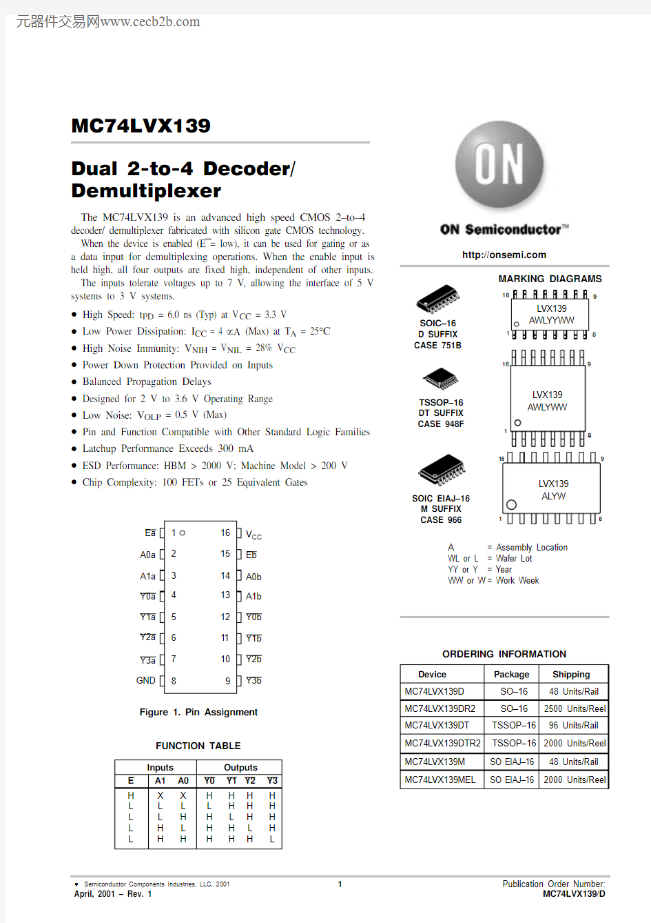
MC74LVX139
Dual 2-to-4 Decoder/ Demultiplexer
The MC74LVX139 is an advanced high speed CMOS 2–to–4 decoder/ demultiplexer fabricated with silicon gate CMOS technology. When the device is enabled (E = low), it can be used for gating or as a data input for demultiplexing operations. When the enable input is held high, all four outputs are fixed high, independent of other inputs. The inputs tolerate voltages up to 7 V, allowing the interface of 5 V systems to 3 V systems.
?High Speed: t PD = 6.0 ns (Typ) at V CC = 3.3 V
?Low Power Dissipation: I CC = 4 μΑ (Max) at T A = 25°C ?High Noise Immunity: V NIH = V NIL = 28% V CC
?Power Down Protection Provided on Inputs
?Balanced Propagation Delays
?Designed for 2 V to 3.6 V Operating Range
?Low Noise: V OLP = 0.5 V (Max)
?Pin and Function Compatible with Other Standard Logic Families ?Latchup Performance Exceeds 300 mA
?ESD Performance: HBM > 2000 V; Machine Model > 200 V ?Chip Complexity: 100 FETs or 25 Equivalent Gates
https://www.doczj.com/doc/d919137591.html,
SOIC–16
D SUFFIX
CASE 751B
MARKING DIAGRAMS
18
9
16
1
8
169
1
169
8
LVX139
AWLYYWW
LVX139
AWLYWW
LVX139
ALYW
TSSOP–16
DT SUFFIX
CASE 948F
SOIC EIAJ–16
M SUFFIX
CASE 966
Device Package Shipping
ORDERING INFORMATION
MC74LVX139D SO–1648 Units/Rail MC74LVX139DR2SO–162500 Units/Reel MC74LVX139DT TSSOP–1696 Units/Rail
TSSOP–162000 Units/Reel MC74LVX139M SO EIAJ–1648 Units/Rail MC74LVX139MEL SO EIAJ–162000 Units/Reel MC74LVX139DTR2
A= Assembly Location
WL or L= Wafer Lot
YY or Y= Year
WW or W= Work Week
ACTIVE–LOW
OUTPUTS
ADDRESS
INPUTS
ACTIVE–LOW
OUTPUTS
ADDRESS
INPUTS
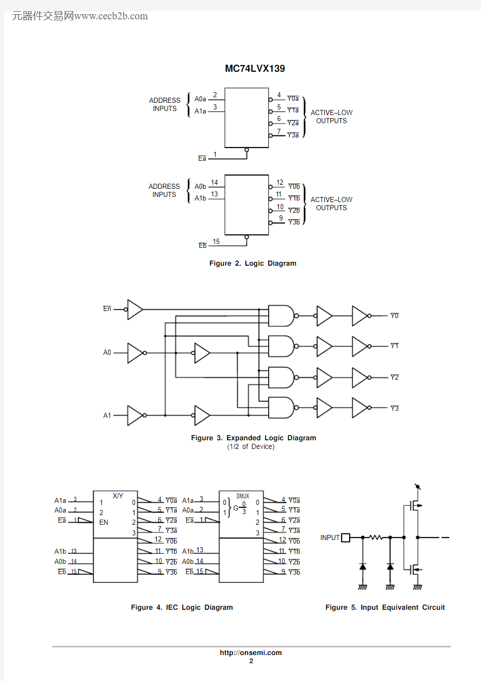
Figure 2. Logic Diagram
En
A0
A1
Y0
Y1
Y2
Y3
Figure 3. Expanded Logic Diagram
(1/2 of Device)
Figure 4. IEC Logic Diagram
Figure 5. Input Equivalent Circuit
MAXIMUM RATINGS (Note 1.)
1.Maximum Ratings are those values beyond which damage to the device may occur. Functional operation should be restricted to the
Recommended Operating Conditions.
2.Tested to EIA/JESD22–A114–A
3.Tested to EIA/JESD22–A115–A
4.Tested to JESD22–C101–A
5.Tested to EIA/JESD78
RECOMMENDED OPERATING CONDITIONS
DC CHARACTERISTICS (Voltages Referenced to GND)
PD
Average operating current can be obtained by the equation: I CC(OPR) = C PD V CC f in + I CC/2 (per decoder). C PD is used to determine the no–load dynamic power consumption; P D = C PD V CC2 f in + I CC V CC.
Figure 6. Switching Waveform
t V CC GND
A V CC
GND
Figure 7. Switching Waveform
*Includes all probe and jig capacitance
Figure 8. Test Circuit
C L *
TEST POINT
D 1
FOR COMPONENTS
2.0 mm × 1.2 mm AND LARGER
OF CAVITY
USER DIRECTION OF FEED
INCLUDING DRAFT AND RADII CONCENTRIC AROUND B 0
7.A 0, B 0, and K 0 are determined by component size. The clearance between the components and the cavity must be within 0.05 mm min to 0.50 mm max. The component cannot rotate more than 10° within the determined cavity
Figure 9. Carrier Tape Specifications
EMBOSSED CARRIER DIMENSIONS (See Notes 8. and 9.)
8.Metric Dimensions Govern–English are in parentheses for reference only.
9.A0, B0, and K0 are determined by component size. The clearance between the components and the cavity must be within 0.05 mm min to
0.50 mm max. The component cannot rotate more than 10° within the determined cavity
Figure 10. Reel Dimensions
REEL DIMENSIONS
HOLE
Figure 11. Reel Winding Direction
DIRECTION OF FEED
Figure 12. Tape Ends for Finished Goods
User Direction of Feed
Figure 13. TSSOP and SOIC R2 Reel Configuration/Orientation TAPE UTILIZATION BY PACKAGE
PACKAGE DIMENSIONS
NOTES:
1.DIMENSIONING AND TOLERANCING PER ANSI Y14.5M, 198
2.
2.CONTROLLING DIMENSION: MILLIMETER.
3.DIMENSIONS A AND B DO NOT INCLUDE MOLD PROTRUSION.
4.MAXIMUM MOLD PROTRUSION 0.15 (0.006)PER SIDE.
5.DIMENSION D DOES NOT INCLUDE DAMBAR PROTRUSION. ALLOWABLE DAMBAR
PROTRUSION SHALL BE 0.127 (0.005) TOTAL IN EXCESS OF THE D DIMENSION AT MAXIMUM MATERIAL CONDITION.
S
B
M
0.25 (0.010)A
S
T DIM MIN MAX MIN MAX INCHES
MILLIMETERS A 9.8010.000.3860.393B 3.80 4.000.1500.157C 1.35 1.750.0540.068D 0.350.490.0140.019F 0.40 1.250.0160.049G 1.27 BSC 0.050 BSC J 0.190.250.0080.009K 0.100.250.0040.009M 0 7 0 7 P 5.80 6.200.2290.244R
0.250.50
0.0100.019
____SOIC–16D SUFFIX CASE 751B–05
ISSUE J
PACKAGE DIMENSIONS
DIM MIN MAX MIN MAX INCHES
MILLIMETERS A 4.90 5.100.1930.200B 4.30 4.500.1690.177C --- 1.20
---0.047
D 0.050.150.0020.006F 0.500.750.0200.030G 0.65 BSC 0.026 BSC H 0.180.280.0070.011J 0.090.200.0040.008J10.090.160.0040.006K 0.190.300.0070.012K10.190.250.0070.010L 6.40 BSC 0.252 BSC M
0 8 0 8 DIMENSIONING AND TOLERANCING PER ANSI Y14.5M, 1982.
CONTROLLING DIMENSION: MILLIMETER.
DIMENSION A DOES NOT INCLUDE MOLD FLASH.PROTRUSIONS OR GATE BURRS. MOLD FLASH OR GATE BURRS SHALL NOT EXCEED 0.15(0.006) PER SIDE.
DIMENSION B DOES NOT INCLUDE INTERLEAD FLASH OR PROTRUSION. INTERLEAD FLASH OR PROTRUSION SHALL NOT EXCEED 0.25 (0.010) PER SIDE.
DIMENSION K DOES NOT INCLUDE DAMBAR PROTRUSION. ALLOWABLE DAMBAR
PROTRUSION SHALL BE 0.08 (0.003) TOTAL IN EXCESS OF THE K DIMENSION AT MAXIMUM MATERIAL CONDITION.
TERMINAL NUMBERS ARE SHOWN FOR REFERENCE ONLY.
DIMENSION A AND B ARE TO BE DETERMINED AT DATUM PLANE -W-.
__
__
16X REF TSSOP–16DT SUFFIX CASE 948F–01ISSUE O
PACKAGE DIMENSIONS
NOTES:
1.DIMENSIONING AND TOLERANCING PER ANSI Y14.5M, 198
2.
SOIC EIAJ–16M SUFFIX CASE 966–01ISSUE O
ON Semiconductor and are trademarks of Semiconductor Components Industries, LLC (SCILLC). SCILLC reserves the right to make changes without further notice to any products herein. SCILLC makes no warranty, representation or guarantee regarding the suitability of its products for any particular purpose, nor does SCILLC assume any liability arising out of the application or use of any product or circuit, and specifically disclaims any and all liability,including without limitation special, consequential or incidental damages. “Typical” parameters which may be provided in SCILLC data sheets and/or specifications can and do vary in different applications and actual performance may vary over time. All operating parameters, including “Typicals” must be validated for each customer application by customer’s technical experts. SCILLC does not convey any license under its patent rights nor the rights of others.SCILLC products are not designed, intended, or authorized for use as components in systems intended for surgical implant into the body, or other applications intended to support or sustain life, or for any other application in which the failure of the SCILLC product could create a situation where personal injury or death may occur. Should Buyer purchase or use SCILLC products for any such unintended or unauthorized application, Buyer shall indemnify and hold SCILLC and its officers, employees, subsidiaries, affiliates, and distributors harmless against all claims, costs, damages, and expenses, and reasonable attorney fees arising out of, directly or indirectly, any claim of personal injury or death associated with such unintended or unauthorized use, even if such claim alleges that SCILLC was negligent regarding the design or manufacture of the part. SCILLC is an Equal Opportunity/Affirmative Action Employer.
PUBLICATION ORDERING INFORMATION
CENTRAL/SOUTH AMERICA:
Spanish Phone :303–308–7143 (Mon–Fri 8:00am to 5:00pm MST)
Email :ONlit–spanish@https://www.doczj.com/doc/d919137591.html,
Toll–Free from Mexico: Dial 01–800–288–2872 for Access –
then Dial 866–297–9322ASIA/PACIFIC : LDC for ON Semiconductor – Asia Support
Phone :1–303–675–2121 (Tue–Fri 9:00am to 1:00pm, Hong Kong Time)
Toll Free from Hong Kong & Singapore:001–800–4422–3781
Email : ONlit–asia@https://www.doczj.com/doc/d919137591.html,
JAPAN : ON Semiconductor, Japan Customer Focus Center
4–32–1 Nishi–Gotanda, Shinagawa–ku, Tokyo, Japan 141–0031Phone : 81–3–5740–2700