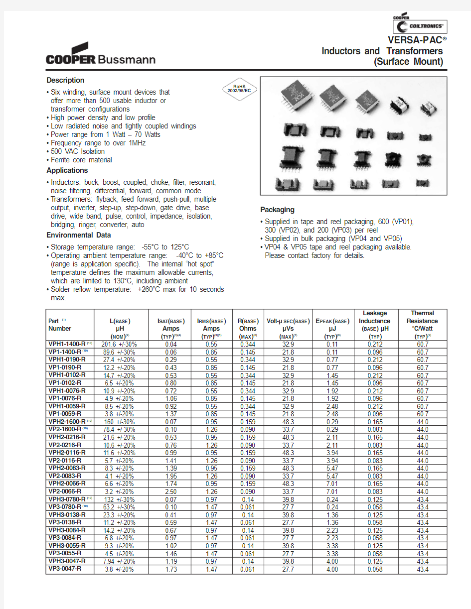
Description
?Six winding, surface mount devices that
offer more than 500 usable inductor or transformer configurations
?High power density and low profile
?Low radiated noise and tightly coupled windings ?Power range from 1 Watt – 70 Watts ?Frequency range to over 1MHz ?500 VAC Isolation ?Ferrite core material Applications
?Inductors:buck, boost, coupled, choke, filter, resonant,noise filtering, differential, forward, common mode ?T ransformers:flyback, feed forward, push-pull, multiple output, inverter, step-up, step-down, gate drive, base drive, wide band, pulse, control, impedance, isolation,bridging, ringer, converter, auto Environmental Data
?Storage temperature range:-55°C to 125°C
?Operating ambient temperature range:-40°C to +85°C (range is application specific).The internal “hot spot”temperature defines the maximum allowable currents,which are limited to 130°C, including ambient
?Solder reflow temperature:+260°C max for 10 seconds max.
Packaging
?Supplied in tape and reel packaging, 600 (VP01), 300 (VP02), and 200 (VP03) per reel
?Supplied in bulk packaging (VP04 and VP05)?VP04 & VP05 tape and reel packaging available.
Please contact factory for details.
RoHS 2002/95/EC
VERSA-PAC temperature rise depends on total power losses and size.Any other PCM configurations other than those suggested could run hotter than acceptable.
Certain topologies or applications must be analyzed for needed requirements and matched with the best VERSA-PAC size and configuration.Proper consideration must be used with all parameters,especially those associated with current rating, energy storage, or maximum volt-seconds.
VERSA-PAC should not be used in off-line or safety related applications.The breakdown voltage from one winding to any other winding is 500 VAC maximum.
PCM
(1)The first three digits in the part number signify the size of the
package.The next four digits specify the A L ,or nanoHenries per turn squared.
(2)L BASE =Nominal Inductance of a single winding.(3)I BASE
is the lessor of I SAT (BASE
)and I RMS (BASE
).
(4)Peak current that will result in 30% saturation of the core.This
current value assumes that equal current flows in all six windings.For applications in which all windings are not simultaneously driven (i.e.flyback, SEPIC, Cuk, etc.), the saturation current per winding may be calculated as follows:
I SAT
=
6x I SAT(BASE)
Number of Windings Driven
(5)RMS Current that results in a surface temperature of approximately
40°C above ambient.The 40°C rise occurs when the specified current flows through each of the six windings.(6)Maximum DC Resistance of each winding.
(7)For multiple windings in series, the volt-μsecond TOT AL
(μVs)
capability varies as the number of windings in series (S):
Volt-μsec TOTAL =S x Volt-μsec (BASE)
For multiple windings in parallel, the volt-μsecond TOTAL
(μVs) capability
is as shown in the table above.
(8)Maximum Energy capability of each winding.This is based on 30%
saturation of the core:
Energy SERIES =S 2
x 1x
0.7L BASE x I 2
SAT(BASE)
Energy PARALLEL =P 2
x
1x
0.7L BASE x I 2
SAT(BASE)
For multiple windings, the energy capability varies as the square of the number of windings.For example, six windings (either parallel or series) can store 36 times more energy than one winding.(9)Thermal Resistance is the approximate surface temperature rise
per Watt of heat loss under still-air conditions.Heat loss is a
combination of core loss and wire loss.The number assumes the underlying PCB copper area equals 150% of the component area.(10)These devices are designed for feed-forward applications, where
load current dominates magnitizing current.
22
Mechanical Diagrams VP2 and VPH2
VP1
and VPH1
TOP VIEW
PIN #1FRONT VIEW
RECOMMENDED PCB LAYOUT
W
87F
NOTES
1) T olerances A - I are ±0.25 mm unless specified otherwise.2) T olerances J - P are +/- 0.1 mm unless specified otherwise.3) Marking as shown
a) Dot for pin #1 identification b) On top of unit:-- VPHx-xxx (product code, size,
4digit part number per family table.)
c) On top of unit:Versa Pac Logo (optional)
d) On bottom of unit:wwllyy =(date code) R = (revision level)
4) All soldering surfaces must be coplanar within 0.102 mm.
A B C D E F G H I J K L M N O P mm mm mm mm mm mm mm mm mm mm mm mm mm mm mm mm max ref max ref ref max ref ref ref ref ref max VP1 and VPH1
12.9
9.2
13.0
0.7
5.9
6.2
1.5
0.1
0.25
11.5
1.5
2.25
9.7
14.2
2.0
0.5
TOP VIEW
R PIN #1FRONT VIEW
RECOMMENDED PCB LAYOUT
W
87F
NOTES
1) T olerances A - I are ±0.25 mm unless specified otherwise.2) T olerances J - P are +/- 0.1 mm unless specified otherwise.3) Marking as shown
a) Dot for pin #1 identification b) On top of unit:-- VPHx-xxx (product code, size,
4digit part number per family table.)
c) On top of unit:Versa Pac Logo (optional)
d) On bottom of unit:wwllyy =(date code) R = (revision level)
4) All soldering surfaces must be coplanar within 0.102 mm.
A B C D E F G H I J K L M N O P mm mm mm mm mm mm mm mm mm mm mm mm mm mm mm mm max ref max ref ref max ref ref ref ref ref max VP2 and VPH2
16.3
12.0
16.8
0.7
6.7
7.8
2.0
0.1
0.30
14.25
1.75
2.5
13.0
18.0
2.5
0.75
Mechanical Diagrams VP4 and VPH4
VP3and VPH3
A B C
D E F G H I J K L M N O mm mm mm mm mm mm mm mm mm mm mm
mm mm mm mm max
ref max ref max ref ref ref ref
ref max
VP3 and VPH317.116.0
22.3
0.7
8.4
3.0
0.1
0.4
14.49 1.79
3.4316.8823.74
2.54
0.75
TOP VIEW
WHITE DOT PIN #1
FRONT VIEW
2
3
1:1:1:1:1:1
D
NOTES
1) T olerances A - I are ±0.25 mm unless specified otherwise.2)T olerances J - P are +/- 0.1 mm unless specified otherwise.3)Marking as shown
a) Dot for pin #1 identification b) On top of unit:-- VPHx-xxx (product code, size,
4digit part number per family table.)
c) On top of unit:Versa Pac Logo (optional)
d) On bottom of unit:wwllyy =(date code) R = (revision level)
4) All soldering surfaces must be coplanar within 0.102 mm.A B C D E F G H I J K L M N O mm mm mm mm mm mm mm mm mm mm mm
mm mm mm mm max
ref max ref max ref ref ref ref
ref max
VP4 and VPH418.018.0
24.6
0.7
10.0
3.3
0.1
0.4
14.25 1.75
3.4319.1426.0
2.5
0.75
TOP VIEW
WHITE DOT PIN #1
FRONT VIEW
2
3
1:1:1:1:1:1
D
NOTES
1) T olerances A - I are ±0.25 mm unless specified otherwise.2) T olerances J - P are +/- 0.1 mm unless specified otherwise.3) Marking as shown
a) Dot for pin #1 identification b) On top of unit:-- VPHx-xxx (product code, size,
4digit part number per family table.)
c) On top of unit:Versa Pac Logo (optional)
d) On bottom of unit:wwllyy =(date code) R = (revision level)
4) All soldering surfaces must be coplanar within 0.102 mm.
Mechanical Diagrams Inductance Characteristics
VP5 and VPH5
A B C D
E F G H I J K L M N O mm mm mm mm mm mm mm mm mm mm mm mm mm mm mm max
ref max ref max ref ref ref ref
ref max VP5 and VPH521.021.0
28.5
0.7
10.8
2.95
0.1
0.4
17.25 2.25
3.15
22.7
29.0
3.0
0.75
TOP VIEW
WHITE DOT PIN #1
6
FRONT VIEW
2
3
1:1:1:1:1:1
D
7
NOTES
1) T olerances A - I are ±0.25 mm unless specified otherwise.2) T olerances J - P are +/- 0.1 mm unless specified otherwise.3) Marking as shown
a) Dot for pin #1 identification b) On top of unit:-- VPHx-xxx (product code, size,
4digit part number per family table.)
c) On top of unit:Versa Pac Logo (optional)
d) On bottom of unit:wwllyy =(date code) R = (revision level)
4) All soldering surfaces must be coplanar within 0.102 mm.
OCL vs.Isat
0.0%
10.0%20.0%30.0%40.0%50.0%60.0%70.0%
80.0%90.0%100.0%0.0%
20.0%40.0%60.0%80.0%100.0%120.0%140.0%160.0%180.0%200.0%
%of Isat
%o f O C L
HOW TO USE MULTIPLE WINDINGS
L TOT AL =L BASE x S 2
=10 μH x 2
2
=40 μH
Where:
L BASE =
Inductance of a single winding
P =Number of windings in parallel (use 1 with all windings in series)S =Number of windings in series
I BASE =
Maximum current rating of one winding
I MAX =I BASE x P
=1 Amp x 1=1Amp L
TOT AL =L BASE x S
2
=10 μH x 12
=10 μH I MAX =I BASE x P =1Amp x 2=2Amps
Series Connected (2 Windings)Parallel Connected (2Windings)
Discrete inductors combine like resistors, when connected in series or parallel.For example, inductors in series add and inductors in parallel reduce in a way similar to Ohm’s Law.
Windings on the same magnetic core behave differently.T wo windings in series result in four times the inductance of a single winding.This is because the inductance varies proportionately to the square of the turns.
Paralleled VERSA-PAC windings result in no change to the net inductance because the total number of turns remains unchanged;only the effective wire size becomes larger.T wo parallel windings result in approximately twice the current carrying capability of a single winding.The net inductance of a given PCM configuration is based on the number of windings in series squared multiplied by the inductance of a single winding (L BASE
).The current rating of a PCM configuration is derived by multiplying the maximum current rating of one winding (I BASE
)by the number of windings in parallel.Examples of simple two-winding devices are shown below:
L Series =L1 + L2 + L3...Ln L Parallel =1/[1/L1 + 1/L2 + 1/L3....1/Ln ]
Each VERSA-P AC can be configured in a variety of ways by simply connecting pins together on the Printed Circuit Board (PCB).As shown below, the connections on the PCB are equal to the pin configuration statement shown at the bottom of the schematic symbol.Connecting a number of windings in parallel will increase the current carrying capability , while connecting in series will multiply the inductance.Each VERSA-P AC part can be configured in at least 6 combinations for inductor use or configured in at least 15 turns ratios for transformer applications.Given 25 VERSA-P AC part numbers, this allows for at least 500 magnetic configurations.The PCM configurations can either be created by the designer or simply chosen from the existing PCM diagrams.The following inductor example shows 6 windings in series, which result in an inductance of 36 times the base
inductance and 1 times the base current.
=36 times the base Inductance from Data Table.
L TOTAL =36 x L BASE
PIN CONFIGURATIONS (2,12)(3,11)(4,10)(5,9)(6,8)
INDUCTOR EXAMPLE
FOR SIZES VP3,VP4 AND VP5
HOW TO PIN-CONFIGURE VERSA-PAC
?
The PCM configurations may be selected from the examples on the following pages or created by the designer.Six PCM inductor and fifteen PCM transformer configurations and equivalent circuit schematics are shown.The printed circuit board layout in each example illustrates the connections to obtain the desired inductance or turns ratio.The examples may be used by the PCB designer to configure VERSA-PAC as desired.
T o assist the designer, VERSA-PAC phasing, coupling and thermal issues have been considered in each of the PCM configurations illustrated.Additionally, the inductance and current ratings, as a function of the respective base values from the following Data T ables, are shown in each PCM example.T urns ratios are also given for each PCM T ransformer shown.It is important to carefully select the proper VERSA-PAC part in order to minimize the component size without exceeding the RMS current capability or saturating the core.The Data T ables indicate maximum ratings.
TRANSFORMER EXAMPLE
FOR SIZES VP3,
VP4 AND VP5
2
L PRIMARY =1x L BASE
I 1:5
PIN CONFIGURATIONS (3,11)(4,10)(5,9)(6,8)
Each VERSA-P AC may be used in at least 15 transformer applications.More than 375 transformer combinations may be achieved using the available 25 VERSA-P AC parts.
5V to 3.3V Buck Converter With 5V Output
This circuit minimizes both board space and cost by eliminating a second regulator.VERSA-P AC ’s gap serves to prevent core
saturation during the switch on-time and also stores energy for the +5V load which is delivered during the flyback interval.The +3.3V buck winding is configured by placing two windings in series while the +5V is generated by an additional flyback winding stacked on the 3.3V output.Extra windings are paralleled with primary
windings to handle more current.The turns ratio of 2:1 adds 1.67V to the +3.3V during the flyback interval to achieve +5V .
12.5A
+
V
V
C
1A
4.2A
3.3V Buck Converter
This circuit utilizes the gap of the VP5-0083 to handle the 12.5Amp output current without saturating.In each of the five VERSA-P AC sizes, the gap is varied to achieve a selection of specific inductance and current values (see VERSA-P AC Data T able).All six windings are connected in parallel to minimize AC/DC copper losses and to maximize heat dissipation.With VERSA-P AC,this circuit works well at or above 300 KHz.Also, the closed flux-path EFD geometry enables much lower radiation
characteristics than open-path bobbin core style components.
LITHIUM-ION BATTERY TO 3.3V SEPIC CONVERTER
The voltage of a Lithium-Ion Battery varies above and below +3.3V depending on the degree of charge.The SEPIC
configuration takes advantage of VERSA-P AC ’s multiple tightly coupled windings.This results in lower ripple current which lowers noise and core losses substantially .The circuit does not require a snubber to control the voltage “spike”associated with switch turn-off,
and is quite efficient due to lower RMS current in the windings.
R
VERSA-PAC VP5-0083
W a t t s
Frequency, kHz
100
0.010.020.0
30.0
40.0
50.060.070.0200
300
400
500
VP 5
VP 4
VP 3
VP 2VP 1
W a t t s
Frequency, kHz
100
0.05.0
10.015.020.0
25.0
30.0
35.040.0200
300
400
500
VP 5
VP 4
VP 3VP 2VP 1
Bipolar (Push-Pull) Power vs Frequency
Unipolar (Flyback) Power vs Frequency
VERSA-P AC ?Performance Characteristics
These curves represent typical power handling capability.
Indicated power levels may not be achievable with all configurations.
Visit us on the Web at https://www.doczj.com/doc/d217263868.html,
1225 Broken Sound Pkwy.Suite F Boca Raton, FL 33487
T el:+1-561-998-4100 T oll Free:+1-888-414-2645 Fax:+1-561-241-6640
This bulletin is intended to present product design solutions and technical information that will help the end user with design applications. Cooper Electronic Technologies reserves the right, without notice, to change design or construction of any products and to discontinue or limit distribution of any products. Cooper Electronic Technologies also reserves the right to change or update, without notice, any technical information contained in this bulletin. Once a product has been selected, it should be tested by the user in all possible applications.
Life Support Policy: Cooper Electronic Technologies does not authorize the use of any of its products for use in life support devices or systems without the express written approval of an officer of the Company.Life support systems are devices which support or sustain life, and whose failure to perform, when properly used in accordance with instructions for use provided in the labeling, can be reasonably expected to result in significant injury to the user.
PM-4301 3/07?Cooper Electronic T echnologies 2007