TECHNICAL DATA
KK 145567
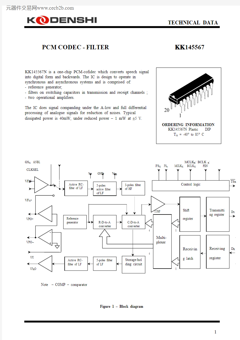
PCM CODEC - FILTER
ORDERING INFORMATION KK 145567N Plastic DIP T A = -40° to 85° C
KK 145567N is a one-chip PCM-cofidec which converts speech signal into digital form and backwards. The IC is design to operate in synchronous and asynchronous systems and is comprised of: - reference generator;
- filters on switching capacitors in transmission and receipt channels ; - two operational amplifiers.
The IC does signal companding under the A-low and full differential processing of analogue signals for reduction of noises. Typical dissipated power is 40mW, under reduced power – 1 mW at ±5 V.
Note – COMP – comparator
Figure 1 – Block diagram
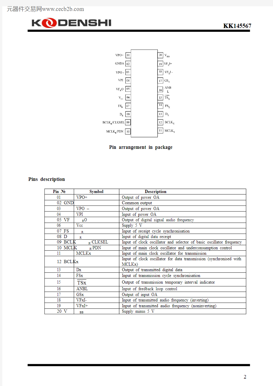
Pins description
Supply source
Characteristics min max Unit
Supply voltage of constant current V CC
V BB
4.75
- 4.75
5.25
- 5.25
V
Consumption power in active mode (without load)
VPI = V BB –
70
60
Consumption power in sleep mode (without load)
VPI = V BB –
5.0
3.0
mW
Digital signal strength
(V CC = 5V ± 5%, V BB = -5V ± 5%, GNDA = 0V)
Dynamic characteristics of digital signals
(V CC = 5V ± 5%, V BB = -5V ± 5%, values of all signals are indicated relatively to GNDA)
Analogue electrical characteristics
(V CC = 5V ± 5%, V BB = -5V ± 5%, VF X I- connected to GS X )
Characteristic min typical
max
Unit Input current (-2.5 V ≤ V in≤ 2.5 V) VF X I+, VF X I-– – ± 0.2 mkA
Input impedance to GNDA at frequency 1 kHz VF X I+, VF X I-10 – MOhm
Input capacitance VF X I+, VF X I-– 10 pF
Input bias voltage GS X Op Amp VF X I+, VF X I-– ± 25 mV
Range of input common-mode voltages VF X I+, VF X I-- 2.5 2.5 V
Amplification ratio without feedback GS X Op Amp
(R load≥ 10 kOhm)
75 – dB
Attenuation factor of in-phase components on out. VF X I+, VF X I-65 dB
Frequency band of unity gain on out. GS X Op Amp
(R load≥ 10 kOhm)
1000 kHz
Equivalent input noise between out. VF X I+, VF X I- and GS X -20 dBm
Load capacitance for GS X Op Amp 0 100 pF
Output range of voltages for GS X R load = 10 kOhm relat. GNDA
R load = 600 Ohm relat. GNDA -
3.5
- 2.8
+ 3.5
+ 2.8
V
Output current (-2.8 V ≤ V out≤ 2.8 V) GS X, VF R O± 5.0 – mA
Output impedance on out. VF R O in the frequency range from 0 to 3.4 kHz 1 Ohm
Load capacitance for output VF R O 0
500
pF Bias voltage for output VF R O relatively to GNDA – ± 100 mV
Noise abatement on supply on transmission
(+) – from 0 to 100 kHz; (-) - from 0 to 100 kHz; 45
45
dB
Analogue transmission characteristics
(V CC = 5 V ± 5%, V BB = -5 V ± 5%, GNDA = 0 V, dBm0 = 1.2276Vrms = 4 dBm with load 600 Ohm, FS X = FS R = 8 kHz, BCLK X = MCLK X = 2.048 MHz at synchronous operation, VF X I- connected to GS X)
Through channel Channel AD Channel DA
Characteristic
min max min max min max
Unit
Change of amplification ratio (relatively to level 0 dBm0 on frequency 1.02 kHz, T A = 25 °С, at
V CC = 5V, V BB = -5V) – – -0.250.25-0.25
0.25 dB
Change of amplification ratio depending on temperature
0 to 70°С
–40 to + 85°С
–
–
–
–
–
–
±0.03
±0.06
–
–
±0.03
±0.06
dB
Change of amplification ratio depending on supply
voltage (V CC = 5V, ± 5%, V BB = 5V ±5%)
– – – ±0.02 – ±0.02 dB
Change of amplification ratio depending on signal strength (relatively to level -10 dBm0 on frequency 1.02 kHz) *
from 3 to –40 dB
from –40 to –50 dB
from –50 to –55 dB
-0.4
-0.8
-1.6
0.4
0.8
1.6
-0.2
-0.4
-0.8
0.2
0.4
0.8
-0.2
-0.4
-0.8
-0.2
-0.4
-0.8
dB
Total distortions of signal at frequency 1 kHz
3 dBм0
0 ÷ - 30 dBm0
-40 dBm0
-45 dBm0
-55 dBm0
33
35
29
24
15
– 33
36
30
25
15
– 33
36
30
25
15
– dB
Total distortions with pseudonoise as per CCITT G.714
-3 dBm0
6 ÷ - 2
7 dBm0
-34 dBm0
-40 dBm0
-55 dBm0
27.5
35
33.1
28.2
13.2
– 28
35.5
33.5
28.5
13.5
– 28.5
36
34.2
30
15
– dB
Noise of "silent" channel (for trough channel and
channel AD psophometrically weighted)
– -70– -70– -83 dBm
Amplitude-frequency characteristic (AFC).
(Relatively to level 0 dBm0 at frequency 1.02 kHz) *
15 Hz
50 Hz
60 Hz
200 Hz
from 300 to 3000 Hz
3300 Hz
3400 Hz
4000 Hz
4600 Hz
–
–
–
–
-0.3
-0.70
-1.6
–
–
-40
-30
-26
–
0.3
0.3
-28
-60
–
–
–
-1.0
-0.15
-0.35
-0.8
–
–
-40
-30
-26
-0.4
0.15
0.15
-14
-32
-0.15
-0.15
-0.15
-0.15
-0.15
-0.35
-0.8
–
–
0.15
0.15
-14
-30
dB
Noise level in the frequency range from 300 to 3000 Hz
(relatively to level 0 dBm0 at frequency 1.02 kHz under
transmission and receipt) *
– -48– -48– -48 dB
Attenuation of parasitic harmonics beyond the limits of gating frequency VFRO VFRO (Relatively to input signal of frequency 300–3400 Hz and level
0 dBm0) from 4600 to 7600 Hz
from 7600 to 8400 Hz
from 8400 to 100000
Hz
–
–
–
-30
-40
-30
–
–
–
–
–
–
–
–
–
-30
-40
-30
dB
continued
Trough channel Channel AD Channel DA
Characteristic
min max min max min max
Unit
Noise of "silent" selected channel (for frequency
8 kHz. Input – GNDA)
– -70– – – -70 dBm Absolute delay (on frequency 1600 Hz) – – – 315– 215 mks Group delay relatively to signal of frequency 1600 Hz
500 ÷ 600 Hz 600 ÷ 800 Hz 800 ÷ 1000 Hz 1000 ÷ 1600 Hz 1600 ÷ 2600 Hz 2600 ÷ 2800 Hz 2800 ÷ 3000 Hz – – – 220
145
75
40
75
105
155
-40
-40
-40
-30
–
–
–
–
–
90
125
175
mks
Crosstalk of signal of frequency 1020 Hz for AD or DA – – – -75– -75 dB Intermodulation distortions of two signals with amplitude
from minus 4 to minus 21 dBm0 for the range 300 ÷ 3400 Hz
– -41– -41– -41 dB * Parameters of the channels А/D and D/А are guaranteed by measuring through channel parameters
Power OA
Characteristic min typical max Unit
Input current (-1 V ≤ VPI ≤ 1V) VPI– – ± 0.5 mkA
Input resistance (-1 V ≤ VPI ≤ 1 V) VPI 5 10 – MOhm Input bias voltage (VPI connected to VPO-) VPI– – ± 50 mV
Output resistance VPO–or VPO+– 1 – Ohm Amplification ratio from VPO– to VPO+ (R load = 300 Ohm, VPO+ to
GNDA, level on VPO– equals 1.77Vrms, 3 dBm0)
– -1 – V/V
Maximum level 0 dBm0 for better than ± 0.1 dB linearity in the range
more than from –10 dBm0 to 3 dBm0 (for R load between VPO+ and VPO)
R load = 600 Ohm R load = 1200 Ohm R load = 10 кOhm 3.3
3.5
4.0
– – Vrms
*
Noise attenuation on supply on Vcc or V BB (VPO- connected to VPI)
VPO–or VPO+ connected to GNDA
dB
0 – 4 kHz 4 – 50 kHz 55 35
Differential noise attenuation on supply on Vcc or V BB (VPO- connected
to VPI), VPO– connected to VPO+ , 0 – 50 kHz 50
dB
Load capacitance (R load≥ 300 Ohm ) VPO+ or VPO– to GNDA0 1000
* dBm0 = 1.2276Vrms = 4 dBm
At Short Frame synchronisation, synchronisation pulses FSx or FS R should have duration equal to duration of clock generator MCLK pulses.
Figure 3 – Time diagram at Short Frame synchronisation
MCLK
R
FSx
BCLK
X
Dx
BCLK
R
FS
R
D
R
At Long Frame synchronisation, synchronisation pulses FSx or FS R should have duration not less than 3 bits of clock generator MCLK.
Figure 4 –Time diagram at Long Frame synchronisation
Package Dimension