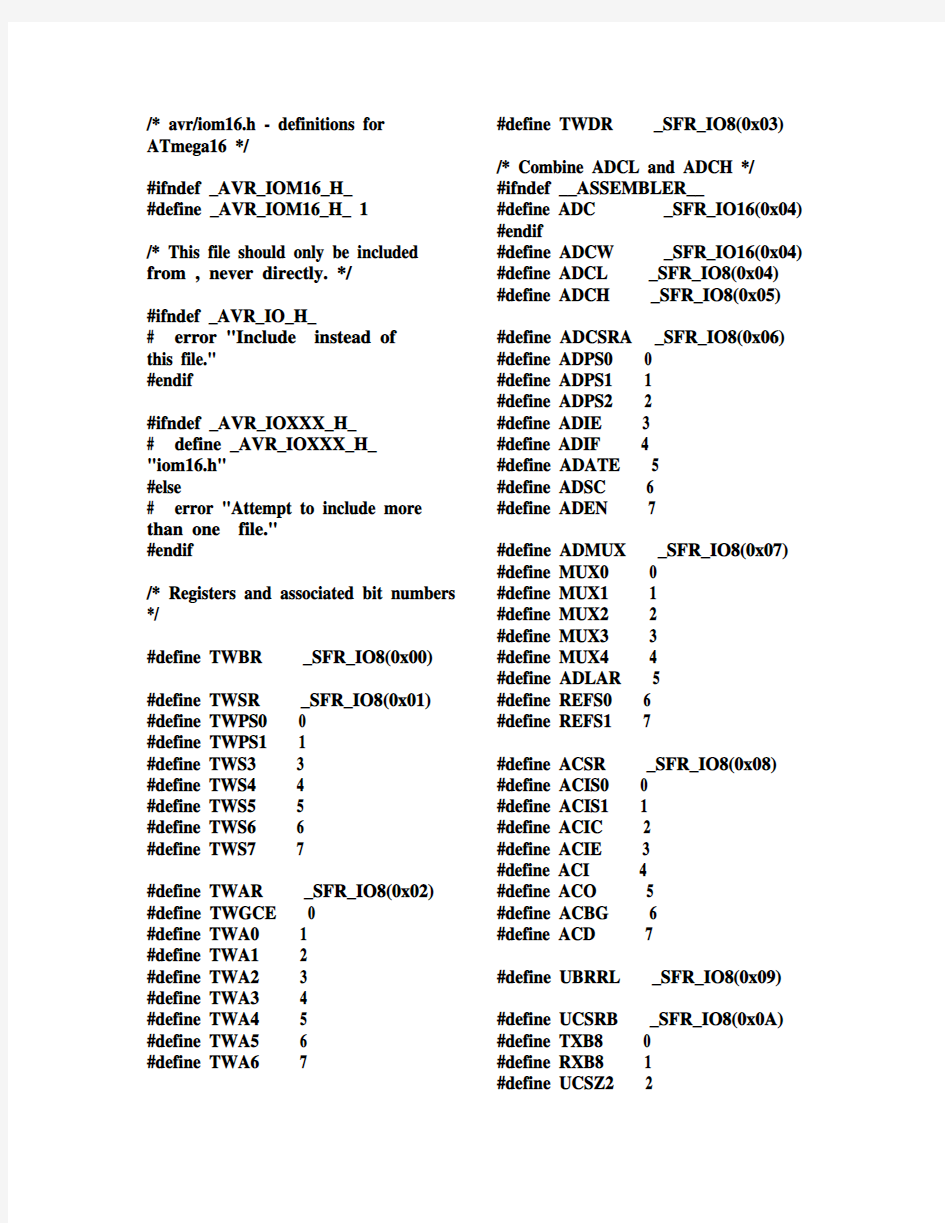
/* avr/iom16.h - definitions for ATmega16 */
#ifndef _AVR_IOM16_H_
#define _AVR_IOM16_H_ 1
/* This file should only be included from
#ifndef _AVR_IO_H_
# error "Include
#endif
#ifndef _AVR_IOXXX_H_
# define _AVR_IOXXX_H_
"iom16.h"
#else
# error "Attempt to include more than one
#endif
/* Registers and associated bit numbers */
#define TWBR _SFR_IO8(0x00)
#define TWSR _SFR_IO8(0x01)
#define TWPS0 0
#define TWPS1 1
#define TWS3 3
#define TWS4 4
#define TWS5 5
#define TWS6 6
#define TWS7 7
#define TWAR _SFR_IO8(0x02) #define TWGCE 0
#define TWA0 1
#define TWA1 2
#define TWA2 3
#define TWA3 4
#define TWA4 5
#define TWA5 6
#define TWA6 7 #define TWDR _SFR_IO8(0x03) /* Combine ADCL and ADCH */
#ifndef __ASSEMBLER__
#define ADC _SFR_IO16(0x04) #endif
#define ADCW _SFR_IO16(0x04) #define ADCL _SFR_IO8(0x04)
#define ADCH _SFR_IO8(0x05) #define ADCSRA _SFR_IO8(0x06) #define ADPS0 0
#define ADPS1 1
#define ADPS2 2
#define ADIE 3
#define ADIF 4
#define ADATE 5
#define ADSC 6
#define ADEN 7
#define ADMUX _SFR_IO8(0x07) #define MUX0 0
#define MUX1 1
#define MUX2 2
#define MUX3 3
#define MUX4 4
#define ADLAR 5
#define REFS0 6
#define REFS1 7
#define ACSR _SFR_IO8(0x08)
#define ACIS0 0
#define ACIS1 1
#define ACIC 2
#define ACIE 3
#define ACI 4
#define ACO 5
#define ACBG 6
#define ACD 7
#define UBRRL _SFR_IO8(0x09) #define UCSRB _SFR_IO8(0x0A) #define TXB8 0
#define RXB8 1
#define UCSZ2 2
#define RXEN 4
#define UDRIE 5
#define TXCIE 6
#define RXCIE 7
#define UCSRA _SFR_IO8(0x0B) #define MPCM 0
#define U2X 1
#define PE 2
#define DOR 3
#define FE 4
#define UDRE 5
#define TXC 6
#define RXC 7
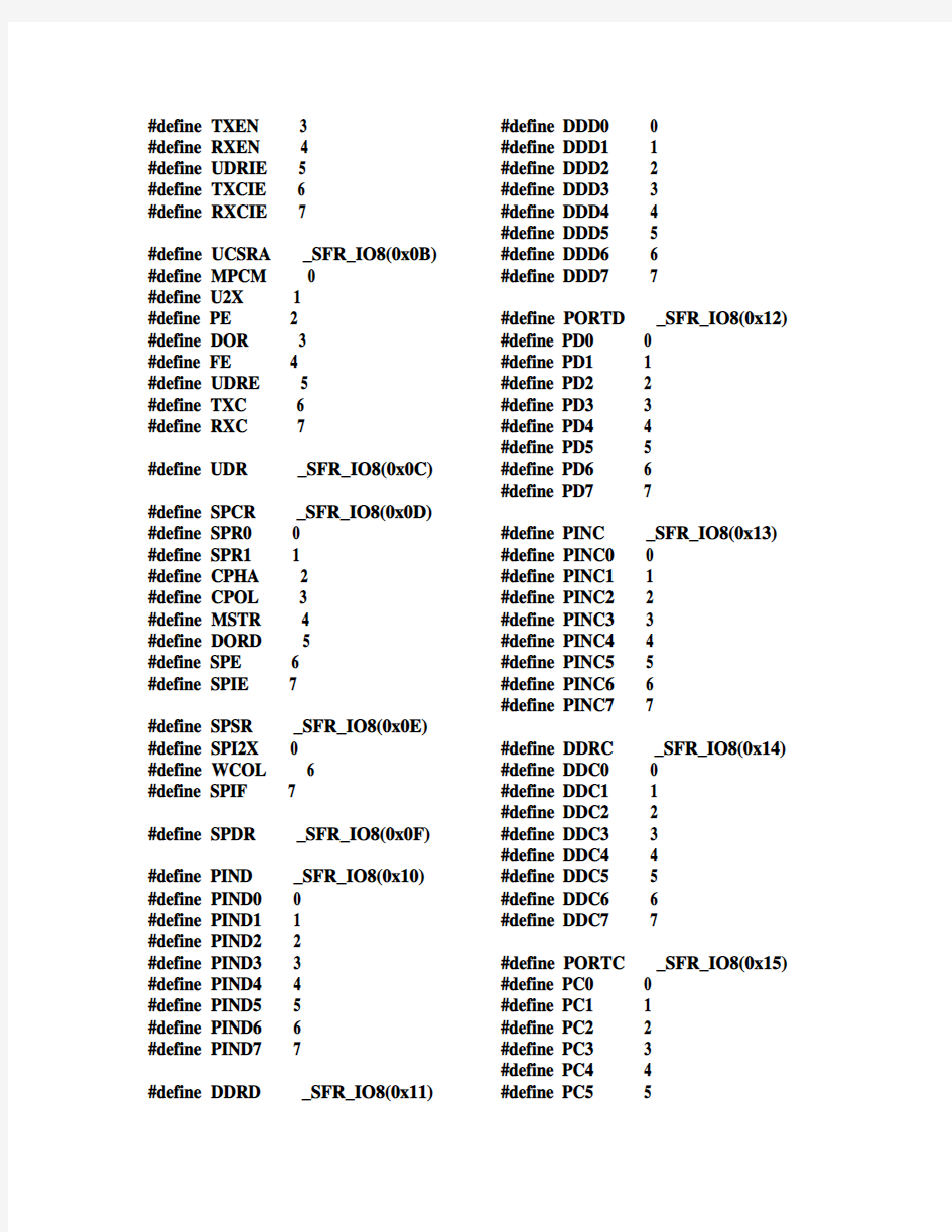
#define UDR _SFR_IO8(0x0C) #define SPCR _SFR_IO8(0x0D) #define SPR0 0
#define SPR1 1
#define CPHA 2
#define CPOL 3
#define MSTR 4
#define DORD 5
#define SPE 6
#define SPIE 7
#define SPSR _SFR_IO8(0x0E) #define SPI2X 0
#define WCOL 6
#define SPIF 7
#define SPDR _SFR_IO8(0x0F) #define PIND _SFR_IO8(0x10) #define PIND0 0
#define PIND1 1
#define PIND2 2
#define PIND3 3
#define PIND4 4
#define PIND5 5
#define PIND6 6
#define PIND7 7
#define DDRD _SFR_IO8(0x11) #define DDD1 1
#define DDD2 2
#define DDD3 3
#define DDD4 4
#define DDD5 5
#define DDD6 6
#define DDD7 7
#define PORTD _SFR_IO8(0x12) #define PD0 0
#define PD1 1
#define PD2 2
#define PD3 3
#define PD4 4
#define PD5 5
#define PD6 6
#define PD7 7
#define PINC _SFR_IO8(0x13) #define PINC0 0
#define PINC1 1
#define PINC2 2
#define PINC3 3
#define PINC4 4
#define PINC5 5
#define PINC6 6
#define PINC7 7
#define DDRC _SFR_IO8(0x14) #define DDC0 0
#define DDC1 1
#define DDC2 2
#define DDC3 3
#define DDC4 4
#define DDC5 5
#define DDC6 6
#define DDC7 7
#define PORTC _SFR_IO8(0x15) #define PC0 0
#define PC1 1
#define PC2 2
#define PC3 3
#define PC4 4
#define PC5 5
#define PC7 7
#define PINB _SFR_IO8(0x16) #define PINB0 0
#define PINB1 1
#define PINB2 2
#define PINB3 3
#define PINB4 4
#define PINB5 5
#define PINB6 6
#define PINB7 7
#define DDRB _SFR_IO8(0x17) #define DDB0 0
#define DDB1 1
#define DDB2 2
#define DDB3 3
#define DDB4 4
#define DDB5 5
#define DDB6 6
#define DDB7 7
#define PORTB _SFR_IO8(0x18) #define PB0 0
#define PB1 1
#define PB2 2
#define PB3 3
#define PB4 4
#define PB5 5
#define PB6 6
#define PB7 7
#define PINA _SFR_IO8(0x19) #define PINA0 0
#define PINA1 1
#define PINA2 2
#define PINA3 3
#define PINA4 4
#define PINA5 5
#define PINA6 6
#define PINA7 7
#define DDRA _SFR_IO8(0x1A) #define DDA0 0
#define DDA1 1 #define DDA3 3
#define DDA4 4
#define DDA5 5
#define DDA6 6
#define DDA7 7
#define PORTA _SFR_IO8(0x1B) #define PA0 0
#define PA1 1
#define PA2 2
#define PA3 3
#define PA4 4
#define PA5 5
#define PA6 6
#define PA7 7
/* EEPROM Control Register */
#define EECR _SFR_IO8(0x1C) #define EERE 0
#define EEWE 1
#define EEMWE 2
#define EERIE 3
/* EEPROM Data Register */
#define EEDR _SFR_IO8(0x1D) /* EEPROM Address Register */
#define EEAR _SFR_IO16(0x1E) #define EEARL _SFR_IO8(0x1E) #define EEARH _SFR_IO8(0x1F) #define UCSRC _SFR_IO8(0x20)
#define UCPOL 0
#define UCSZ0 1
#define UCSZ1 2
#define USBS 3
#define UPM0 4
#define UPM1 5
#define UMSEL 6
#define URSEL 7
#define UBRRH _SFR_IO8(0x20) #define URSEL 7
#define WDTCR _SFR_IO8(0x21)
#define WDP0 0
#define WDP1 1
#define WDP2 2
#define WDE 3
#define WDTOE 4
#define ASSR _SFR_IO8(0x22)
#define TCR2UB 0
#define OCR2UB 1
#define TCN2UB 2
#define AS2 3
#define OCR2 _SFR_IO8(0x23)
#define TCNT2 _SFR_IO8(0x24)
#define TCCR2 _SFR_IO8(0x25) #define CS20 0
#define CS21 1
#define CS22 2
#define WGM21 3
#define COM20 4
#define COM21 5
#define WGM20 6
#define FOC2 7
/* Combine ICR1L and ICR1H */
#define ICR1 _SFR_IO16(0x26)
#define ICR1L _SFR_IO8(0x26)
#define ICR1H _SFR_IO8(0x27)
/* Combine OCR1BL and OCR1BH */ #define OCR1B _SFR_IO16(0x28)
#define OCR1BL _SFR_IO8(0x28) #define OCR1BH _SFR_IO8(0x29)
/* Combine OCR1AL and OCR1AH */ #define OCR1A _SFR_IO16(0x2A) #define OCR1AL _SFR_IO8(0x2A) #define OCR1AH _SFR_IO8(0x2B)
/* Combine TCNT1L and TCNT1H */ #define TCNT1 _SFR_IO16(0x2C) #define TCNT1L _SFR_IO8(0x2C) #define TCNT1H _SFR_IO8(0x2D) #define TCCR1B _SFR_IO8(0x2E) #define CS10 0
#define CS11 1
#define CS12 2
#define WGM12 3
#define WGM13 4
#define ICES1 6
#define ICNC1 7
#define TCCR1A _SFR_IO8(0x2F) #define WGM10 0
#define WGM11 1
#define FOC1B 2
#define FOC1A 3
#define COM1B0 4
#define COM1B1 5
#define COM1A0 6
#define COM1A1 7
/*
The ADHSM bit has been removed from all documentation,
as being not needed at all since the comparator has proven
to be fast enough even without feeding it more power.
*/
#define SFIOR _SFR_IO8(0x30)
#define PSR10 0
#define PSR2 1
#define PUD 2
#define ACME 3
#define ADTS0 5
#define ADTS1 6
#define ADTS2 7
#define OSCCAL _SFR_IO8(0x31) #define OCDR _SFR_IO8(0x31) #define TCNT0 _SFR_IO8(0x32)
#define TCCR0 _SFR_IO8(0x33) #define CS00 0
#define CS01 1
#define CS02 2
#define WGM01 3
#define COM00 4
#define COM01 5
#define WGM00 6
#define FOC0 7
#define MCUCSR _SFR_IO8(0x34) #define PORF 0
#define EXTRF 1
#define BORF 2
#define WDRF 3
#define JTRF 4
#define ISC2 6
#define JTD 7
#define MCUCR _SFR_IO8(0x35) #define ISC00 0
#define ISC01 1
#define ISC10 2
#define ISC11 3
#define SM0 4
#define SM1 5
#define SE 6
#define SM2 7
#define TWCR _SFR_IO8(0x36) #define TWIE 0
#define TWEN 2
#define TWWC 3
#define TWSTO 4
#define TWSTA 5
#define TWEA 6
#define TWINT 7
#define SPMCR _SFR_IO8(0x37) #define SPMEN 0
#define PGERS 1
#define PGWRT 2
#define BLBSET 3
#define RWWSRE 4
#define RWWSB 6 #define SPMIE 7
#define TIFR _SFR_IO8(0x38) #define TOV0 0
#define OCF0 1
#define TOV1 2
#define OCF1B 3
#define OCF1A 4
#define ICF1 5
#define TOV2 6
#define OCF2 7
#define TIMSK _SFR_IO8(0x39) #define TOIE0 0
#define OCIE0 1
#define TOIE1 2
#define OCIE1B 3
#define OCIE1A 4
#define TICIE1 5
#define TOIE2 6
#define OCIE2 7
#define GIFR _SFR_IO8(0x3A) #define INTF2 5
#define INTF0 6
#define INTF1 7
#define GICR _SFR_IO8(0x3B) #define IVCE 0
#define IVSEL 1
#define INT2 5
#define INT0 6
#define INT1 7
#define OCR0 _SFR_IO8(0x3C) /* SP [0x3D..0x3E] */
/* SREG [0x3F] */
/* Interrupt vectors */
/* Vector 0 is the reset vector. */
/* External Interrupt Request 0 */ #define INT0_vect
_VECTOR(1)
#define SIG_INTERRUPT0
_VECTOR(1)
/* External Interrupt Request 1 */
#define INT1_vect
_VECTOR(2)
#define SIG_INTERRUPT1
_VECTOR(2)
/* Timer/Counter2 Compare Match */ #define TIMER2_COMP_vect
_VECTOR(3)
#define SIG_OUTPUT_COMPARE2
_VECTOR(3)
/* Timer/Counter2 Overflow */
#define TIMER2_OVF_vect
_VECTOR(4)
#define SIG_OVERFLOW2
_VECTOR(4)
/* Timer/Counter1 Capture Event */ #define TIMER1_CAPT_vect
_VECTOR(5)
#define SIG_INPUT_CAPTURE1
_VECTOR(5)
/* Timer/Counter1 Compare Match A */
#define TIMER1_COMPA_vect
_VECTOR(6)
#define SIG_OUTPUT_COMPARE1A
_VECTOR(6)
/* Timer/Counter1 Compare Match B */
#define TIMER1_COMPB_vect
_VECTOR(7)
#define SIG_OUTPUT_COMPARE1B
_VECTOR(7)
/* Timer/Counter1 Overflow */
#define TIMER1_OVF_vect
_VECTOR(8)
#define SIG_OVERFLOW1
_VECTOR(8) /* Timer/Counter0 Overflow */
#define TIMER0_OVF_vect
_VECTOR(9)
#define SIG_OVERFLOW0
_VECTOR(9)
/* Serial Transfer Complete */
#define SPI_STC_vect
_VECTOR(10)
#define SIG_SPI
_VECTOR(10)
/* USART, Rx Complete */
#define USART_RXC_vect
_VECTOR(11)
#define SIG_USART_RECV
_VECTOR(11)
#define SIG_UART_RECV
_VECTOR(11)
/* USART Data Register Empty */ #define USART_UDRE_vect
_VECTOR(12)
#define SIG_USART_DATA
_VECTOR(12)
#define SIG_UART_DATA
_VECTOR(12)
/* USART, Tx Complete */
#define USART_TXC_vect
_VECTOR(13)
#define SIG_USART_TRANS
_VECTOR(13)
#define SIG_UART_TRANS
_VECTOR(13)
/* ADC Conversion Complete */ #define ADC_vect
_VECTOR(14)
#define SIG_ADC
_VECTOR(14)
/* EEPROM Ready */
#define EE_RDY_vect
_VECTOR(15)
#define SIG_EEPROM_READY
_VECTOR(15)
/* Analog Comparator */
#define ANA_COMP_vect
_VECTOR(16)
#define SIG_COMPARATOR
_VECTOR(16)
/* 2-wire Serial Interface */
#define TWI_vect
_VECTOR(17)
#define SIG_2WIRE_SERIAL
_VECTOR(17)
/* External Interrupt Request 2 */
#define INT2_vect
_VECTOR(18)
#define SIG_INTERRUPT2
_VECTOR(18)
/* Timer/Counter0 Compare Match */ #define TIMER0_COMP_vect
_VECTOR(19)
#define SIG_OUTPUT_COMPARE0
_VECTOR(19)
/* Store Program Memory Ready */ #define SPM_RDY_vect
_VECTOR(20)
#define SIG_SPM_READY
_VECTOR(20)
#define _VECTORS_SIZE 84
/* Constants */
#define SPM_PAGESIZE 128
#define RAMEND 0x45F #define XRAMEND
RAMEND
#define E2END 0x1FF
#define E2PAGESIZE 4
#define FLASHEND 0x3FFF /* Fuses */
#define FUSE_MEMORY_SIZE 2
/* Low Fuse Byte */
#define FUSE_CKSEL0
(unsigned char)~_BV(0)
#define FUSE_CKSEL1
(unsigned char)~_BV(1)
#define FUSE_CKSEL2
(unsigned char)~_BV(2)
#define FUSE_CKSEL3
(unsigned char)~_BV(3)
#define FUSE_SUT0 (unsigned char)~_BV(4)
#define FUSE_SUT1 (unsigned char)~_BV(5)
#define FUSE_BODEN
(unsigned char)~_BV(6)
#define FUSE_BODLEVEL (unsigned char)~_BV(7)
#define LFUSE_DEFAULT
(FUSE_CKSEL1 & FUSE_CKSEL2 & FUSE_CKSEL3 & FUSE_SUT0)
/* High Fuse Byte */
#define FUSE_BOOTRST (unsigned char)~_BV(0)
#define FUSE_BOOTSZ0
(unsigned char)~_BV(1)
#define FUSE_BOOTSZ1
(unsigned char)~_BV(2)
#define FUSE_EESAVE
(unsigned char)~_BV(3)
#define FUSE_CKOPT
(unsigned char)~_BV(4)
#define FUSE_SPIEN (unsigned char)~_BV(5)
#define FUSE_JTAGEN
(unsigned char)~_BV(6)
#define FUSE_OCDEN
(unsigned char)~_BV(7)
#define HFUSE_DEFAULT
(FUSE_BOOTSZ0 & FUSE_BOOTSZ1 & FUSE_SPIEN & FUSE_JTAGEN)
/* Lock Bits */
#define __LOCK_BITS_EXIST #define
__BOOT_LOCK_BITS_0_EXIST #define
__BOOT_LOCK_BITS_1_EXIST /* Signature */
#define SIGNATURE_0 0x1E
#define SIGNATURE_1 0x94
#define SIGNATURE_2 0x03
#endif /* _AVR_IOM16_H_ */
ATMAGE 16 的C语言程序
ATMAGE 16 的C语言程序 (1) 一、PB0 口的PB0.1 LED 发光管闪烁的程序: (3) 二、PA0、PB0、PC0口的LED 发光管闪烁的程序: (5) 三、I/O口的输入与输出 (6) 四、跑马灯 (8) 五、数码管计数显示设计 (10) 六、控制直流电机正反转 (16) 七、单片机的定时器(T/C0)应用 (20) AVR原理图 (24)
一、PB0 口的PB0.1 LED 发光管闪烁的程序: #include
else PORTB&=0XFE; /*&最后一位为0 */ led=!led; //延时 for (i=0; i<255; i++) for(j=0; j<255;j++) k++; } } /////////////////////////////////////////////////////////////// #include
ATMega16单片机外部中断的使用[日期:2010-09-24 ] [来源:本站原创作者:佚名] [字体:大中小] (投递新闻) // Crystal: 7.3728Mhz ,功能:学习外部中断0的程序 #include
LED_COM; } //call this routine to initialize all peripherals void init_devices(void) { //stop errant interrupts until set up CLI(); //disable all interrupts port_init(); MCUCR = 0x00; GICR = 0x40; TIMSK = 0x00; //timer interrupt sources SEI(); //re-enable interrupts //all peripherals are now initialized } void main() { init_devices(); while(1)
实验一软件和硬件的认识 一、实验目的: 1、掌握硬件原理。 2、初步掌握实验板的使用方法。 3、熟悉软件工作界面。 二、实验仪器:ATmage16实验板一块 PC机一台 三、实验内容及步骤: 1、插上电源,按下开关。观察批示灯是否点亮。 电源(可输入7~12V) ATmega16管脚图
2、由原理可知I/O口的批示灯为低电平亮,在实验板上取地与I/O口相接,观察是否点亮。 I/O口LED显示与接口 3、打开编程界面,点击各栏,认识各栏的用途。 A VRICC IDE 软件的工作界面 4、输入以下程序: #include
PORTA = 0x00; /* 输出低电平*/ PORTB = 0x00; /* 输出低电平*/ PORTC = 0x00; /* 输出低电平*/ PORTD = 0x00; /* 输出低电平*/ while(1); } 观察I/O口的灯是否被点亮。 实验二I/O口的输入与输出 一、实验目的: 1、了解IO口的结构; 2、熟悉IO口的特性; 3、掌握IO口的控制。 二、实验仪器:ATmage16实验板一块 PC机一台 三、实验原理: 作为通用数字I/O 使用时,A VR 所有的I/O 端口都具有真正的读-修改-写功能。这意味着用SBI 或CBI 指令改变某些管脚的方向( 或者是端口电平、禁止/ 使能上拉电阻) 时不会改变其他管脚的方向( 或者是端口电平、禁止/ 使能上拉电阻)。输出缓冲器具有对称的驱动能力,可以输出或吸收大电流,直接驱动LED。所有的端口引脚都具有与电压无关的上拉电阻。并有保护二极管与VCC 和地相连,如Figure23 所示。在控制I/O时,分别由方向寄存器DDRX与数据寄存器PORTX控制I/O的状态,如下表。 Figure 23. I/O 引脚等效原理图
#include
基于AVR单片机--Atmega16的串口通信使用 //以下程序经验正可以用,MCU:M16,晶振:8M,直接用USB转串口线上的公头(针头), //第2针(RXD)接M16上的PD1口(15脚TXD),第3针(TXD)接M16上的PD0口(14脚RXD), //第5针接地,此时若板上有MAX232,则需把MAX232芯片去掉,这样才能正常工作 #include 青岛科技大学 开放实验报告 院校: 专业:电气工程及其自动化 年级:13级1班 实验名称:基于Atmega16.单片机直流电机控制实 验 姓名: 学号: 同组者姓名: 同组者学号: 指导教师: 基于ATmega16单片机的直流电机控制 摘要:随着时代的进步和科技的发展,电机调速系统在工农业生产、交通运输以及日常生活中起着越来越重要的作用,因此,对电机调速的研究有着积极的意义.长期以来,直流电机被广泛应用于调速系统中,而且一直在调速领域占居主导地位,这主要是因为直流电机不仅调速方便,而且在磁场一定的条件下,转速和电枢电压成正比,转矩容易被控制;同时具有良好的起动性能,能较平滑和经济地调节速度。因此采用直流电机调速可以得到良好的动态特性。由于直流电动机具有优良的起、制动性能,宜与在广泛范围内平滑调速。在轧钢机、矿井卷机、挖掘机、金属切削机床、造纸机、高层电梯等领域中得到广泛应用。近年来交流调速系统发展很快,然而直流控制系统毕竟在理论上和在时间上都比较成熟,而且从反馈闭环控制的角度来看,它又是交流系统的基础,长期以来,由于直流调速系统的性能指标优于交流调速系统。因此,直流调速系统一直在调速系统领域内占重要位置。关键字:直流电机调速 Based on ATmega16 single chip microcomputer control of dc motor Abstract:with the progress of era and the development of science and technology, motor speed control system in industrial and agricultural production, transportation and daily life is playing a more and more important role, therefore, the study of motor speed regulation has a positive meaning. For a long time, the dc motor is widely applied to speed regulation system, and has been occupy dominant position in the field of speed adjustment, mainly because the dc motor speed regulation not only convenient, and in certain conditions, the magnetic field is proportional to the speed and the armature voltage, torque is easy to control;Has a good starting performance at the same time, can adjust the speed is relatively smooth and economically.So the dc motor speed control can get good dynamic characteristic.Due to the dc motor has excellent starting and braking performance, appropriate and smooth speed regulation in wide scope.In the rolling mill, mine winder, excavator, metal cutting machine, paper machine, is widely used in high-level elevator, etc.Ac speed regulating system develops very fast in recent years, however, dc control system in theory and in time, after all, are mature, and from the feedback closed-loop control point of view, it is the basis of communication system, for a long time, because of the performance index is better than that of ac speed regulation system of dc speed regulating system.Therefore, dc speed regulation system has been in the field of speed control system. Key words: dc motor speed control 【用途】8位AVR微处理器 ATmega16L单片机是一款高性能、低功耗的8位AVR微处理器,具有先进的RISC结构,内部有大容量的ROM、RAM、Flash和EEPROM,集成4通道PWM,SPI串行外设接口,同时具有8路10位A/D转换器,对于数据采集系统而言,外部无需单独的A/D转换器,从而可节省成本.另外,该单片机提供JTAG调试接口,可采用自制的简易JTAG仿真器进行程序调试。 【产品特性】 类别:集成电路(IC) 家庭:嵌入式微控制器, 核心处理器:A VR 芯体尺寸:8位 速度:8MHz 连通性:I2C,SPI,UART/USART 外围设备:欠压检测/复位,POR,PWM,WDT 输入/输出数:32 程序存储器容量:16KB (16K x 8) 程序存储器类型:FLASH EEPROM 大小:512 x 8 RAM 容量:1K x 8 电压- 电源(Vcc/Vdd):2.7 V ~ 5.5 V 振荡器型:内部 工作温度:-40°C ~ 85°C 封装引脚图 【性能参数】 高性能、低功耗的8 位AVR??微处理器 ?先进的RISC 结构 – 131 条指令–大多数指令执行时间为单个时钟周期 – 32个8 位通用工作寄存器 –全静态工作 –工作于16 M Hz时性能高达16 MIPS –只需两个时钟周期的硬件乘法器 ?非易失性程序和数据存储器 – 16K 字节的系统内可编程Flash 擦写寿命: 10,000 次 –具有独立锁定位的可选Boot 代码区 通过片上Boot 程序实现系统内编程 真正的同时读写操作 – 512 字节的EEPROM 擦写寿命: 100,000 次 – 1K字节的片内SRAM –可以对锁定位进行编程以实现用户程序的加密 ? JTAG 接口( 与IEEE 1149.1 标准兼容) –符合JTAG 标准的边界扫描功能 –支持扩展的片内调试功能 –通过JTAG 接口实现对Flash、EEPROM、熔丝位和锁定位的编程 ?外设特点 –两个具有独立预分频器和比较器功能的8 位定时器/ 计数器 –一个具有预分频器、比较功能和捕捉功能的 16 位定时器/ 计数器 –具有独立振荡器的实时计数器 –四通道PWM – 8路10 位ADC 8 个单端通道 T QFP封装的7 个差分通道 2 个具有可编程增益(1x, 10x, 或200x)的差分通道 –面向字节的两线接口 –两个可编程的串行USART –可工作于主机/ 从机模式的SPI 串行接口 –具有独立片内振荡器的可编程看门狗定时器 –片内模拟比较器 ?特殊的处理器特点 –上电复位以及可编程的掉电检测 –片内经过标定的RC 振荡器 –片内/ 片外中断源 – 6种睡眠模式: 空闲模式、ADC 噪声抑制模式、省电模式、掉电模式、Standby 模式以及 ATmega16单片机芯片资料 产品特性 ? 高性能、低功耗的8 位AVR? 微处理器? 先进的RISC 结构 – 131 条指令–大多数指令执行时间为单个时钟周期 – 32个8 位通用工作寄存器 –全静态工作 –工作于16 MHz 时性能高达16 MIPS –只需两个时钟周期的硬件乘法器 ? 非易失性程序和数据存储器 – 16K 字节的系统内可编程Flash 擦写寿命: 10,000 次 –具有独立锁定位的可选Boot 代码区 通过片上Boot 程序实现系统内编程 真正的同时读写操作 – 512 字节的EEPROM 擦写寿命: 100,000 次 – 1K字节的片内SRAM –可以对锁定位进行编程以实现用户程序的 加密 ? JTAG 接口( 与IEEE 1149.1 标准兼容) –符合JTAG 标准的边界扫描功能 –支持扩展的片内调试功能 –通过JTAG 接口实现对Flash、EEPROM、熔丝位和锁定位的编程 ? 外设特点 –两个具有独立预分频器和比较器功能的8 位定时器/ 计数器 –一个具有预分频器、比较功能和捕捉功能的16 位定时器/ 计数器 –具有独立振荡器的实时计数器RTC –四通道PWM – 8路10 位ADC 8 个单端通道 TQFP 封装的7 个差分通道 2 个具有可编程增益(1x, 10x, 或200x)的差分通道 –面向字节的两线接口 –两个可编程的串行USART –可工作于主机/ 从机模式的SPI 串行接口 –具有独立片内振荡器的可编程看门狗定时器 –片内模拟比较器 ? 特殊的处理器特点 –上电复位以及可编程的掉电检测 –片内经过标定的RC 振荡器 –片内/ 片外中断源 – 6种睡眠模式: 空闲模式、ADC 噪声抑制模式、省电模式、掉电模式、Standby 模式以及 扩展的Standby 模式 ? I/O 和封装 – 32 个可编程的I/O 口 – 40引脚PDIP 封装, 44 引脚TQFP 封装, 与44 引脚MLF 封装 ? 工作电压: – ATmega16L:2.7 - 5.5V – ATmega16:4.5 - 5.5V ? 速度等级 – 0 - 8 MHz ATmega16L – 0 - 16 MHz ATmega16 ? ATmega16L 在1 MHz, 3V, 25°C 时的功耗 基于AVR单片机--Atmega16的1602液晶使用 本程序使用AVR单片机Atmega16控制1602液晶,并在液晶上显示字符 #include Atmega16单片机介绍 ATmega16是基于增强的AVR RISC结构的低功耗8 位CMOS微控制器。由于其先进的指令集以及单时钟周期指令执行时间,ATmega16 的数据吞吐率高达1 MIPS/MHz,从而可以缓减系统在功耗和处理速度之间的矛盾。 ATmega16 AVR 内核具有丰富的指令集和32 个通用工作寄存器。所有的寄存器都直接与算逻单元(ALU) 相连接,使得一条指令可以在一个时钟周期内同时访问两个独立的寄存器。这种结构大大提高了代码效率,并且具有比普通的CISC 微控制器最高至10 倍的数据吞吐率。 ATmega16 有如下特点:16K字节的系统内可编程Flash(具有同时读写的能力,即RWW),512 字节EEPROM,1K 字节SRAM,32 个通用I/O 口线,32 个通用工作寄存器,用于边 界扫描的JTAG 接口,支持片内调试与编程,三个具有比较模式的灵活的定时器/ 计数器(T/ C),片内/外中断,可编程串行USART,有起始条件检测器的通用串行接口,8路10位具有可选差分输入级可编程增益(TQFP 封装) 的ADC ,具有片内振荡器的可编程看门狗定时器,一个SPI 串行端口,以及六个可以通过软件进行选择的省电模式。 工作于空闲模式时CPU 停止工作,而USART、两线接口、A/D 转换器、SRAM、T/C、SPI 端口以及中断系统继续工作;掉电模式时晶体振荡器停止振荡,所有功能除了中断和硬件复位之外都停止工作;在省电模式下,异步定时器继续运行,允许用户保持一个时间基准,而其余功能模块处于休眠状态;ADC 噪声抑制模式时终止CPU 和除了异步定时器与ADC 以外所有I/O 模块的工作,以降低ADC 转换时的开关噪声;Standby 模式下只有晶体或谐振振荡器运行,其余功能模块处于休眠状态,使得器件只消耗极少的电流,同时具有快速启动能力;扩展Standby 模式下则允许振荡器和异步定时器继续工作。 本芯片是以Atmel 高密度非易失性存储器技术生产的。片内ISP Flash 允许程序存储器通过ISP 串行接口,或者通用编程器进行编程,也可以通过运行于AVR 内核之中的引导程序进行编程。引导程序可以使用任意接口将应用程序下载到应用Flash存储区(ApplicationFlash Memory)。在更新应用Flash存储区时引导Flash区(Boot Flash Memory)的程序继续运行,实现了RWW 操作。通过将8 位RISC CPU 与系统内可编程的Flash 集成在一个芯片内,ATmega16 成为一个功能强大的单片机,为许多嵌入式控制应用提供了灵活而低成本的解决方案。ATmega16 具有一整套的编程与系统开发工具,包括:C 语言编译器、宏汇编、程序调试器/ 软件仿真器、仿真器及评估板。 2.1.1 ATmega16产品特性 u 高性能、低功耗的8位AVR微处理器 l 先进的RISC 结构 l 131条指令 l 大多数指令执行时间为单个时钟周期 l 32个8位通用工作寄存器 l 全静态工作 l 工作于16MHz时性能高达16MIPS l 只需两个时钟周期的硬件乘法器 l 非易失性程序和数据存储器 l 16K 字节的系统内可编程Flash,擦写寿命: 10,000次 l 具有独立锁定位的可选Boot代码区,通过片上Boot程序实现系统内编程,真正的同时读写操作 l 512 字节的EEPROM,擦写寿命: 100,000次 l 1K字节的片内SRAM l 可以对锁定位进行编程以实现用户程序的加密 l JTAG 接口( 与IEEE 1149.1 标准兼容) l 符合JTAG 标准的边界扫描功能 l 支持扩展的片内调试功能 l 通过JTAG 接口实现对Flash、EEPROM、熔丝位和锁定位的编程 外设特点 u 两个具有独立预分频器和比较器功能的8位定时器/计数器 l 一个具有预分频器、比较功能和捕捉功能的16位定时器/计数器 1、编译环境:CodeVisionAVR 2、功能:实现以5AH开头的6个字节数据帧的接收及发送 3、接收及发送方式:中断接收,查询发送 4、校验方式:所有字节相加模除256等于0则接收正确,否则不予接收程序如下所示:#include "mega16.h" #define uchar unsigned char #define uint unsigned int #define BAUD 9600 #define F_CLK 400000 0 #define MATCH_OK 1; #define MATCH_ERROR 0; #define UDRE 5 volatile uchar i=0; volatile uchar recc_flag=0; //命令字节接收标志(recieve command 简写成 recc) volatile uchar comm_flag=0; //命令帧接收完毕标志(command 简写成 comm) volatile uchar comm; //定义变量,用于传递UDR0中接收到的命令字 volatile uchar command[6]={0x00,0x00,0x00,0x00,0x00,0x00}; //定义长度为6的数组用于接收长度为6字节的命令帧,并将所有元素初始化为0x00 /*延时*/ void delay(uint t) { while(t--); } /*****/ /*******帧头校验******/ uchar check_comm(void) { uchar i; uint result=0; for(i=0;i<6;i++) { result+=command[i]; } if((result%256)==0) { return MATCH_OK; } else { return MATCH_ERROR; } } /*********************/ void uart_init(void) { UCSRA=0x00; UCSRB=0x98; //接收结束中断使能;数据接收使能;数据发送使能 UCSRC=0x06; //工作在异步模式;无校验;1位停止位;字符长度为8位 UBRRH=(F_CLK/BAUD/16-1)/256; UBRRL=(F_CLK/BAUD/16-1)%256; //系统时钟为4MHz,波特率为9600bps } void init_device(void) { #asm("cli") //关中断 PORTA=0x04; DDRA=0x04; PORTB=0xFE; DDRB=0xFF; PORTD=0xFF; DDRD=0x02; MCUCR=0x00; TIMSK=0x00; uart_init(); //串口初始化 #asm("sei") //重开中断 } interrupt[USART_RXC] void usart_rec(void) { /***************************************************************************** 编译环境:ICC AVR。 文件名:基于ATmega16单片机的USART串口通信测试程序 功能:利用ATmega16的USART,从TXD异步串出数据,将TXD与RXD短接,从RXD输入,通过PC口 送到一个LED数码管显示,实现了自发自收的过程? 作者:赵国朋 班级:鹏程001 时间:2013年04月5日 修改:无 备住:一.硬件接口电路描述 1.晶振:8MHz 2.MCU的PC口与共阴极数码管相接 3.TXD与RXD相接 TXD --- RXD /*****************************************************************************/ #include 基于A VR—ATMEGA16单片机的多功能电子密码锁模拟设计 摘要本文基于A VR-ATMEGA16单片机及实训台外围电路支持,C语言编程完成了具有密码设定、密码清除、单位更改等多功能电子密码锁的模拟设计,对单片机初学者有一定的启发作用。 关键词ATMEGA16单片机;C语言;电子密码锁 0 引言 近年来,单片机以其高集成度、高可靠性、控制功能强、功耗低、性价比优异等特点,在控制领域发挥着不小的作用,无论工业部门,国防部门,事业部门,乃至日常生活随处都有它的身影。A VR-ATMEGA单片机是全球著名半导体公司艾特梅尔公司推出的,其中ATMEGA16单片机是8位机,虽然它的内存较小,只有16 K,但是性价比较高,用在小型的控制系统中或者学校教学都是不错的选择。 本文基于A VR-ATMEGA16单片机,及CodeVisonA VR C编译器完成多功能电子密码锁的模拟设计。 1 设计要求 多功能电子密码锁的设计要求如下: 1)上电后,显示“000000”;2)在设定密码和输入密码过程中,如果不小心出现错误,可按“取消”键取消此次键入值,然后可继续输入;3)设定密码结束后按“设定”键可以设定密码,密码设定成功后,显示“111111”;4)输入密码完毕后,按“确认”键,若输入密码正确则绿色发光二极管亮(密码锁打开);若密码不正确,则红色发光二极管亮;5)输入密码时,输入密码的位显示“8”,以防密码泄露。6)按“清除”键可以重新设定密码。 2 设计步骤 完成多功能密码锁设计所需硬件设备:天煌科教仪单片机实训装置中的单片机最小应用系统模块、阵列式键盘模块、十六位逻辑电平显示模块、动态扫描显示模块;计算机;双龙下载烧写器等。设计步骤如下: 1)根据设计要求,进行I/O端子分配,具体如下: PA口:字形端;PB口字位端;PD口:4*4矩阵键盘;PC0:绿色指示灯;PC1红色指示灯 2)程序设计方案根据要求,画出功能框图如下: Atmega16寄存器 一.引脚说明 表1 引脚说明 PD4 8 位双向I/O 口 13 OC1B T/C1 输出比较B 匹配输出 PD5 8 位双向I/O 口 14 OC1A T/C1 输出比较A 匹配输出 PD6 8 位双向I/O 口 15 ICP1 T/C1 输入捕捉引脚 PD7 8 位双向I/O 口 16 OC2 T/C2 输出比较匹配输出 17 VCC 数字电路的电源 18 GND 地 PC0 8 位双向I/O 口 19 SCL 两线串行总线时钟线 PC1 8 位双向I/O 口 20 SDA 两线串行总线数据输入/ 输出线 PC2 8 位双向I/O 口 21 TCK JTAG 测试时钟 PC3 8 位双向I/O 口 22 TMS JTAG 测试模式选择 PC4 8 位双向I/O 口 23 TDO JTAG 测试数据输出 PC5 8 位双向I/O 口 24 TDI JTAG 测试数据输入 PC6 8 位双向I/O 口 25 TOSC1 定时振荡器引脚1 PC7 8 位双向I/O 口 26 TOSC2 定时振荡器引脚2 27 AVCC 端口A与A/D转换器的电源。。不使用ADC时,该引脚应直接与VCC连接。使用ADC时应通过一个低 通滤波器与VCC 连接。 28 AGND A/D 的模拟地 29 AREF A/D 的模拟基准输入引脚 PA7 8 位双向I/O 口 30 ADC7 ADC 输入通道7 PA6 8 位双向I/O 口 31 ADC6 ADC 输入通道6 PA5 8 位双向I/O 口 32 ADC5 ADC 输入通道5 PA4 8 位双向I/O 口 33 ADC4 ADC 输入通道4 PA3 8 位双向I/O 口 34 ADC3 ADC 输入通道3 PA2 8 位双向I/O 口 35 ADC2 ADC 输入通道2 36 PA1 8 位双向I/O 口 ADC1 ADC 输入通道1 PA0 8 位双向I/O 口 37 ADC0 ADC 输入通道0 38 VCC 数字电路的电源 39 GND 地 PB0 8 位双向I/O 口 40 T0 T/C0 外部计数器输入 XCK USART 外部时钟输入/ 输出 PB1 8 位双向I/O 口 41 T1 T/C1 外部计数器输入 PB2 8 位双向I/O 口 42 AIN0 模拟比较正输入 INT2 外部中断2 输入 43 PB3 8 位双向I/O 口 ATmega16单片机的使用 ——实验一 Atmega16定时器T/C0实现按键扫描 ——实验二 ATmega16单片机的ADC使用举例 指导老师:黄刚 班级:0720222 姓名:李锋锐 学号:28 试验《一》 Atmega16定时器T/C0实现按键扫描 (一)实验目的: 用ATmega16实现同时对两个按键定时扫描,要求扫描周期为10MS ,当AJ1按下,LED2点亮,并且BELL 蜂鸣声,当AJ1松开,LED2熄灭,BELL 不响;当AJ2按下,LED3点亮,并且BELL 发出蜂鸣声,当AJ2松开,LED3熄灭,BELL 不响。 (二)实验原理(硬件设计): 如图5-37所示,端口PD.3、PD.4为输入端,分别接AJ1和AJ2;端口PD.6、PD.7为输出模式,分别接LED2和LED3;端口PA.4为输出,通过三极管T1来控制蜂鸣器。 图5-36 基于Atmega16单片机定时器的按键扫描电路图 (三)实验原理(软件设计): 选用外部7.3728MHz 的晶振为系统时钟,按键扫描间隔定位10ms ,定时器T/C0采用CTC 模式,T/C0时钟选择1024分频后的系统时钟,并启用中断。 利用CTC 模式的工作原理,OCR0应赋的值由以下方程确定: 36 1010)10(102410 3728.71-?=+???OCR 于是:) (即0x47710=OCR 。 允许比较匹配中断,在中断程序里做标志位设置,判断标志位满足条件时,程序再读取键盘的状态,确定有无键按下以及按下键的具体操作。 程序如下: (1) L5-6.c #include /* avr/iom16.h - definitions for ATmega16 */ #ifndef _AVR_IOM16_H_ #define _AVR_IOM16_H_ 1 /* This file should only be included from 基于ATMEGA16单片机的应用及探讨摘要随着人类社会的发展与进步,人类对通信的依赖程度越来越高。无线通信以其不需铺设明线,使用便捷等特点,在现代通信领域占据重要地位。为此,本文主要阐述了atmega16 单片机应用于无线通信的总体方案及其硬件结构和软件实现方法。 关键词无线传输atmega16spi通信 nrf2401a the application of wireless transmission module on the atmega16 cai ze-hui, jie zong-chang, guo li-feng (department of computer science & technology, china university of mining and technology, xuzhou 221008, china) abstract: this paper describes the overall scheme of the atmega16 microcontroller for wireless communication and its hardware structure and software implementation. the wireless transmission modules described by this article use nrf2401a chip as the core, providing a way of the wireless transmitter and two wireless receptions, the modules plug directly received the atmega16 minimum system board through a 10pin interface which makes it used conveniently. on the communication between the wireless transmission module and the microcontroller, providing two ways:one uses the atmega16 microcontroller’s spi interface and the other use the i/o port simulation spi communication. key words: wireless transmission; atmega16;基于ATmega16单片机的直流电机控制
ATMEGA16L
ATmega16单片机芯片资料
基于AVR单片机--Atmega16的1602液晶使用
Atmega16单片机介绍
ATmega16单片机实现串口收发数据
基于ATmega16单片机的USART串口通信测试程序
基于AVR—ATMEGA16单片机的多功能电子密码锁模拟设计
atmega16所有寄存器
ATmega16单片机的使用
AVR atmega16单片机端口地址
基于ATMEGA16单片机的应用及探讨
相关主题
文本预览