PCB Browser 操作手冊for Board Station RE (EN2002) and Expedition PCB (WG2002) Products
August 2003
Mentor Graphics Taiwan
※ 安裝:執行安裝程式PCBBrowser.exe
( 如果之前安裝過舊版的PCB Browser,請先移除後再安裝此一版本 )
※ 執行PCB Browser:[開始]> 程式集> Mentor Graphics> PCB Browser> PCB Browser ※ PCB Browser需要的database:
Expedition PCB: 整個DESIGN folder。
Board Station RE: 在DESIGN 的pcb路徑下,整個RE folder。
※ 使用 PCB Browser 開啟 LAYOUT 檔案:
請瀏灠至 PCB Database 下,選取 *.pcb索引檔,即可開啟 Layout 資料。
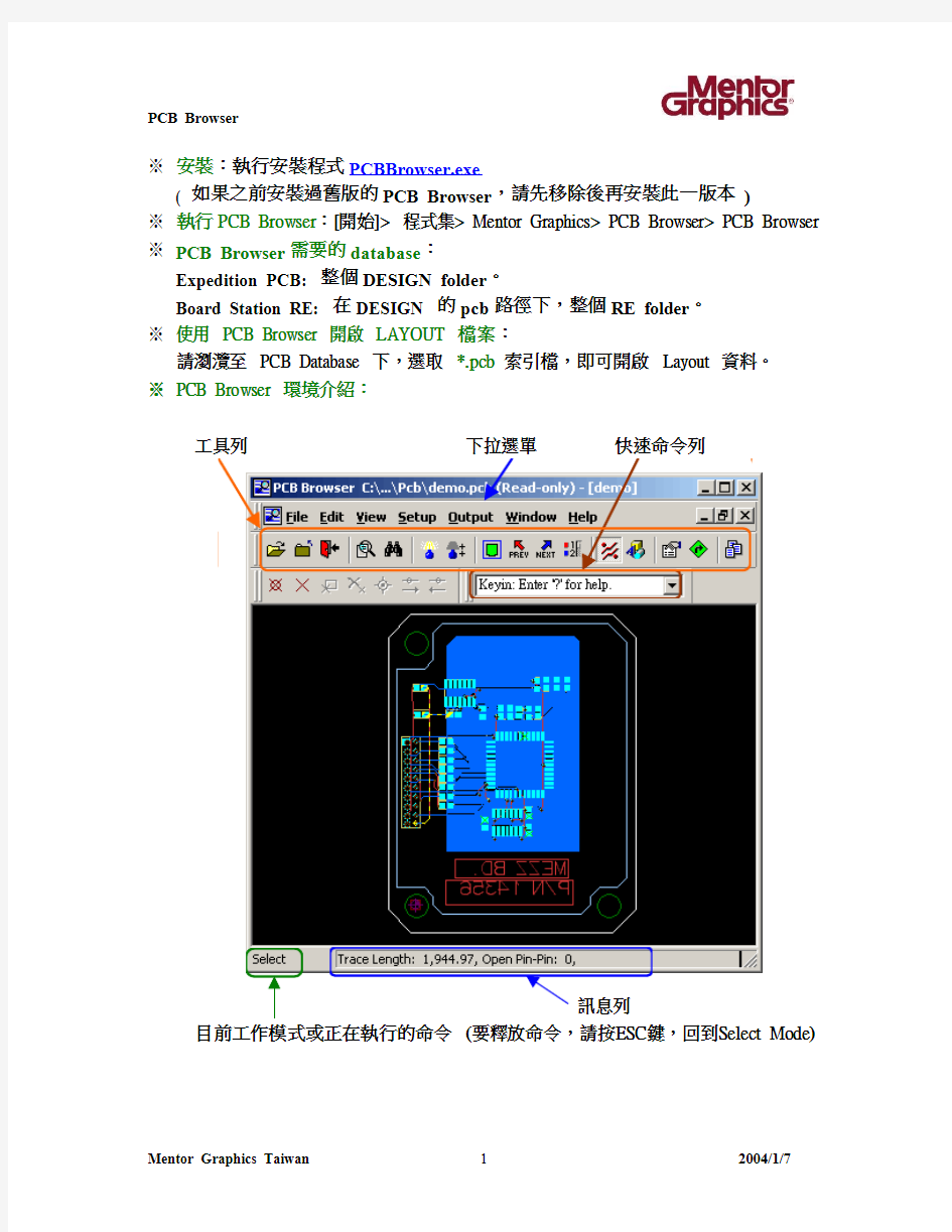
※ PCB Browser 環境介紹:
目前工作模式或正在執行的命令 (要釋放命令,請按ESC鍵,回到Select Mode)
※下拉選單:
File Menu Edit Menu
( 開啟PCB檔案) ( 複製選擇區域至剪貼簿 )
( 關閉目前PCB檔案)
( 設定printer參數)
( 列印預覽) (搜尋Part, Net, NetClass)
( 列印)
( Highlight Selected )
( UnHighlight Selected )
( UnHighlight All )
( 檢視選取的物件屬性) ( 離開PCB Browser )
Edit> Review Menu
( 檢視Board Information )
( 量測兩物件間距)
( 檢視選取的 Padstack 訊息)
View Menu標準工具列)
( 各物件顏色設定及開關
快速命令工具列)
自訂工具列)
( 設定Mouse中鍵為Stroke功能)
( Part DataBase, PCB Browser 無法使用)
( Board 參數定義,包括layers, layer stackup, vias rule & planes 定義)
( Router 環境設定,PCB Browser 無法修改)
( 檢視一般 Physical Rules,包括Net Type & Clearance Rules )
( 檢視High Speed Rules ,包括Max Length, Differential Pairs, Max Vias ) ( 數字表示法與精密度設定)
定義線寬、Routing Via
Via Type Routing Via
最小線寬線寬阻抗值最大線寬 Differential
Pair 間距
Setup> Net Classes and Clearances – Clearances
定義各物件的間距規則、群組與群組的間距規則
Setup> Net Property – Net Rules - Net Order
(Topology - 改變連接順序 )
Setup> Net Property – Net Rules – Net Order
( Net Group )
( Differential Pairs )
Setup> Net Property – Net Rules – Other
Define: Stub Length Max Vias
PIN A PIN B PIN C …
U2-36 to R105-2=1500 mils
Pin to Pin Length
Setup> Unit Display
:設定數字格式及數字精密度。
Output> Design Status…
:輸出該設計的所有與Board相關訊息至檔案,如下 。
==================================================== DESIGN STATUS
==================================================== Board Size Extents ............ 2.52 X 3.2 (in)
Route Border Extents .......... 2.52 X 3.2 (in)
Actual Board Area ............. 7.62 (in)
Actual Route Area ............. 7.62 (in)
Placement Areas: Name Available Required
Required/Available --- Entire Board 15.23 Sq. (in) 1.29 Sq. (in) 8.48 % Pins (140)
Pins per Route Area ........... 18.38 Pins/Sq. (in)
Layers (4)
Layer 1 is a signal layer : Trace Widths .......... 8, 25
Layer 2 is a Negative Plane Layer with nets +12V
Trace Widths .......... None.
Layer 3 is a Negative Plane Layer with nets GROUND
Trace Widths .......... None.
Layer 4 is a signal layer Trace Widths (8)
Nets (32)
Connections (61)
Open Connections (4)
Differential Pairs (2)
Differential Pair Names: /N$1297 /N$1298 /N$1299 /N$1300
Percent Routed ................ 93.44 %
Netline Length ................ 4.64 (in)
Netline Manhattan Length ...... 5.65 (in)
Total Trace Length ............ 25.44 (in)
Trace Widths Used (th) ........ 8, 25
Vias (15)
Via Span Name Quantity
1-4 via025_13 15 Teardrops 0
Breakouts 0
Virtual Pins 0
Guide Pins 0
Parts Placed (28)
Parts Mounted on Top (28)
SMD (22)
Through (6)
Test Points 0
Mechanical 0
Parts Mounted on Bottom 0
SMD 0
Through 0
Test Points 0
Mechanical 0
Edge Connector Parts 0
Parts not Placed 0
Nested Cells 0
Jumpers 0
Through Holes (30)
Holes per Board Area ...... 3.94 Holes/Sq. (in)
====================================================
※Dispay Control 層面及物件開關設定:
All Traces ON/OFF All Pads ON/OFF
各層面Pads開關
各層面Trace顏色設定 各層面Pads顏色設定 屬線顏色及開關 如有未完成的Trace線段
格點開關
陰影模式
設定Highlight顏色 (其他未被選中的線段,
以灰暗顏色表示 )
Board_Outline
Board_Outline
for Expedition
按著右鍵不放,上下左右
背景色
背面視角圖
關閉全部正面零件項目
項目
零件外型
PIN No.
Reference Designator
依Net Name來
定義顏色 來定義顏色
Planes (銅箔) 上
※Stroke Function 筆勢命令
Stroke 命令,是Mentor慣用來呼叫常用功能的簡便方式。你只要按住滑鼠中間(或右)鍵,畫出下列符號,即可呼叫出各項功能。
在PCB Browser環境中,你可以使用底下Stroke 命令:
Report Route-Mode Draw Mode
Zoom-In Zoom-Out View-Area View-All
Un-Select Display-Control Editor-Control
僅顯示編輯層的開關屬線開關
PCB Browser 常用功能介紹:
1. Trace 選擇規則:
(1) 選取一節線段(Trace Segment): 在該節線段上,按一下左鍵。
1 2 report info.
(2) 選取PIN to PIN 或PIN to T-Junction 線段: 在該節線段上,按二下左鍵。
(3) 選取整條線段: 在該節線段上,按三下左鍵。
(4) 選取一段區間線段: 在開始端按一下左鍵,按著右鍵移動視窗至末端,
並在末端再按一下左鍵,即可選取到該區間的線段。
1
2
2. Report 方法:
(1) 選取物件Trace,Via, Pin or Part,再按中間鍵畫出 Report Stroke 。
(2) 選取物件Trace,Via, Pin or Part,再按下工具列的 Report Function 。
(3) 選取物件Trace,Via, Pin or Part,查看訊息列。
3. 量測最短間距與Report Padstack information:
選取兩個物件( Trace,Via, Pin or Part ),可以同時按著Ctrl 鍵來重複選擇,再執行:File > Edit > Review> Minimum Distance : 量測兩物件(Trace, Via or Pin)的間距。
Padstack:報告padstack的尺寸、net name、所在座標及角度等訊息。
4. 尋找Net, Part or Net Type ( Net Class ):
(1) ”G、R”鍵,會自動找到第一條
(2) 尋找Component、Pin or Part_No.:
尋找 Component,請雙擊點選
尋找 Pin,請雙擊點選