High Speed Optocoupler, 100 kBd,
Low Input Current, Photodiode Darlington Output
https://www.doczj.com/doc/d98764585.html, For technical questions, contact: optocoupler.answers@https://www.doczj.com/doc/d98764585.html,
Document Number: 83605
6N138/6N139
Vishay Semiconductors
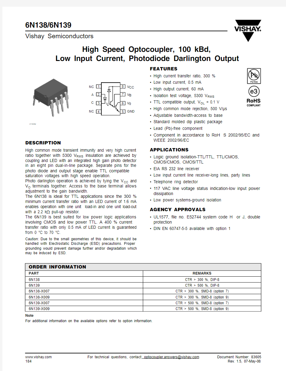
DESCRIPTION
High common mode transient immunity and very high current ratio together with 5300 V RMS insulation are achieved by coupling and LED with an integrated high gain photo detector in an eight pin dual-in-line package. Separate pins for the photo diode and output stage enable TTL compatible saturation voltages with high speed operation.
Photo darlington operation is achieved by tying the V CC and V O terminals together. Access to the base terminal allows adjustment to the gain bandwidth.
The 6N138 is ideal for TTL applications since the 300 %minimum current transfer ratio with an LED current of 1.6 mA enables operation with one unit load-in and one unit load-out with a 2.2 k Ω pull-up resistor.
The 6N139 is best suited for low power logic applications involving CMOS and low power TTL. A 400 % current transfer ratio with only 0.5 mA of LED current is guaranteed from 0 °C to 70 °C.
Caution: Due to the small geometries of this device, it should be handled with Electrostatic Discharge (ESD) precautions. Proper grounding would prevent damage further and/or degradation which may be induced by ESD.
FEATURES
?High current transfer ratio, 300 %
?Low input current, 0.5 mA
?High output current, 60 mA ?Isolation test voltage, 5300 V RMS ?TTL compatible output, V OL = 0.1 V ?High common mode rejection, 500 V/μs ?Adjustable bandwidth-access to base ?Standard molded dip plastic package ?Lead (Pb)-free component
?Component in accordance to RoH S 2002/95/EC and WEEE 2002/96/EC
APPLICATIONS
?Logic ground isolation-TTL/TTL, TTL/CMOS,CMOS/CMOS, CMOS/TTL ?EIA RS 232 line receiver
?Low input current line receiver-long lines, party lines ?Telephone ring detector
?117 VAC line voltage status indication-low input power dissipation
?Low power systems-ground isolation
AGENCY APPROVALS
?UL1577, file no. E52744 system code H or J, double protection
?DIN EN 60747-5-5 available with option 1
Note
For additional information on the available options refer to option information.
ORDER INFORMATION
PART REMARKS 6N138CTR > 300 %, DIP-86N139CTR > 500 %, DIP-86N138-X007CTR > 300 %, SMD-8 (option 7)6N138-X009CTR > 300 %, SMD-8 (option 9)6N139-X007CTR > 500 %, SMD-8 (option 7)6N139-X009
CTR > 500 %, SMD-8 (option 9)
Document Number: 83605For technical questions, contact: optocoupler.answers@https://www.doczj.com/doc/d98764585.html,
https://www.doczj.com/doc/d98764585.html,
6N138/6N139
High Speed Optocoupler, 100 kBd, Low Input Current, Photodiode Darlington
Output
Vishay Semiconductors Notes (1)T amb = 25 °C, unless otherwise specified. Stresses in excess of the absolute maximum ratings can cause permanent damage to the device.Functional operation of the device is not implied at these or any other conditions in excess of those given in the operational sections of this document. Exposure to absolute maximum ratings for extended periods of the time can adversely affect reliability.(2)Derate linearly above 50 °C free-air temperature at a rate of 0.4 mA/°C.(3)Derate linearly above 50 °C free-air temperature at a rate of 0.7 mW/°C.(4)Derate linearly above 25 °C free-air temperature at a rate of 0.7 mA/°C.(5)Derate linearly above 25 °C free-air temperature at a rate of 2.0 mW/°C.
(6)Refer to reflow profile for soldering conditions for surface mounted devices (SMD). Refer to wave profile for soldering conditions for through hole devices (DIP).
ABSOLUTE MAXIMUM RATINGS (1)
PARAMETER TEST CONDITION
PART
SYMBOL
VALUE
UNIT
INPUT
Reverse voltage V R 5.0V Forward current I F 25mA Average input current I f(avg)20mA Input power dissipation (2)(4)P diss
35
mW
OUTPUT
Supply and output voltage Pin 8 to 5, pin 6 to 56N138V CC , V O - 0.5 to 7.0V Pin 8 to 5, pin 6 to 5
6N139
V CC , V O
- 0.5 to 18
V Emitter base reverse voltage pin 5 to 7
0.5V Peak input current
50 % duty cycle - 1.0 ms
pulse width 40mA Peak transient input current t p ≤ 1.0 μs, 300 pps
1.0A Output current
Pin 6
I O 60mA Output power dissipation (3)(5)P diss
100
mW
COUPLER
Isolation test voltage V ISO 5300V RMS Isolation resistance V IO = 500 V, T amb = 25 ° C R IO ≥ 1012ΩV IO = 500 V, T amb = 100 ° C
R IO ≥ 1011ΩStorage temperature T stg - 55 to + 125°C Operating temperature T amb - 55 to + 100
°C Lead soldering temperature (6)
t = 10 s
T sld
260
°C
ELECTRICAL CHARACTERISTICS (1)
PARAMETER TEST CONDITION
PART
SYMBOL
MIN.
TYP.
MAX.
UNIT
INPUT
Input forward voltage
I F = 1.6 mA V F 1.4
1.7
V Input reverse breakdown voltage I R = 10 μA B VR
5.0
V Temperature coefficient of forward voltage
I F = 1.6 mA
- 1.8mV/°C
https://www.doczj.com/doc/d98764585.html, For technical questions, contact: optocoupler.answers@https://www.doczj.com/doc/d98764585.html,
Document Number: 83605
6N138/6N139
Vishay Semiconductors
High Speed Optocoupler, 100 kBd, Low Input Current, Photodiode Darlington
Output
Notes (1)T amb = 25 °C, unless otherwise specified. Minimum and maximum values are testing requirements. Typical values are characteristics of the device and are the result of engineering evaluation. Typical values are for information only and are not part of the testing requirements.(2)Pin 7 open.
(3)Device considered a two-terminal device: pins 1, 2, 3 and 4 shorted together and pins 5, 6, 7, and 8 shorted together.
Notes
(1)DC current transfer ratio is defined as the ratio of output collector current, I O , to the forward LED input current, I F times 100 %.(2)Pin 7 open.
Notes
(1)Pin 7 open.
(2)Using a resistor between pin 5 and 7 will decrease gain and delay time.
OUTPUT
Logic low, output voltage (2)
I F = 1.6 mA, I O = 4.8 mA,
V CC = 4.5 V
6N138V OL 0.10.4V I F = 1.6 mA, I O = 8.0 mA,
V CC = 4.5 V 6N139V OL 0.10.4V I F = 5.0 mA, I O = 15 mA,
V CC = 4.5 V 6N139V OL 0.150.4V I F = 12 mA, I O = 24 mA,
V CC = 4.5 V
6N139V OL 0.250.4V Logic high, output current (2)I F = 0 mA, V CC = 7.0 V 6N138I OH 0.1250μA I F = 0 mA, V CC = 18 V 6N139
I OH 0.05100μA Logic low supply current (2)I F = 1.6 mA, V O = OPEN,
V CC = 18 V I CCL 0.2 1.5mA Logic high supply current (2)I F = 0 mA, V O = OPEN,
V CC = 18 V
I CCH
0.001
10
μA
COUPLER Input capacitance
f = 1.0 MHz, V F = 0C IN
25
pF Input output insulation leakage current (3)
45 % relative humidity, T amb = 25 °C, t = 5.0 s,
V IO = 3000 VDC
1.0
μA Resistance (input to output) (3)V IO = 500 VDC R IO 1012ΩCapacitance (input to output) (3)
f = 1.0 MHz
C IO
0.6
pF
CURRENT TRANSFER RATIO
PARAMETER
TEST CONDITION PART SYMBOL MIN.TYP.MAX.
UNIT Current transfer ratio (1)(2)
I F = 1.6 mA, V O = 0.4 V,
V CC = 4.5 V 6N138CTR 3001600%Current transfer ratio
I F = 0.5 mA, V O = 0.4 V,
V CC = 4.5 V 6N139CTR 4001600%I F = 1.6 mA, V O = 0.4 V,
V CC = 4.5 V
6N139
CTR
500
2000
%
SWITCHING CHARACTERISTICS
PARAMETER
TEST CONDITION PART SYMBOL MIN.
TYP.MAX.UNIT Propagation delay time to logic low at output
I F = 1.6 mA, R L = 2.2 k Ω6N138t PHL 2.010μs Propagation delay time to logic low at output (1)(2)
I F = 0.5 mA, R L = 4.7 k Ω6N139t PHL 6.025μs I F = 12 mA, R L = 270 Ω6N139t PHL
0.6
1.0μs Propagation delay time to logic high at output
I F = 1.6 mA, R L = 2.2 k Ω6N138t PLH 2.035μs I F = 0.5 mA, R L = 4.7 k Ω6N139t PLH 4.060μs Propagation delay time to logic high at output (1)(2)
I F = 12 mA, R L = 270 Ω
6N139
t PLH 1.5
7.0
μs
ELECTRICAL CHARACTERISTICS (1)
PARAMETER TEST CONDITION PART
SYMBOL
MIN.
TYP.
MAX.
UNIT
Document Number: 83605For technical questions, contact: optocoupler.answers@https://www.doczj.com/doc/d98764585.html,
https://www.doczj.com/doc/d98764585.html,
6N138/6N139
High Speed Optocoupler, 100 kBd, Low Input Current, Photodiode Darlington
Output
Vishay Semiconductors Notes
(1)Common mode transient immunity in logic high level is the maxium tolerable (positive) dVcm/dt on the leading edge of the common mode pulse, V CM , to assure that the output will remain in a logic high state (i.e. V O > 2.0 V) common mode transient immunity in logic low level is the maximum tolerable (negative) dVcm/dt on the trailing edge of the common mode pulse signal, V CM to assure that the output will remain in a logic low state (i.e. V O < 0.8 V).
(2)In applications where dV/dt may exceed 50 000 V/μs (such as state discharge) a series resistor, R CC should be included to protect I C
from destructively high surge currents. The recommend value is R CC ? [(1 V)/(0.15 I F (mA)] k Ω
PACKAGE DIMENSIONS in inches (millimeters)
COMMON MODE TRANSIENT IMMUNITY
PARAMETER
TEST CONDITION PART
SYMBOL MIN.
TYP.MAX.
UNIT Common mode transient immunity, logic high level output (1)(2)
I F = 0 mA, R L = 2.2 k Ω, R CC = 0, |V CM | = 10 V P-P |CM H |
500
V/μs
Common mode transient immunity, logic low level output (1)(2)
I F = 0 mA, R L = 2.2 k Ω,R CC = 0, |V CM | = 10 V P-P
|CM L |
-
500V/μs
6N138/6N139
Vishay Semiconductors High Speed Optocoupler, 100 kBd,
Low Input Current, Photodiode Darlington
Output
OZONE DEPLETING SUBSTANCES POLICY STATEMENT
It is the policy of Vishay Semiconductor GmbH to
1.Meet all present and future national and international statutory requirements.
2.Regularly and continuously improve the performance of our products, processes, distribution and operating systems with
respect to their impact on the health and safety of our employees and the public, as well as their impact on the environment. It is particular concern to control or eliminate releases of those substances into the atmosphere which are known as ozone depleting substances (ODSs).
The Montreal Protocol (1987) and its London Amendments (1990) intend to severely restrict the use of ODSs and forbid their use within the next ten years. Various national and international initiatives are pressing for an earlier ban on these substances. Vishay Semiconductor GmbH has been able to use its policy of continuous improvements to eliminate the use of ODSs listed in the following documents.
1.Annex A, B and list of transitional substances of the Montreal Protocol and the London Amendments respectively.
2.Class I and II ozone depleting substances in the Clean Air Act Amendments of 1990 by the Environmental Protection Agency
(EPA) in the USA.
3.Council Decision 88/540/EEC and 91/690/EEC Annex A, B and C (transitional substances) respectively.
Vishay Semiconductor GmbH can certify that our semiconductors are not manufactured with ozone depleting substances and do not contain such substances.
We reserve the right to make changes to improve technical design
and may do so without further notice.
Parameters can vary in different applications. All operating parameters must be validated for each customer application by the customer. Should the buyer use Vishay Semiconductors products for any unintended or unauthorized application, the buyer shall indemnify Vishay Semiconductors against all claims, costs, damages, and expenses, arising out of, directly or indirectly, any claim of personal damage, injury or death associated with such unintended or unauthorized use.
Vishay Semiconductor GmbH, P.O.B. 3535, D-74025 Heilbronn, Germany
https://www.doczj.com/doc/d98764585.html, For technical questions, contact: optocoupler.answers@https://www.doczj.com/doc/d98764585.html, Document Number: 83605
Disclaimer Legal Disclaimer Notice
Vishay
All product specifications and data are subject to change without notice.
Vishay Intertechnology, Inc., its affiliates, agents, and employees, and all persons acting on its or their behalf (collectively, “Vishay”), disclaim any and all liability for any errors, inaccuracies or incompleteness contained herein or in any other disclosure relating to any product.
Vishay disclaims any and all liability arising out of the use or application of any product described herein or of any information provided herein to the maximum extent permitted by law. The product specifications do not expand or otherwise modify Vishay’s terms and conditions of purchase, including but not limited to the warranty expressed therein, which apply to these products.
No license, express or implied, by estoppel or otherwise, to any intellectual property rights is granted by this document or by any conduct of Vishay.
The products shown herein are not designed for use in medical, life-saving, or life-sustaining applications unless otherwise expressly indicated. Customers using or selling Vishay products not expressly indicated for use in such applications do so entirely at their own risk and agree to fully indemnify Vishay for any damages arising or resulting from such use or sale. Please contact authorized Vishay personnel to obtain written terms and conditions regarding products designed for such applications.
Product names and markings noted herein may be trademarks of their respective owners.
Document Number: https://www.doczj.com/doc/d98764585.html,