74AC240, 74ACT240 — Octal Buffer/Line Driver with 3-STATE Outputs
Octal Buffer/Line Driver with 3-STATE Outputs
Features
■I CC and I OZ reduced by 50%
■Inverting 3-STATE outputs drive bus lines or buffer
memory address registers ■Outputs source/sink 24mA
■ACT240 has TTL-compatible inputs
General Description
The AC/ACT240 is an octal buffer and line driver designed to be employed as a memory address driver,clock driver and bus oriented transmitter or receiver which provides improved PC board density.
Ordering Information
Device also available in Tape and Reel. Specify by appending suffix letter “X” to the ordering number.
All packages are lead free per JEDEC: J-STD-020B standard.
Order Number
Package Number
Package Description
74AC240SC M20B 20-Lead Small Outline Integrated Circuit (SOIC), JEDEC MS-013, 0.300" Wide 74AC240SJ M20D 20-Lead Small Outline Package (SOP), EIAJ TYPE II, 5.3mm Wide
74AC240MTC MTC2020-Lead Thin Shrink Small Outline Package (TSSOP), JEDEC MO-153, 4.4mm Wide
74AC240PC N20A 20-Lead Plastic Dual-In-Line Package (PDIP), JEDEC MS-001, 0.300" Wide 74ACT240SC M20B 20-Lead Small Outline Integrated Circuit (SOIC), JEDEC MS-013, 0.300" Wide 74ACT240SJ M20D 20-Lead Small Outline Package (SOP), EIAJ TYPE II, 5.3mm Wide
74ACT240MTC MTC2020-Lead Thin Shrink Small Outline Package (TSSOP), JEDEC MO-153, 4.4mm Wide
74ACT240PC
N20A
20-Lead Plastic Dual-In-Line Package (PDIP), JEDEC MS-001, 0.300" Wide
74AC240, 74ACT240 — Octal Buffer/Line Driver with 3-STATE Outputs
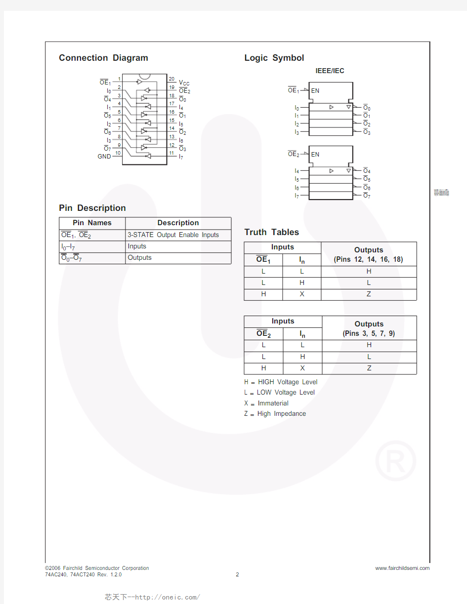
Pin Description
Truth Tables
H = HIGH Voltage Level L = LOW Voltage Level X = Immaterial Z = High Impedance
Pin Names
Description
OE 1, OE 23-STATE Output Enable Inputs
I 0–I 7Inputs O 0–O 7
Outputs
5678910
161514131211
O 5
I 2
O 6
I 3
O 7
GND
O 1I 5O 2I 6O 3I 7
Inputs Outputs
(Pins 12, 14, 16, 18)
OE 1
I n
L L H L H L H
X
Z
Inputs Outputs (Pins 3, 5, 7, 9)
OE 2
I n
L L H L H L H
X
Z
O 1I 1O 2I 2O 3
I 3
O 4I 4O 5I 5O 6I 6O 7
I 7
OE 2EN
74AC240, 74ACT240 — Octal Buffer/Line Driver with 3-STATE Outputs
Recommended Operating Conditions
The Recommended Operating Conditions table defines the conditions for actual device operation. Recommended operating conditions are specified to ensure optimal performance to the datasheet specifications. Fairchild does not recommend exceeding them or designing to absolute maximum ratings.
V CC Supply Voltage ?0.5V to +7.0V
I IK
DC Input Diode Current V I = ?0.5V ?20mA V I = V CC + 0.5
+20mA
V I DC Input Voltage ?0.5V to V CC + 0.5V
I OK
DC Output Diode Current V O = ?0.5V ?20mA V O = V CC + 0.5V
+20mA
V O DC Output Voltage
?0.5V to V CC + 0.5V
I O DC Output Source or Sink Current ±50mA I CC or I GND DC V CC or Ground Current per Output Pin
±50mA
T STG Storage Temperature ?65°C to +150°C
T J
Junction Temperature
140°C
Symbol Parameter
Rating
V CC
Supply Voltage AC 2.0V to 6.0V ACT
4.5V to
5.5V V I Input Voltage 0V to V CC V O Output Voltage 0V to V CC
T A Operating Temperature
?40°C to +85°C
?V / ?t Minimum Input Edge Rate, AC Devices:
V IN from 30% to 70% of V CC , V CC @ 3.3V , 4.5V , 5.5V 125mV/ns ?V / ?t
Minimum Input Edge Rate, ACT Devices: V IN from 0.8V to 2.0V , V CC @ 4.5V , 5.5V
125mV/ns
Notes:
1.All outputs loaded; thresholds on input associated with output under test.
2.I IN and I CC @
3.0V are guaranteed to be less than or equal to the respective limit @ 5.5V V CC .3.Maximum test duration 2.0ms, one output loaded at a time.
5.5
V IN = V IL or V IH ,I OL = 24mA (1)0.360.44I IN (2)Maximum Input Leakage Current 5.5V I = V CC , GND ±0.1±1.0μA I OZ
Maximum 3-STATE Leakage Current 5.5
V I (OE) = V IL , V IH ; V I = V CC , GND; V O = V CC , GND ±0.25
±2.5
μA I OLD Minimum Dynamic Output Current (3) 5.5V OLD = 1.65V Max.75mA I OHD 5.5V OHD = 3.85V Min.-75
mA I CC (2)
Maximum Quiescent Supply Current
5.5
V IN = V CC or GND
4.0
40.0
μA
Notes:
4.All outputs loaded; thresholds on input associated with output under test.
5.Maximum test duration 2.0ms, one output loaded at a time.
OHD OHD I CC
Maximum Quiescent Supply Current
5.5
V IN = V CC or GND
4.040.0
μA
Note:
7.Voltage range 5.0 is 5.0V ± 0.5V.
Capacitance
t PHL Propagation Delay, Data to Output 5.0 1.5 5.57.5 1.58.5ns t PZH Output Enable Time 5.0 1.57.08.5 1.09.5ns t PZL Output Enable Time 5.0 2.07.09.5 1.510.5ns t PHZ Output Disable Time 5.0 2.08.09.5 2.010.5ns t PLZ
Output Disable Time
5.0
2.5
6.5
10.0
2.0
10.5
ns
Symbol
Parameter
Conditions
Typ.
Units
C IN Input Capacitance
V CC = OPEN 4.5pF C PD
Power Dissipation Capacitance
V CC = 5.0V
45.0
pF
Figure 1. 20-Lead Small Outline Integrated Circuit (SOIC), JEDEC MS-013, 0.300" Wide
Package drawings are provided as a service to customers considering Fairchild components. Drawings may change in any manner without notice. Please note the revision and/or date on the drawing and contact a Fairchild Semiconductor representative to verify or obtain the most recent revision. Package speci?cations do not expand the terms of Fairchild’s worldwide terms and conditions, speci?cally the warranty therein, which covers Fairchild products.
Always visit Fairchild Semiconductor’s online packaging area for the most recent package drawings:https://www.doczj.com/doc/d08484962.html,/packaging/
MS-013,VARIATION AC,ISSUE E
B)ALL DIMENSIONS ARE IN MILLIMETERS.C)DIMENSIONS DO NOT INCLUDE MOLD
FLASH OR BURRS.
E)LANDPATTERN STANDARD:SOIC127P1030X265-20L 8°0°
SEATING PLANE
DETAIL A
SCALE:2:1
F)DRAWING FILENAME:MKT-M20BREV3
(R0.10)
1.270.40(1.40)
0.25
D)CONFORMS TO ASME Y14.5M-1994
Figure 2. 20-Lead Small Outline Package (SOP), EIAJ TYPE II, 5.3mm Wide
Package drawings are provided as a service to customers considering Fairchild components. Drawings may change in any manner without notice. Please note the revision and/or date on the drawing and contact a Fairchild Semiconductor representative to verify or obtain the most recent revision. Package speci?cations do not expand the terms of Fairchild’s worldwide terms and conditions,
Figure 3. 20-Lead Thin Shrink Small Outline Package (TSSOP), JEDEC MO-153, 4.4mm Wide
Package drawings are provided as a service to customers considering Fairchild components. Drawings may change in any manner without notice. Please note the revision and/or date on the drawing and contact a Fairchild Semiconductor representative to verify or obtain the most recent revision. Package speci?cations do not expand the terms of Fairchild’s worldwide terms and conditions,
NOTES:
Figure 4. 20-Lead Plastic Dual-In-Line Package (PDIP), JEDEC MS-001, 0.300" Wide
Package drawings are provided as a service to customers considering Fairchild components. Drawings may change in any manner without notice. Please note the revision and/or date on the drawing and contact a Fairchild Semiconductor representative to verify or obtain the most recent revision. Package speci?cations do not expand the terms of Fairchild’s worldwide terms and conditions, speci?cally the warranty therein, which covers Fairchild products.
Always visit Fairchild Semiconductor’s online packaging area for the most recent package drawings:
subsidiaries,and is not intended to be an exhaustive list of all such trademarks.
ACEx ?
Build it Now ?CorePLUS ?CROSSVOLT ?CTL?
Current Transfer Logic?EcoSPARK ?EZSWITCH?*
?
?
Fairchild
?Fairchild Semiconductor ?FACT Quiet Series?FACT ?FAST ?FastvCore ?FlashWriter ?*
FPS ?FRFET ?
Global Power Resource SM Green FPS ?
Green FPS ?e-Series ?GTO ?i-Lo ?
IntelliMAX ?ISOPLANAR ?MegaBuck?
MICROCOUPLER ?MicroFET ?MicroPak ?MillerDrive?Motion-SPM?OPTOLOGIC ?OPTOPLANAR ?
?
PDP-SPM?Power220?
Power247?
POWEREDGE ?Power-SPM ?PowerTrench ?
Programmable Active Droop ?QFET ?
QS ?QT Optoelectronics ?Quiet Series ?RapidConfigure ?SMART START ?SPM ?STEALTH?SuperFET ?SuperSOT ?-3SuperSOT ?-6SuperSOT ?-8
SyncFET?
?
The Power Franchise ?TinyBoost ?
TinyBuck ?TinyLogic ?
TINYOPTO ?TinyPower ?TinyPWM ?
TinyWire ?μSerDes ?
UHC ?
Ultra FRFET ?
UniFET ?VCX ?*EZSWITCH?and FlashWriter ?
are trademarks of System General Corporation,used under license by Fairchild Semiconductor.
DISCLAIMER
FAIRCHILD SEMICONDUCTOR RESERVES THE RIGHT TO MAKE CHANGES WITHOUT FURTHER NOTICE TO ANY PRODUCTS HEREIN TO IMPROVE RELIABILITY,FUNCTION,OR DESIGN.FAIRCHILD DOES NOT ASSUME ANY LIABILITY ARISING OUT OF THE APPLICATION OR USE OF ANY PRODUCT OR CIRCUIT DESCRIBED HEREIN;NEITHER DOES IT CONVEY ANY LICENSE UNDER ITS PATENT RIGHTS,NOR THE RIGHTS OF OTHERS.THESE SPECIFICATIONS DO NOT EXPAND THE TERMS OF FAIRCHILD’S WORLDWIDE TERMS AND CONDITIONS,SPECIFICALLY THE WARRANTY THEREIN,WHICH COVERS THESE PRODUCTS.LIFE SUPPORT POLICY
FAIRCHILD’S PRODUCTS ARE NOT AUTHORIZED FOR USE AS CRITICAL COMPONENTS IN LIFE SUPPORT DEVICES OR SYSTEMS WITHOUT THE EXPRESS WRITTEN APPROVAL OF FAIRCHILD SEMICONDUCTOR CORPORATION.As used herein:
1.Life support devices or systems are devices or systems which,(a)are intended for surgical implant into the body or (b)support or sustain life,and (c)whose failure to perform when properly used in accordance with instructions for use provided in the labeling,can be reasonably expected to result in a significant injury of the user.
2.A critical component in any component of a life support,device,or system whose failure to perform can be reasonably expected to cause the failure of the life support device or system,or to affect its safety or effectiveness.
PRODUCT STATUS DEFINITIONS Definition of Terms Datasheet Identification Product Status Definition
Advance Information
Form First Production
ative or In Design
This datasheet contains the design specifications for product
development.Specifications may change in any manner without notice.Preliminary
This datasheet contains preliminary data;supplementary data will be published at a later date.Fairchild Semiconductor reserves the right to make changes at any time without notice to improve design.
74AC240, 74ACT240 — Octal Buffer/Line Driver with 3-STATE Outputs