MODIFYING USER-DEFINED LOGIC FOR TEST ACCESS
TO EMBEDDED CORES
Bahram Pouya and Nur A. Touba
Computer Engineering Research Center
Department of Electrical and Computer Engineering
University of Texas, Austin, TX 78712-1084
Abstract
Testing embedded cores is a challenge because access to core I/Os is limited. The user-defined logic (UDL) surrounding the core may restrict the set of test vectors that can be applied to the core. This is especially a problem for intellectual property cores and legacy design cores where the set of test vectors used to test the core is “fixed” independent of the design in which the core is embedded (i.e., the vectors are not selected using an ATPG procedure that considers the overall circuit, core plus UDL). Consequently, some of the specified core test vectors may not be contained in the output space of the UDL that drives the core and hence cannot be justified at the core inputs. Conventional solutions to this problem involve placing multiplexers or boundary scan elements at the inputs of the core to provide test access. This can be very costly in terms of area and performance. This paper presents a procedure for inserting control points in the UDL to modify its output space so that it contains the specified core test vectors. The flexibility in selecting the location of the control points is used to avoid performance degradation by keeping test logic off the critical timing paths. Experimental results are shown comparing the control point insertion procedure with other approaches.
1. Introduction
In order to shorten product development cycles for integrated circuits and systems, a growing trend is to make use of pre-designed blocks, called cores. Testing cores embedded within a larger design can be a significant challenge because there is limited access to the core I/Os. The set of vectors that can be justified at the inputs of a core is restricted to those that exist in the output space of the user-defined logic (UDL) driving the core. There are two important cases where the particular set of test vectors that are to be used to test a core are “fixed” independent of the design in which the core is embedded (i.e., the vectors are not selected using an ATPG procedure that considers the overall circuit, core plus UDL). The first case is where the core supplier considers the core to be intellectual property and thus is not willing to give any information about the internal logic of the core (i.e., it is a black box). In that case, the traditional test generation process such as ATPG and fault simulation cannot be performed. The core vendor specifies the set of test vectors that must be applied to the core to guarantee a sufficient fault coverage. The second case where the core test vectors may be “fixed” is if the core is a legacy design (i.e., an existing design that is being re-used) for which it is desirable to use existing test vectors rather than expending new effort in test generation. In both of these cases, some of the core test vectors may not be contained in the output space of the UDL driving the core, and hence some design-for-testability (DFT) is required in order to apply the vectors to the core.
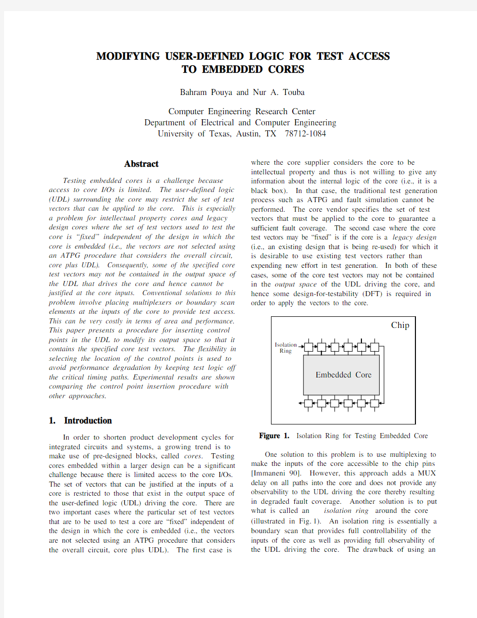
Figure 1. Isolation Ring for Testing Embedded Core
One solution to this problem is to use multiplexing to make the inputs of the core accessible to the chip pins [Immaneni 90]. However, this approach adds a MUX delay on all paths into the core and does not provide any observability to the UDL driving the core thereby resulting in degraded fault coverage. Another solution is to put what is called an isolation ring around the core (illustrated in Fig.1). An isolation ring is essentially a boundary scan that provides full controllability of the inputs of the core as well as providing full observability of the UDL driving the core. The drawback of using an
isolation ring is the large area and performance overhead that it adds. A boundary scan element and associated routing is required for each input of the core, and a MUX delay is added to every path into the core (as illustrated in Fig. 2). As a result, using a full isolation ring is undesirable, especially in high performance applications.Recently a partial isolation ring approach was presented in [Touba 97]. It reduces the number of isolation ring elements while still providing the same fault coverage as a full isolation ring. This is accomplished by justifying part of each core test vector through the UDL.
Figure 2. Conventional Approach with Isolation Ring at
Inputs of Embedded Core Bhatia, et. al, at CrossCheck [Bhatia 96] introduced a grid-based direct access methodology for testing core-based designs. This method differs from the embedded grid test method described in [Gheewala 89]and [Chandra 91], in that it uses a “soft” netlist level grid as opposed to a “hard” grid embedded at the base of gate arrays. The “soft” netlist level grid described in [Bhatia 96] provides direct access to storage elements,observation test points, and bi-directional test points via the chip pins. The basic approach is to place
bi-directional test points at the inputs and outputs of the embedded core, and matrix accessible storage elements and observation test points in the user-defined logic to provide sufficient fault coverage. This approach requires new library cells to implement the matrix accessible storage elements, bi-directional test points, and I/O pads,and it requires global routing of the test grid.
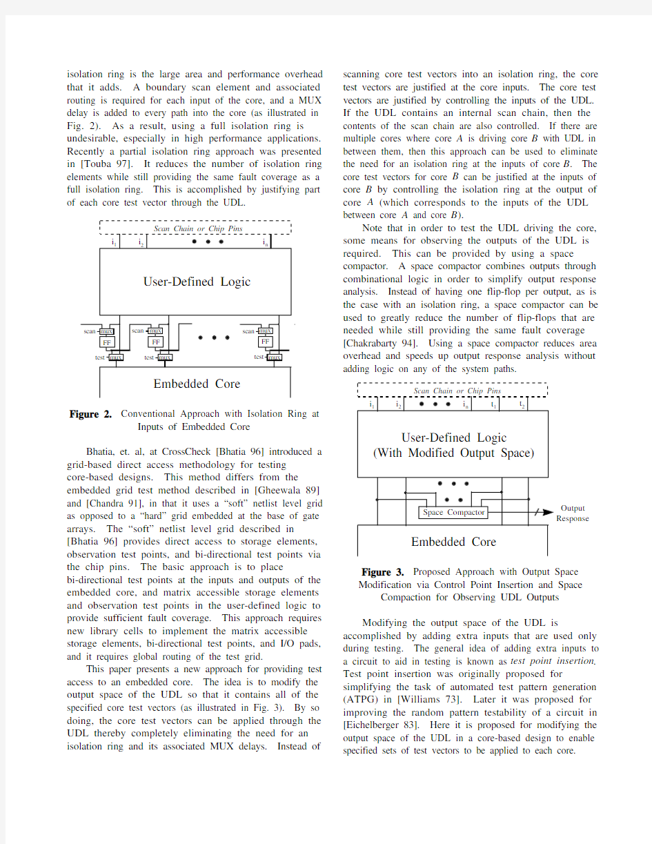
This paper presents a new approach for providing test access to an embedded core. The idea is to modify the output space of the UDL so that it contains all of the specified core test vectors (as illustrated in Fig. 3). By so doing, the core test vectors can be applied through the UDL thereby completely eliminating the need for an isolation ring and its associated MUX delays. Instead of
scanning core test vectors into an isolation ring, the core test vectors are justified at the core inputs. The core test vectors are justified by controlling the inputs of the UDL.If the UDL contains an internal scan chain, then the contents of the scan chain are also controlled. If there are multiple cores where core A is driving core B with UDL in between them, then this approach can be used to eliminate the need for an isolation ring at the inputs of core B . The core test vectors for core B can be justified at the inputs of core B by controlling the isolation ring at the output of core A (which corresponds to the inputs of the UDL between core A and core B ).
Note that in order to test the UDL driving the core,some means for observing the outputs of the UDL is required. This can be provided by using a space compactor. A space compactor combines outputs through combinational logic in order to simplify output response analysis. Instead of having one flip-flop per output, as is the case with an isolation ring, a space compactor can be used to greatly reduce the number of flip-flops that are needed while still providing the same fault coverage [Chakrabarty 94]. Using a space compactor reduces area overhead and speeds up output response analysis without adding logic on any of the system paths.
Output Response
Figure 3. Proposed Approach with Output Space Modification via Control Point Insertion and Space
Compaction for Observing UDL Outputs
Modifying the output space of the UDL is accomplished by adding extra inputs that are used only during testing. The general idea of adding extra inputs to a circuit to aid in testing is known as test point insertion .Test point insertion was originally proposed for simplifying the task of automated test pattern generation (ATPG) in [Williams 73]. Later it was proposed for improving the random pattern testability of a circuit in [Eichelberger 83]. Here it is proposed for modifying the output space of the UDL in a core-based design to enable specified sets of test vectors to be applied to each core.
X X X X X t 1t 2X X X X X Control Point 9 Patterns in Ouput Space
16 Patterns in Ouput Space
Figure 4. Example of Modifying Output Space by Inserting Control Points
Whereas using an isolation ring or using MUXed inputs to apply test vectors to the core adds a MUX delay to every path, inserting control points in the UDL only adds delay to some of the paths. By carefully selecting the location of the control points, the critical timing paths can be avoided so that system performance is not degraded.Putting multiplexers on every output of the UDL is a simple brute force way to modify the output space, but it is very costly in terms of area and performance. The technique described here is a more efficient and low-cost way to modify the output space of the UDL to provide test access to an embedded core.
The paper is organized as follows: In Sec. 2, the use of control points for modifying the output space of the UDL is described. In Sec. 3, the concepts and strategies that form the basis for the proposed control point insertion procedure are explained. In Sec. 4, a step by step description of the control point insertion procedure is given. Each step is illustrated on an example circuit. In Section 5, experimental results are shown for the control point insertion procedure and the overhead is compared with that for using full and partial isolation rings. Section 6 is a summary and conclusion.
2. Modifying Output Space
The technique described in this paper involves modifying the output space of the UDL while still allowing it to perform its intended function during system mode. The means for accomplishing this is to insert control points in the UDL which can be used during test mode to control the value at certain nodes in order to justify particular output vectors. In the example in Fig. 4,the output space of the circuit contains only 9 of the 16possible patterns. A control point is inserted to fix the logic value at the input of gates G1 and G2 to a 1 when the control point is activated (this is called a control-1
point ), and a control point is also added to fix the logic value at the input of gate G4 to a 0 when the control point is activated (this is called a control-0 point ). These two control points allow all 16 possible patterns to be justified during test mode. During system mode, the t 1 and t 2inputs are set to 0, so the control points are not activated and thus don't affect the system function. However,control points do add an extra level of logic to some paths in the circuit. If a control point is placed on a critical timing path, it can increase the delay through the circuit,so care must be taken in selecting the location of the control points.
3. Strategy For Inserting Control Points
This section describes several important concepts and strategies that form the basis for the proposed control point insertion procedure for modifying the output space of the UDL. Given a specified core test vector that cannot be justified through the UDL, there are two basic steps:the first is to identify conflicts that arise when trying to justify the vector, and the second is to insert control points to remove those conflicts so that the vector can be justified.
3.1 Identifying Conflicts
For each core test vector that is to be justified through the UDL, the values of the primary outputs are set to the corresponding values and backtracing towards the primary inputs is performed. If a fanout stem is reached where the values that are assigned on its branches are not all the same, a conflict occurs. If backtracing can be completed all the way to the primary inputs with no conflicts, then the output vector can be justified through the UDL using the input vector corresponding to the final values assigned to the primary inputs. Notice that if there is no fanout in
the circuit, no conflicts can occur. Hence, the output space of a fanout-free circuit contains all possible output vectors.
In backtracing through the circuit, two types of gates are encountered: “decision gates” and “imply gates.” If the value assigned to the output of a multi-input gate can be justified by assigning a value to only one of the inputs (e.g., justifying a 0 at the output of an AND gate), then the gate is said to be a decision gate since there is more than one way to backtrace through the gate. If justifying the value assigned to the output of a gate requires assigning values to all of the inputs (e.g., justifying a 1 at the output of an AND gate), then the gate is said to be an imply gate. In the example in Fig. 5, for output vector 0110, gates G1, G2, G3, and G5 are imply gates, while gate G6 is a decision gate.
X X
X X
X
1 2 Z 3
Z 4
Figure 5. Example of Backward Implications from
Primary Outputs
If a conflict occurs during backtracing, then it may be possible to avoid the conflict by choosing to backtrace down a different path in some decision gate. If all possible paths for backtracing result in a conflict(s), then a control point must be inserted to remove the conflict(s) to permit the core test vector to be justified through the UDL.
3.2 Imply and Decision Conflicts
Each conflict that is encountered during backtracing can be classified as either an “imply conflict” or a “decision conflict.” An imply conflict is one that occurs due to backtracing through imply gates only (i.e., no backtracing is done through decision gates), whereas a decision conflict is one that occurs due to backtracing through one or more decision gates. A decision conflict can be avoided by backtracing down a different path in some decision gate, whereas an imply conflict cannot be avoided because there are no decision gates between the primary outputs and the fanout point where the conflict occurs. In Fig. 5, the conflict at primary input X1 is an imply conflict because inconsistent values are implied on the fanout branches through imply gates only. For the decision gate G6, if backtracing is done down the input towards gate G3, then a decision conflict occurs at the output of gate G3, however, if backtracing is done down the other input towards gate G4, then a decision conflict occurs at primary input X4.
All imply conflicts must be removed with control points in order to justify the output vector. Some decision conflicts may also need to be removed, but there is more than one option as to which decision conflict is removed for justifying a particular output vector. When inserting control points to justify a set of vectors, a good strategy is to first insert control points to remove all of the imply conflicts for all of the vectors (since they must be removed in any solution) before removing decision conflicts. Consider the case where vector v1 can be justified by either removing decision conflict c1 or decision conflict c2, but for vector v2, conflict c2 is an imply conflict. Any solution will require that conflict c2 be removed, so removing conflict c1 would be superfluous. It is better to defer the selection of which decision conflicts to remove until all imply conflicts have been removed.
3.3 Removing Imply Conflicts
A conflict involves a fanout point in which some of the fanout branches have a 0 implied on them and some have a 1 implied on them. A control point must be inserted in order to change the implied values on the fanout branches so that they are all consistent (either all 1’s and X’s, or all 0’s and X’s). A conflict at a fanout point can be removed with a single control point. The set of branches with a 1 (0) can be controlled by a single control-1 (control-0) point that is placed between the fanout stem and the set of branches. Then all of the branches in the original fanout point will either have a 0 (1) or an X implied on them resulting in a consistent set of values with a 0 (1) being implied on the stem.
- OR -
Figure 6. Removing a Conflict with Either a Control-1
Point or a Control-0 Point.
Note that for any conflict, there are two ways to remove the conflict with a single control point: either a control-1 point can be inserted to control all of the
branches with a 1, or a control-0 point can be inserted to control all of the branches with a 0 (as illustrated in Fig. 6). If one or more of the branches is on a critical timing path, then the decision on which way to remove the conflict can be made based on minimizing the performance impact by keeping the control point off the critical timing paths if possible (it will always be possible if only one branch is on a critical timing path, but it may not be possible if multiple branches are on the critical timing path and have opposite logic values implied on them). If none of the branches are on the critical timing path, then the decision on which way to remove the conflict can be based on which value is better to imply on the stem. If it is easier to control the stem to a 1 (0), then a control-0 (control-1) point should be inserted to remove the conflict. Many methods for determining heuristic controllability values exist [Rutman 72], [Breuer 78],[Goldstein 79], [Brglez 84], etc. These controllability values can be used to determine whether it is easier to control a particular node in the circuit to a 1 or to a 0.
If the control point needs to be inserted on only one of the branches (i.e., only one branch has a conflicting logic value from the rest of the branches), then rather than inserting the control point right after the fanout point where the conflict occurs, it is better to insert the control point further down the circuit towards the primary outputs. The reason for this is that the control point reduces the number of backward implications that are made in the circuit as illustrated in Fig. 7. The question then is how far towards the primary outputs should the control point be placed. If the fanout branch where the conflict occurs propagates to only one primary output,then the best location to place the control point is right at the primary output. If the fanout branch where the conflict occurs (call it FB conflict ) propagates to multiple primary outputs then that means there is another fanout point (call it FP no_conflict ) further down the circuit where the path branches out towards multiple primary outputs.In that case, the strategy is to place the control point right before FP no_conflict (as illustrated in Fig. 7), because otherwise multiple control points would be needed to change the value on each branch of FP no_conflict t in order to
change the value that is implied on the stem at FP no_conflict (which is necessary to remove the conflict at FB conflict ). So the idea is to use only one control point to remove the conflict at FB conflict , and to place that control point as far down the circuit towards the primary outputs as possible in order to remove as many backwards implications in the circuit as possible. The fewer backwards implications there are, the less chance there is for additional conflicts.
3.4 Removing Decision Conflicts
Once the imply conflicts have been removed for all of the core test vectors, then for the remaining vectors that still cannot be justified at the output of the UDL, some decision conflicts must be removed with control points.Unlike the case with imply conflicts, there is some flexibility in choosing which decision conflicts to remove.This flexibility can be used to avoid inserting control points on critical timing paths. The first criteria in selecting which decision conflicts to remove involves checking to see which can be removed without inserting logic on critical timing paths. As was described before, a conflict can be removed from a fanout point without adding logic on a critical timing path provided the fanout point does not have multiple branches that are on critical timing paths with opposite logic values implied on them.The decision conflicts that cannot be removed without inserting logic on critical timing paths should be avoided if possible. For the remaining decision conflicts, the strategy is to remove the conflicts one at a time until all of the vectors can be justified. The heuristic that is used for selecting which decision conflict to remove is to choose the one whose fanout branches have the worst controllability (one of the many methods for determining heuristic controllability values can be used to estimate which has the worst controllability). The idea behind this selection heuristic is that inserting a control point reduces the number of backward implications, so placing the control point at the harder to control nodes is more likely to reduce the number of additional conflicts. Once the decision conflict to be removed has been selected, then the procedure for inserting a single control point to remove the conflict is the same as was previously described for imply conflicts. Decision conflicts continue to be removed one at a time until all of the core test vectors can be justified at the outputs of the UDL.
3.5 Reducing Number of Test Inputs in UDL
Extra primary inputs, called test inputs , must be added to the UDL to drive the control points. During test mode, the test inputs are used to justify the specified core test vectors through the UDL, and during system mode,the test inputs are simply set to 0 so that the control points don’t affect the system function. Rather than having one
12
3
4
FB no_conflict
Figure 7. Backward Implications Removed by the Control Point (Gate G7) are Shown in Parenthesis.
test input driving each control point, in many cases it is possible to have a test input drive several control points. This is obviously advantageous because it reduces the size of the test vectors that need to be applied to the inputs of the UDL during testing hence reducing the cost of test application.
Reducing the number of test inputs in the UDL can be done by simply checking whether one test input can be combined with another while still being able to justify all of the specified core test vectors through the UDL. If so, then the two test inputs are replaced by one which drives the combined set of control points. Test inputs can continue to be combined until a point is reached where no pair of test points can be combined without causing some specified core test vector to not be justifiable.
4. Control Point Insertion Procedure
The control point insertion procedure is described step by step in this section. A running example of inserting control points in the small circuit shown in Fig. 8 to justify only the one vector 0110 at its outputs will be used to illustrate each step (of course in practice a whole set of vectors would be considered for each step). The critical timing paths in the circuit in Fig. 8 are shown in bold.
Input:UDL and Specified Set of Core Test Vectors Output:UDL with Modified Output Space and UDL Input Vectors that Justify Core Test Vectors
Step 1:Identify all imply conflicts for all vectors This is done by setting the primary outputs of the UDL to correspond to each specified core test vector and backtracing through imply gates only. Any fanout point whose branches have inconsistent values is marked as an imply conflict.
1
2
Z
3
Z
4
Figure 8. Example Circuit with Backtracing Through Imply Gates (Critical Timing Paths Shown in Bold)
In the example in Fig. 8, backtracing through the imply gates is done for the vector 0110. Notice, for example, that no values are implied on the inputs of gate G6 because it is a decision gate. There is one imply conflict which is at the fanout point at primary input X1. Step 2:Insert control points to remove all imply conflicts One control point is inserted for each imply conflict. Either a control-0 point is inserted to control all of the 0 branches, or a control-1 point is inserted to control all of the 1 branches. If one or more of the conflicting branches is on a critical timing path, then this decision about which type of control point to insert is made based on not adding logic on the critical timing path. Otherwise, the decision about which type of control point to add is made based on whether it is easier to control the stem to a 1 or to a 0. If the control point needs to be inserted on only one branch, then it is placed as far towards the primary outputs as possible as described in Sec. 3.3.
In the example in Fig. 8, the 1 branch is on a critical timing path, so a control-0 point is inserted to remove the conflict. The resulting circuit with the control-0 point (gate G7) inserted is shown in Fig. 9.
X
X
X
X
X
1
2
Z
3
Z
4
Figure 9. Example Circuit with Control Point (Gate G7) Inserted to Remove Imply Conflict.
Step 3:Insert control points to remove decision conflicts one at a time until all vectors can be justified The decision conflicts are removed one at a time based on two criteria. The first is to avoid inserting control points on critical timing paths, and the second is to choose the one whose fanout branches have the worst controllability.
In the example in Fig. 9, there are two decision conflicts. One at the output of gate G3, and the other at primary input X4. Both can be removed without inserting a control point on critical timing paths, so the one at the output of gate G3 is selected because it has the worst controllability. It is removed by inserting a control-0 point. Since there is only one branch, the control point
(gate G8) is placed as close to the primary outputs as possible (which in this case is right at the primary output Z4). The resulting circuit is shown in Fig. 10. Now there are no more conflicts.
X
X
X
X
X4 Figure 10. Example Circuit with Control Point (Gate G8) Inserted to Remove Decision Conflict
Step 4:Reduce the number of test inputs
A check is made to see if any two test inputs can be combined while still being able to justify all of the vectors. If so, then the two test inputs are replaced by a single test input which drives the combined set of control points. This process continues until a point is reached where no pair of test points can be combined without causing some of the vectors to not be justifiable.
In the example in Fig. 10, a check is made to see if the two test inputs, t1 and t2, can be combined. Since there is only one test vector that needs to be justified and both control points are activated to justify that vector, the test inputs can be combined such that there is only one test input that drives both of the control points. The final circuit is shown in Fig. 11. The output vector 0110 can be justified by applying the input vector < t1,X1,X2,X3,X4,X5> = 11011X to the circuit.
4 t
Figure 11. Example Circuit After the Control Point
Insertion Procedure Completes 5. Experimental Results
The control point insertion procedure described in this paper was used to modify the UDL in some designs that were constructed from the MCNC benchmark circuits. In each design, one of the benchmark circuits was considered to be a core while another benchmark circuit was considered to be the UDL driving the core. Two of the benchmark circuits, C5315 and C7552, were partitioned into two parts where one part was considered to be a core and the other part was considered to be the UDL.
Table 1 gives information about the designs that were used. For each design, the name of the UDL driving the core is shown followed by the name of the core. The number of inputs to the core, number of faults in the core, and number of specified test vectors for the core are shown (the test vectors were obtained by doing ATPG on the core alone).
Table 1. Information about Designs
Table 2 shows results for each of the designs in Table 1. The area overhead for different approaches are compared in terms of gate equivalents (GE’s) where a MUX is counted as 1.5 GE’s and a two-input gate is counted as 1 GE. Results are shown for three cases: (1) using either a full isolation ring or MUXed inputs (both require one MUX per core input), (2) using a partial isolation ring (as described in [Touba 97]), and (3) using the control point insertion procedure described here. For each of the first two approaches, the number of MUXes and the corresponding number of gate equivalents are shown. For the control point insertion procedure, three things are shown: the number of control points that are inserted in the UDL, the number of test inputs (i.e., extra primary inputs) that are added to drive the control points, and the corresponding number of gate equivalents (there is one 2-input gate for each control point). Note that in all three cases, the fault coverage is 100%.
Table 2. Comparison of Different Approaches for Applying Specified Set of Core Test Vectors
As can be seen from the results, in many cases fewer control points are needed than the number of MUXes required in a partial isolation ring. Each control point is implemented with a single two-input gate and requires routing of one control line, whereas MUXes require routing of both a control line and a data line. Moreover, the number of test inputs needed to drive the control points is very small which translates into reduced test application costs.
6. Summary and Conclusions
A new approach for providing test access to the inputs of an embedded core was presented. Given a specified set of core test vectors, an automated procedure was presented for efficiently inserting control points to modify the output space of the UDL so that all of the vectors can be justified through the UDL. This approach of justifying the specified core test vectors through the UDL provides parallel access to the embedded core which allows test vector sequences to be applied thereby permitting sequential testing of the core.
Inserting control points in the UDL is a very efficient and flexible way to provide test access to the inputs of an embedded core. This fact can be exploited to reduce the cost of DFT in core-based design in the following ways: 1) Avoiding performance degradation - The flexibility in
selecting the location of control points can be used to keep test logic off of critical timing paths.
Techniques for accomplishing this were described in this paper.
2) Reducing test application costs - Control points
provide a means for maximizing the effectiveness of each test input. A single test input can drive multiple control points and thus have a bigger impact in justifying the specified core test vectors. This results in fewer test inputs, less test data, and faster test time.3) Reducing DFT logic - Control points are very
efficient to implement requiring only a single two input gate.
4) Reducing DFT routing - A major concern about DFT
in core-based designs is the amount of routing that it adds. The flexibility in selecting the location of the control points provides a means for reducing routing complexity. This paper did not address the issue of routing, but that is an area for further investigation.
Acknowledgments
This work is part of the TOPS project at the Center for Reliable Computing at Stanford University and was supported in part by the Advanced Research Projects Agency under prime contract No. DABT63-94-C-0045, and by the National Science Foundation under Grant No. MIP-9702236.
References
[Bhatia 96] Bhatia, S., T. Gheewala, and P. Varma, “A Unifying Methodology for Intellectual Property and Custom Logic Testing,” Proc. of International Test Conference, 1996.
[Breuer 78] Breuer, M.A., “New Concepts in Automated Testing of Digital Circuits,” Proc. of EEC Symposium on CAD of Digital Electronic Circuits and Systems, pp. 69-92, 1978.
[Brglez 84] Brglez, F., “On Testability Analysis of Combinational Networks,” Proc. of International Symposium on Circuits and Systems, pp. 221-225, 1984.
[Chakrabarty 94] Chakrabarty, K., and J.P. Hayes,“Efficient Test Response Compression for Multiple-Output Circuits,” Proc. of International Test Conference, pp. 501-510, 1994.
[Chandra 91] Chandra, S., T. Ferry, T. Gheewala, and K.
Pierce, “ATPG Based on a Novel Grid Addressable Latch Element,” Proc. of 28th Design Automation Conference, pp. 282-286, 1991.
[Eichelberger 83] Eichelberger, E.B., and E. Lindbloom,“Random-Pattern Coverage Enhancement and Diagnosis for LSSD Logic Self-Test,” IBM Journal of Research & Development, Vol. 27, No. 3, pp. 265-272, May 1983.
[Gheewala 89] Gheewala, T., “CrossCheck: A Cell Based VLSI Testability Solution,” Proc. of 26th Design Automation Conference, pp. 706-709, 1989. [Goldstein 79] Goldstein, L.H., “Controllability-Observability Analysis of Digital Circuits,” IEEE Trans. on Circuits and Systems, Vol. CAS-26, No. 9, pp. 685-693, Sept. 1979.[Immaneni 90] Immaneni, V., and S. Raman, “Direct Access Test Scheme - Design of Block and Core Cells for Embedded ASICS,” Proc. of International Test Conference, pp. 488-492, 1990.
[Rutman 72] Rudman, R.A., “Fault Detection Test Generation for Sequential Logic by Heuristic Tree Search,” IEEE Computer Group Repository, Paper No. R-72-187, 1972.
[Touba 97] Touba, N.A., and B. Pouya, “Partial Isolation Rings for Testing Embedded Cores,” Proc. of VLSI Test Symposium, 1997.
[Williams 73] Williams, M.J.Y., and J.B. Angell,“Enhancing Testability of Large-Scale Integrated Sequential Circuits Via Test Points and Additional Logic,” IEEE Trans. on Computers, Vol. C-22, pp.
46-60, 1973.
快速入门指南 Sybase 软件资产管理 (SySAM) 2
文档 ID:DC01050-01-0200-01 最后修订日期:2009 年 3 月 版权所有 ? 2009 Sybase, Inc. 保留所有权利。 除非在新版本或技术声明中另有说明,本出版物适用于 Sybase 软件及任何后续版本。本文档中的信息如有更改,恕不另行通知。此处说明的软件按许可协议提供,其使用和复制必须符合该协议的条款。 要订购附加文档,美国和加拿大的客户请拨打客户服务部门电话 (800) 685-8225 或发传真至 (617) 229-9845。 持有美国许可协议的其它国家/地区的客户可通过上述传真号码与客户服务部门联系。所有其他国际客户请与 Sybase 子公司或当地分销商联系。升级内容只在软件的定期发布日期提供。未经 Sybase, Inc. 事先书面许可,不得以任何形式或任何手段(电子的、机械的、手工的、光学的或其它手段)复制、传播或翻译本手册的任何部分。 Sybase 商标可在位于 https://www.doczj.com/doc/df6758214.html,/detail?id=1011207 上的“Sybase 商标页”进行查看。Sybase 和列出的标记均是 Sybase, Inc. 的商标。 ?表示已在美国注册。 Java 和基于 Java 的所有标记都是 Sun Microsystems, Inc. 在美国和其它国家/地区的商标或注册商标。 Unicode 和 Unicode 徽标是 Unicode, Inc. 的注册商标。 本书中提到的所有其它公司和产品名均可能是与之相关的相应公司的商标。 美国政府使用、复制或公开本软件受 DFARS 52.227-7013 中的附属条款 (c)(1)(ii)(针对美国国防部)和 FAR 52.227-19(a)-(d)(针对美国非军事机构)条款的限制。 Sybase, Inc., One Sybase Drive, Dublin, CA 94568.
一. 光和色的关系 1. PS是图像合成软件,是对已有的素材的再创造。画图和创作不是PS的本职工作。(阿随补充:当然了,PS也是可以从无到有的进行创作的,发展到现在来说,画图和创作两方面,PS也是可以完成很棒的作品了。) 2. 开PS软件之前,要准确理解颜色、分辨率、图层三个问题。 3. 红绿蓝是光的三原色;红黄蓝是颜色色料的三原色(印刷领域则细化成青品红(黑))。形式美感和易识别是设计第一位的,套意义、代表一个寓意的东西是其次的。 4. 色彩模式共有四种,每一种都对应一种媒介,分别为: ●lab模式(理论上推算出来的对应大自然的色彩模式) ●hsb模式(基于人眼识别的体系) ●RGB模式(对应的媒介是光色,发光物体的颜色识别系统。) ●CMYK模式(对应的是印刷工艺)。 5. 加色模式:色相的色值相加最后得到白色;减色模式:色相的最大值相加得到黑色。
6. lab色彩模式,一个亮度通道和两个颜色通道,是理论上推测出来的一个颜 色模式。理论上对应的媒介是大自然。 7. hsb色彩模式,颜色三属性: ●色相(色彩名称、色彩相貌,即赤橙黄绿青蓝紫等,英文缩写为h,它的单 位是度,色相环来表示) ●饱和度(色彩纯度,英文缩写s,按百分比计量,跟白有关) ●明度(英文缩写b,按百分比计量,明度跟黑有关)。 注意:黑色和白色是没有色相的,不具备颜色形象。 8. RGB色彩模式,每一个颜色有256个级别,共包含16 777 216种颜色。因 为本模式最大值rgb(255,255,255)得到的是白色,即rgb三个色值到了白色,所以称之为加色模式;当rgb(0,0,0)则为黑色。 三个rgb的色值相等的时候,是没有色相的,是个灰值,越靠近数量越低,是 深灰;越靠近数量越高,是浅灰。 9. CMYK色彩模式,色的三原色,也叫印刷的三原色(即油墨的三原色)青品(又称品红色、洋红色)黄。按油墨的浓淡成分来区分色的级别,0-100%,英文缩写CMY。白色值:cmy(0,0,0);黑色值(100,100,100),色相最大值 得到黑色,所以称之为减色模式。因为技术的原因,100值得三色配比得到的 黑色效果很不好,所以单独生产了一种黑色油墨,所以印刷的色彩模式是cmyk (k即是黑色)。 10. CMYK与RGB的关系:光的三原色RGB,两两运用加色模式(绿+蓝=青,
原理图元件库的设计步骤 一. 了解欲绘制的原理图元件的结构 1. 该单片机实际包含40只引脚,图中只出现了38只, 有两只引脚被隐藏,即电源VCC(Pin40和GND(Pin20。 2. 电气符号包含了引脚名和引脚编号两种基本信息。 3. 部分引脚包含引脚电气类型信息(第12脚、第13脚、第32至第39脚。 4. 除了第18脚和第19脚垂直放置,其余水平放置。由于VCC及GND隐藏,所以放置方式可以任意。 5. 一些引脚的名称带有上划线及斜线,应正确标识。
二. 新建集成元件库及电气符号库 1. 在D盘新建一个文件夹D:/student 2. 建立一个工程文件,选择File/New/Project/Integrated Library,如:Dong自制元件库.LibPkg 3. 新建一个电气符号库,选择File/New/Library/Schematic Library,如:Dong自制元件库.SchLib 4. 追加原理图元件 在左侧的SCH Library标签中,点击库元件列表框(第一个窗口下的Add(追加按钮,弹出New Component Name对话框,追加一个原理图元件,输入8051并确认,8051随即被添加到元件列表框中。 三. 绘制原理图元件 1. 绘制矩形元件体 矩形框的左上角定位在原点,则矩形框的右下脚应位于(130,-250。 注意:图纸设置中各Grids都设为10mil。 2. 放置引脚 (1P0.0~P0.7的放置及属性设置 单击实用工具面板的引脚放置工具图标,并按Tab键,系统弹出【引脚属性】对话框: 【Display Name显示名称】文本框中输入“P0.0”; 【Designator标识符】文本框中输入“39”;
OnXDC软件快速入门手册X0116011 版本:1.0 编制:________________ 校对:________________ 审核:________________ 批准:________________ 上海新华控制技术(集团)有限公司 2010年9月
OnXDC软件快速入门手册X0116011 版本:1.0 上海新华控制技术(集团)有限公司 2010年9月
目录 第一章、从新建工程开始 (3) 1.1新建工程 (3) 1.2激活工程 (3) 第二章、全局点目录组态 (4) 2.1运行系统配置 (4) 2.2点目录编辑 (4) 第三章、站点IP设置 (4) 第四章、运行XDCNET (5) 第五章、XCU组态 (6) 5.1用户登录 (6) 5.2进入XCU组态 (6) 5.3进行离线组态 (6) 5.4在线组态修改(通过虚拟XCU) (8) 第六章、图形组态 (11) 6.1进入图形组态界面 (11) 6.2手操器示例 (11) 6.3图形组态过程 (11) 6.4保存文件 (17) 6.5弹出手操器 (18) 6.6添加趋势图 (19) 6.7添加报警区 (20) 6.8保存总控图 (21) 第七章、图形显示 (21)
第一章、从新建工程开始 1.1新建工程 XDC800软件系统安装后会在操作系统的【开始】—>【程序】菜单中创建OnXDC 快捷方式,点击其中的【SysConfig】快捷方式运行系统配置软件,然后点击工具栏上的【工程管理器】按钮,打开工程管理器,点击工具栏上的【新建工程】按钮,弹出新建工程对话框,首先选择工程的存放路径,然后输入工程名称,如“XX电厂”,点击【确定】按钮,系统会在该工程路径下新建四个文件夹,分别是Gra、Res、Report、HisData,其中分别存放图形文件、图形资源文件、报表文件、历史数据文件。 1.2激活工程 在【工程管理器】的工程列表中找到刚刚创建的工程,选中后点击工具栏上的【激活工程】按钮,即可将该工程设为当前活动工程。
第4章Altium Designer原理图绘制基础(LM317 的路径与软件版本有关系,该文路径是基于winter09的)4.1实验目的 1、掌握Altium Designer 原理图环境的基本使用方法; 2、掌握Altium Designer 原理图中元器件的摆放、连接、元件属性的修改等操作; 3. 掌握元件自动编号的方法; 4. 掌握原理图元件库的添加、修改和使用; 5. 理解和掌握网络标号的用法。 4.2实验原理 本实验通过绘制一个应用电路的电源模块原理图,来熟悉Altium Designer的原理图的绘制方法。 4.3实验内容 用Altium Designer设计一个应用电源模块的原理图,该电路采用两套输入电源(均为5~9伏)分别经过转换后、得到两套输出电压,一种是1.8V,另一种是 3.3V,为了实现这个目标可以使用两套LM317S芯片,其封装为SOT223。将所需 用到的元器件摆放在原理图上,修改元器件属性使其符合电子线路的标识标准,元器件的参数符合自己的设计;距离近的用导线连接,距离远的可以用网络标号连接。 电路原理图: 图1电源原理图
4.4实验步骤 1、在桌面新建文件夹“MY SCH”,打开桌面上的Altium Designer Winter 09,新建 工程,工程名称为“power supply”,点击保存,选择保存在新建的文件夹内。 2、在工程中新建原理图文件,并保存到刚才的文件夹内。 3、打开原理图,添加元件库文件 a)单击打开编辑界面右侧的Libraries(如果右侧没有则可点击右下方的 Systems---libraise 进行添加) b)点击打开上图中左上角的libraries ,点击Add libraies 选择添加以下两个常用集成库文件和LM317s所在的库文件(路径与具体安装路径有关) C:\program File\Altium Designer winter09\Library\Miscellaneous Devices. IntLib C:\program File\Altium Designer winter09\Library\Miscellaneous Connector. IntLib C:\Program Files\Altium Designer Summer 09\Library\National Semiconductor\NSC LDO.IntLib(注:AD6.6版本的是NSC mgt voltage regulator) 4. 选择、放置元件以及放置电源符号和地符号。 1)点击Libraries,选择相应的库,搜索元件名,双击搜索到的元件进入放置状态。 LM317S在NSC LDO.IntLib库中可以找到; J1(PWR2.5)和P1(Header2)在Miscellaneous Connector. IntLib库中查找; D1(LED0)在Miscellaneous Devices. IntLib库中查找;
Paramics快速入门手册 本手册旨在提高广大用户的基础应用能力,为广大用户入门提供参考,手册涵盖了软件的安装与运行、仿真路网状态的查看、数据报告的查看和三维仿真方面的基础操作等内容。 用户可以以本手册作为学习Paramics软件的辅助手册,结合软件其他的技术操作手册(软件自带的manual)进行Paramics软件的基础学习。 用户在使用本手册的过程中如有疑问,请跟我们技术支持部门联系,发邮件至Paramics-China@https://www.doczj.com/doc/df6758214.html,, 或登陆我们的网站https://www.doczj.com/doc/df6758214.html,,九州联宇将给您提供完善的技术支持服务。
第一章 安装、运行软件 (3) 1.1安装软件 (3) 1.2运行软件 (3) 第二章 使用Paramics软件 (4) 2.1、二维模式下 (4) 2.2、三维模式下 (4) 2.3、观察点控制 (4) 2.4、地图窗口 (6) 2.5、仿真控制操作 (6) 第三章 仿真分析 (7) 3.1、OD显示 (7) 3.2、热点显示 (8) 3.3、车辆动态信息显示 (9) 3.4、车辆追踪 (11) 3.5、公共交通信息显示 (12) 第四章数据报告 (13) 第五章演示 (14) 5.1、设置图层 (14) 5.2、图层叠加 (14) 5.3、PMX模型 (15) 5.4、环境影响因素 (16) 5.5、飞越播放 (17) 第六章制作仿真视频 (18) 结语 (19)
第一章 安装、运行软件 1.1安装软件 用户在安装Paramics V6安装之前,必须确认安装了.NET Framework 3.0以上的版本。确认安装之后按照以下步骤操作: 1、插入安装光盘,以下两部分是必不可少的,点击Paramics V6 setup,运行软件 2、按照屏幕出现的安装指南进行操作 3、安装结束后要重启计算机 1.2运行软件 用户在启动Paramics之前,确保USB软件狗的红灯闪亮 用户可以通过一下操作打开Paramics路网 点击开始菜单,打开Paramics建模器(Modeller); 在软件中点击File ――Open,打开存放路网文件的文件夹; 选中Demo1,点击OK即可载入演示网络。
九洲港协同办公自动化系统 用 户 使 用 手 册 集团电脑部 本公司办公自动化系统(以下简称OA系统)内容包括协同办公、文件传递、知识文档管理、
公共信息平台、个人日程计划等,主要实现本部网络办公,无纸化办公,加强信息共享和交流,规范管理流程,提高内部的办公效率。OA系统的目标就是要建立一套完整的工作监控管理机制,最终解决部门自身与部门之间协同工作的效率问题,从而系统地推进管理工作朝着制度化、准化和规范化的方向发展。 一、第一次登录到系统,我该做什么? 1、安装office控件 2、最重要的事就是“修改密码”!初始密码一般为“123456”(确切的请咨询系统管理员),修改后这个界面就属于您自己的私人办公桌面了! 点击辅助安 装程序 安装 office 控件
密码修改在这儿! 一定要记住你的 新密码! 3、设置A6单点登陆信息 点击配置系 统 点击设置参 数 勾选A6 办公系 统
输入A6用户和 密码后确定 二、如何开始协同工作? “协同工作”是系统中最核心的功能,这个功能会用了,日常办公80%的工作都可以用它来完成。那我们现在就开始“发个协同”吧! 1、发起协同 第一步新建事项 第五步发送 第二步定标题
第三步定流程 式 第四步写正文 方法:自定义流程图例:
第一步新建流程 式 第三步确认选中第二步选人员 在自定义流程时,人员下方我 们看到如下两个个词,是什么 意思呢? 第四步确认完成 、 提示(并发、串发的概念) 并发:采用并发发送的协同或文电,接收者可以同时收到 串发:采用串发发送的协同或文电,接收者将按照流程的顺序接收 下面我们以图表的方式来说明两者的概念: 并发的流程图为:
可读写一体机快速入门手册 读卡设备在安装好后需要经过卡片发行授权,读卡机密码及权限设置操作流程才能够正常使用。一张卡如果在一个读卡器上顺利使用,卡片和读卡器需要满足以下条件: 1.卡片的加密密码与读卡器的密码一致; 2.卡片的权限必须在读卡器权限许可的范围内; 3.卡片必须在有效期以内; 4.卡片内码不在黑名单之列; 一、连接发卡器 首先,将发卡器连接到电脑的USB接口,为了保证通信性能,厂家建议连接至计算机机箱后的USB接口,如图1所示。 图1 图2 电脑会提示发现新硬件,如图2所示. 图3 图4 按照图3选择从列表或指定位置安装,按照图示指定驱动位置,驱动默认在安装光盘的CP210X文件夹下。 点击下一步,如图5,单击完成后再次弹出找到新硬件,选择否,暂时不,找到驱动位置安装驱动,成功后,可以在
图5 图6 设备管理器中看到CP2102 USB to UART Bridge Controller (COM5),表示发卡器的通信端口为COM5,如图7。 图7 图8 图9 接下来我们打开管理软件,双击图8所示图标,出现图9所示对话框,输入密码。默认密码是888888,点击确定,出现图10界面。 图10 第一次使用,先配置通信端口。点击菜单栏“系统”,“设置发卡器通讯参数”,如图11所示界面。 图11 图12
出现如图13所示界面。 图13 设置串口为刚才设备管理器中看到的COM5,点击“通讯测试”,若通信正常会出现图12所示界面。单击保存。 此时可以看到主界面“远距离发卡器通信设置”变绿,表示计算机与发卡器通信正常。此时即可对卡片进行发行授权等操作。 三、发行卡片 在卡片栏点击“远距离卡片发行”,弹出图15所示界面。 图15 1、发行单张卡片 点击“增加”,在“卡片发行记录编辑”处填写卡片信息,其中“卡片类型”、“有效日期”、“车辆类别”、“付款金额”和“可出入以下车场”为必选项。填写完毕后单击“存储”,弹出图16界面,点击确定,弹出图17界面。 图16 图17 2、批量发行卡片 点击“批量发行”,弹出图18所示界面,填写卡片发行参数,其中“卡片类型”、“有效日期”、“车辆类别”、“付款金额”和“可出入以下车场”为必选项。点击“开始发行”,弹出图19所示界面,将卡片对准发卡器的红外激活窗口,当提示“卡片内码XXXXXXX已发行”表示卡片已经发行好。
原理图元器件的制作 一、实验目的 1.掌握DXP2004 原理图元件库文件的创建方法。 2.掌握自建原理图元件库的管理方法和新器件的制作方法 二、实验仪器 计算机、DXP 2004软件 三、实验任务 1. 创建原理图元件库文件 2. 制作新的元器件 3. 把系统Miscellaneous Devices.IntLib库和Miscellaneous Connectors.IntLib库中常用的电阻、电容、二级管、三极管、开关、接插件等元件复制到创建的原理图元件库文件中。 四、实验步骤 4.1创建原理图元件库文件 (1)启动DXP2004软件,打开工程项目文件。创建原理图元件库文件的方法有两种。 方法一:执行菜单File/New/Library/Schematic Library。 方法二:在工程项目工作面板中,将鼠标移到电话接听器.PRJPCB处,点击右键,选择Add New to Project/Schematic Library,如图1所示。 图1 创建原理图元件库文件
执行了原理图元件库文件命令后,在项目工作面板上就多了一个Schlib1.SchLib文件,如图2所示。 图2新建的原理图元件库文件 (2)保存文件。执行菜菜单File/Save命令,或者将鼠标移到图2所示的Schlib1.SchLib处,点击右键,选择Save,进入保存文件对话框,如下图3所示。将文件命名为MYLIB,点击保存按钮,就可以完成文件保存。 图3 原理图元件库文件保存对话框 (3)打开原理图元件库编辑管理器。点击图2所示的SCH Library按钮,或者执行菜单View/WorkSpace Pannels/SCH/SCH Library命令,进入原理图元件库编辑管理器。原理图元件的
M218 快速入门手册
章节目录 第一章 创建新项目信息 第二章 创建应用程序 2.1 M218程序结构概述 2.2 创建POU 2.3 将POU添加到应用程序 2.4 与HMI通过符号表的方式共享变量 第三章 创建你的第一个应用程序 3.1 应用需求概述 3.2 编写第一行程序 3.3 映射变量到输入,输出 3.4 以太网通讯程序实例 第四章 编写定时器周期应用程序 4.1 应用需求概述 4.2 编写定时器控制周期运行程序 第五章 离线仿真PLC运行 第六章 编写计数器控制水泵启停应用程序 6.1 应用需求概述 6.2 编写计数器控制水泵启停应用程序 第七章 使用施耐德触摸屏(HMI)控制灌溉系统
7.1 应用需求概述 7.2 共享M218控制器和触摸屏的变量 7.3 添加、配置触摸屏到项目 7.4 触摸屏软件共享M218变量
关于快速入门手册 综述 本手册对M218软件进行快速而简单的介绍,目的是用户通过对本章节的阅读,学习软件的基本操作,能够快速的掌握软件的操作,独立 编写、调试技术的应用程序。 本章内容
1.1创建新项目信息 简述 本节简述使用SoMachine软件建立新项目,配置客户信息。以及选择、配置M218CPU本体和扩展模块的操作。 过程 如果您已安装SoMachine软件,请按照下述步骤进行操作: 建立新项目: 选择创建新机器-使用空项目启动 点击后选择项目保存路径例:D/快速入门/例程_1,保存。
进入属性页面,根据提示输入项目信息:作者,项目描述,设备图片等信息 配置M218 CPU 点击配置菜单,进入配置画面。在左侧的控制器列表中选择控制器型号:TM218LDA40DRPHN,拖入配置中间空白区域。 双击CPU图片右侧的 “扩展模块”,弹出扩展模块列表,选择 模块并选择关闭对话框。
文档编号:ICSE1104009 版本号: 1.0 C3.2006一卡通系统 软件操作快速入门考勤系统操作手册 深圳达实信息技术有限公司 2011年4月
目录 一、系统概述 (1) 二、系统模块图 (2) 三、系统功能说明及操作方法 (3) 3.1 参数设定 (3) 3.2 排班设定 (6) 3.3 假期设定 (11) 3.4 数据处理 (20) 3.5 数据呈现 (25)
一、系统概述 考勤管理系统是C3企业版应用模块之一,结合达实公司的考勤门禁机,采用最先进的非接触式IC 卡,实现考勤的智能化管理。 本套系统考虑非常周全,工作方式、周休日、节假日、加班、请假、出差等等考勤相关因素都在考虑之列;对于调班、轮休、计时、直落等也有灵活的处理。 在排班方面精确到了每人每天,具有5级排班组合,并可套用设定好的排班规律,且排班时使用万年历,使得排班灵活轻松方便。 系统还首次引用了“班包”概念,将多个基本班次集合成一个班包,有效地解决了模糊班次的处理问题。 独特的72小时(昨天今天明天)时间坐标,使得跨天班、跨天打卡等以前比较棘手的问题变得相当简单,也使得分析速度有很大的提高。 内嵌的自定义报表系统实际上是一个功能强大的中文报表制作系统,它使得报表的制作不再单是开发人员的事,技术服务人员甚至用户都可以制作精美的报表。
二、系统模块图 全局参数 基本班次 请假类型 加班类型 排班分组 工作方式设定 工作方式维护 周休日设定 周休日维护 排班规律 排班查询及批次调班 排班表建立 排班表维护 假期分组 打卡数据 数据分析 考勤结果观察 考勤结果维护 报 表 自定义统计项目设置 自定义统计项目浏览 会计期间统计表 参数设定 排班设定 数据处理 数据呈现 数据结算 考勤智能管理系统 出差类型 当前会计期间设置 期间结算 数据采集 加班控制 加班条 节假日设定 节假日维护 打卡数据更改方案 假期设定 年假控制 请假条 出差条
原理图元件制作补充 当我们设计原理图时,如果在元件库浏览以及路径中的库搜索时,找不到某元件,可以根据该元件的结构、外形等自行设计(通过查找元件资料,清楚元件集成度及各引脚功能等,https://www.doczj.com/doc/df6758214.html,),这里以74HC74(双D触发器为例)介绍如何进行带有集成度的元件设计。 在设计的项目中,新建原理图元件库编辑器文件,如下图所示。 并在打开的原理图库绘制界面,选择标签切换,双击上方Component或选择编辑按钮,修改元件属性如下右图所示。 修改后,如下图所示。
由于74HC74为2集成度元件,选择工具—>创建元件,如上右图所示。 此时,74HC74左侧出现十字展开图标,单击展开后可对其各部分外形进行绘制,引脚进行放置。由PDF文件中的原理图(下图所示),绘制part A以及part B各部分。注意VCC与GND的添加。(VCC,GND 的电器类型均为Power,脉冲信号输入端,内部边沿为clock) 添加完各引脚后,可以对VCC、GND进行隐藏操作。如下图所示。 (把隐藏后的勾打上,再把零件编号改为0)
此时,各元件部分界面如下图所示。
注:其中,引脚2、3、12、11电气类型为输入,4、1、10、13电气类型为输入,外部边沿为Dot。5、9为输出,6、8为电气类型为输出,外部边沿为Dot。 单击编辑按钮,对元件封装进行添加。如下图所示。单击添加按钮,弹出对话框,选择footprint。 由于74HC74在设计中,使用DIP14。选择浏览,查找,并输入*DIP14*进行查询。操作下如图所示。
点击查找,找到相应封装后,选择Stop按钮,停止继续查找。
光闸快速入门操作手册 1.操作权限描述 2.登录发送端系统 使用系统管理员(默认为admin)登录光闸发送端 输入网址,通过【系统管理】→【服务管理】,检查传输服务、FTP服务、SMB服务是否开启,将未开启服务开启。 3.业务配置 使用业务操作员(默认为operation),通过【安全管理】→【业务管理】对SMB共享进行配置。具体操作步骤如下: (1)点击【目录管理】创建目录,名称为:bjtest(参考) (2)点击【业务管理】创建业务,名称为:bjtest,并选择共享目录bjtest(参考) (3)点击【生效】。
【保存】:在以上信息添加无误后,点击【保存】按钮,提交添加的共享路径信息,如果路径已存在,则会提示如下信息,添加成功则会提示操作成功,并跳转到共享路径信息列表页面。 【关闭】:关闭当前窗口,并取消当前操作。
共享路径:下拉列表中为共享路径信息列表。 群组:下拉列表中为群组信息列表。 【保存】:在以上信息添加无误后,点击【保存】按钮,提交添加的用户信息,如果用户已存在,则会提示如下信息,添加成功则会提示操作成功,并跳转到业务信息列表页面。
4.发送配置文件 使用业务操作员(默认为operation),通过【高级功能】→【配置导入导出】,选择共享配置和用户配置,点击【发送配置】。如下图: 5.登录接收端系统 使用系统管理员(默认为admin)登录光闸接收端 输入网址,通过【系统管理】→【服务管理】,检查接收服务、FTP服务、SMB服务是否开启,将未开启服务开启。 6.查看传输状态
图中?:传输通道监测信息:绿色代表通道正常,红色代表通道异常。 7.接收配置文件 使用业务操作员(默认为operation),通过【高级功能】→【配置导入导出】→点击【接收配置】。如下图: 8.测试文件传输 发送端:使用共享业务bjtest通过FTP或者smb登录到发送端,打开所共享目录(bjtest),拷贝任意文件。 接收端:使用共享业务
TRS WCM5.1快速入门手册 目录 1.前言 (1) 2.文档管理 (1) 2.1.采集文档 (1) 2.1.1.设置文档的基本属性 (2) 2.1.2.编辑文档内容 (7) 2.2.对文档进行操作 (9) 2.2.1.编辑文档 (10) 2.2.2.删除文档 (10) 2.2.3.转发文档 (10) 2.2.4.改变状态 (10) 2.2.5.页面预览 (11) 2.2.6.发布文档 (11) 2.2.7.文档排序 (11) 2.3.发布管理 (11) 3.附录 (12) 3.1.文本处理软件使用方法 (12) 3.2.修改WCM系统登录密码 (15) 1.前言 本手册作为网站信息维护人员快速熟悉、使用TRS WCM的参考资料,着重介绍TRS WCM5.1的文档管理与发布的方法和技巧。如需了解更多相关内容,请阅读TRS WCM用 户手册。 2.文档管理 2.1.采集文档 在一般情况下,文档是依附于频道而存在的,因此对文档进行的任何操作都是在指定的频道下进行的。采集文档时通常需要指定相应的频道,采集了文档之后的文档列表如下图所示:
2.1.1.设置文档的基本属性 基本信息 文档的基本信息主要包含有:文档类型、文档标题、文档作者、安全级别、文档来 源、文档模板、撰写时间、相关词、关键词、文档摘要等。 文档类型:为用户录入的文档类型,系统定义了四种类型,即:HTML 内容()、普通()、链接()以及外部文件()。系统默认的文档类型为HTML内容。 普通类型:表示用户采集的文档是纯文本格式的内容。它和“HTML内容”类型的文档区别在于,普通类型的文档不允许用户录入图片等媒体信息,也不允许执行内容格式化,而“HTML内容”类型的文档可以; 链接类型:表示用户采集的文档是一个外部链接。点击“链接”时,会立即弹出一个窗 口,如图所示:
OnXDC软件 快速入门手册 上海新华控制技术(集团)有限公司 2010年9月总目录 第一章、从新建工程开始.............................................. 1.1新建工程..................................................... 1.2激活工程..................................................... 第二章、全局点目录组态.............................................. 2.1运行系统配置................................................. 2.2点目录编辑................................................... 第三章、站点IP设置................................................. 第四章、运行XDCNET.................................................. 第五章、XCU组态..................................................... 5.1用户登录..................................................... 5.2进入XCU组态................................................. 5.3进行离线组态................................................. 5.4在线组态修改(通过虚拟XCU)................................. 第六章、图形组态.................................................... 6.1进入图形组态界面............................................. 6.2手操器示例................................................... 6.3图形组态过程................................................. 6.4保存文件..................................................... 6.5弹出手操器................................................... 6.6添加趋势图................................................... 6.7添加报警区...................................................
PORSCHE Cayenne 保时捷卡宴 快 速 入 门 指 南
目录 1 驾驶舱Cockpit 2 开关Opening and closing 3 仪表盘和多功能显示屏Insturment panel and multi-purpose display 4 自动空调系统,座椅温度控制,后窗除雾器Automatically controlled air conditioning system, seat climate control, heated rear window 5 记忆功能Memory functions 6 停车辅助系统ParkAssist 7 座椅/车窗/方向盘调整Adjusting seats,windows, steering wheel 8 加油Pit stop 9 发动机舱盖Engine compartment lid 10 后备箱Tailgate 11 滑动/翻起车顶/全景式车顶系统Sliding/Lifting roof/Panorama roof system 12 导航控制和驾驶程序Cruise control and driving programs 13 启动和换挡Starting and shifting gears 14 维修和技巧Service and tips 说明 1 译文按照以上目录顺序编排,请读者在阅读时注意; 2译文中的版块和小节标题后注明了其英文原词,以便对照; 3 原文中有大量图示,译文未予引用,阅读时请对照英文版图文指示; 4 少量专业术语缩写在译文中直接予以使用,但是已注明其含义; 5 原文中部分条目未标出数字序号,而使用与该条目内容相应的图标或其他标志作为序列标志的,译文中按前后顺序使用数字序号表示; 6 原文中所有“注意(Note)”部分,在译文中使用不同于正文的字体。
E原理图原件库及元件的建立 复习:原理图绘制的基本步骤包括哪些?应该注意什么? 重点:1 创建原理图元件库文件 2 绘制原理图元件符号 3 编辑原理图元件符号 4 元件库文件管理 一、新建原理图元件库文件 1、原理图元件库文件的扩展名是.Lib。以将文件建在Documents文件夹下为例: ①打开一个设计数据库文件。 ②在右边的视图窗口打开Documents文件夹。 ③在窗口的空白处单击鼠标右键,在弹出的快捷菜单中选择New,系统弹出New Document对话框。 ④在New Document对话框中选择Schematic Library Document图标。 ⑤单击Ok按钮。 说明:“打开原理图元件库;原理图元件库编辑器界面介绍”具体操作见课件及结合软件操作详细讲解。 2、重点介绍:Components区域;Part 区域中的按钮;Group区域;功能及操作。 二、创建新的原理图元件符号 1、元件绘制工具 在元件库编辑器中,常用的工具栏是SchLib Drawing Tools工具栏。 2、IEEE符号说明 Protel 99 SE提供了IEEE符号工具栏,用来放置有关的工程符号。 3、例题:绘制一个新的元器件符号:AT89C51单片机;DS1302时钟芯片;LCD1602字符点阵液晶显示
操作步骤: (1)打开一个自己建的原理图元件库文件,如SchLib1.Lib。 (2)单击工具栏中的按钮,或执行菜单命令Tools|New Component,系统弹出New Component Name 对话框。 (3)对话框中的COMPONENT_1是新建元件的默认元件名,将其改为DS1302后单击Ok按钮,屏幕出现一个新的带有十字坐标的画面。 (4)设置栅格尺寸:执行菜单命令Options|Document Options,系统弹出Library Editor Workspace对话框,设置锁定栅格尺寸,即Snap的值为5。 (5)按Page Up键,放大屏幕,直到屏幕上出现栅格。 (6)单击工具栏上矩形按钮,在十字坐标第四象限靠近中心的位置,绘制元件外形,尺寸为11格×9格。(7)放置引脚:单击工具栏中的按钮,按Tab键系统弹出Pin属性设置对话框。 Pin属性设置对话框中各选项含义: ●Name:引脚名。如P1.0等。 ●Number:引脚号。每个引脚必须有,如1、2、3。 ●X-Location、Y-Location:引脚的位置。 ●Orientation:引脚方向。共有0 Degrees、90 Degrees、180 Degrees、270 Degrees四个方向。 ●Color:引脚颜色。 ●Dot:引脚是否具有反相标志。√表示显示反相标志。 ●Clk:引脚是否具有时钟标志。√表示显示时钟标志。 ●Electrical :引脚的电气性质。其中:Input:输入引脚;IO:输入/输出双向引脚;Output:输出;Open Collector:集电极开路型引脚;Passive:无源引脚(如电阻电容的引脚);HiZ:高阻引脚;Open Emitter:射极输出;Power:电源(如VCC和GND) ●Hidden:引脚是否被隐藏,√表示隐藏。 ●Show Name:是否显示引脚名,√表示显示。 ●Show Number:是否显示引脚号,√表示显示。 ●Pin:引脚的长度。 ●Selection:引脚是否被选中。 其中电气性能除第10引脚GND和第20引脚Vcc外均选择为Passive,引脚长度为20。 GND和Vcc的电气性能选择Power,引脚长度为20。 (8)定义元件属性,执行菜单命令Tools|Description,系统弹出Component Text Fields对话框,在对话框中设置Default Designator:U?(元件默认编号)和元件的封装形式DIP20。 (9)单击主工具栏上的保存按钮,保存该元件。 4、绘制复合元件中的不同单元:具体操作见课件。 三、自制元器件的应用: 绘制单片机与1602的连接图,重点强调自制元器件的使用方法及注意事项。 总结:学会自制原理图元件的操作,会管理元件库,特别是学会使用自己的元器件。 作业: 1、绘制下图中的各个元器件并绘制原理图。
释锐EEOA云计算教育平台6.0版 快速入门操作手册 (区、县、镇级教育局版) 上海释锐教育软件有限公司 2010年10月
目录 1.区、县、镇级教育局系统管理员操作手册 (1) 2.区、县、镇级教育局普通职员操作手册 (4) 3.区、县、镇级教育局办公管理员操作手册 (7) 4.区、县、镇级教育局公文发布员操作手册 (9) 5.区、县、镇级教育局局长等领导操作手册 (12) 6.区、县、镇级教育局学籍管理员操作手册 (14) 7.区、县、镇级教育局人事管理员操作手册 (17) 8.区、县、镇级教育局校产管理员操作手册 (19)
1.区、县、镇级教育局系统管理员操作手册 一、如何登录系统 1.系统网址 释锐EEOA云计算教育平台的登录网址为http://HOSTNAME:PORT/eeoa。其中 HOSTNAME为网站地址;PORT为服务器端口,默认为8080,如果您安装的机器 上已经有其他web服务并占用了80端口,您可以修改80端口。 2.正版验证 当您登录网址后,会看到一个窗口,需要您输入软件的序列号,点击“提交”后,出现提示信息“恭喜您!成为释锐EEOA云计算教育平台应用服务器6.0版软件的 用户”。 3.登录方法 ●所在单位 选择下拉菜单中个人单位的名称。选择“记住”后下次登录“所在单位”中会 显示这次所选单位。 ●登录方式 当您在单位中时建议选择“内网”登陆;当您在单位外时请选择“外网”登录 系统。 ●用户名 填写个人的用户名。 ●密码 填写个人密码。当您忘记密码时可以点击“忘记密码了?”通过填写个人的密 保问题及其答案可以找回密码。 ●验证码 输入当前网页显示的验证码,验证码看不清楚时点击“看不清楚,换一个?” 然后输入验证码。 ●免登录 在免登录栏可以根据自身情况选择“不”即不记录登录信息;选择“1小时” 即一小时内自动登录;选择“一天”或“一年”即免登录时间为一天或一年。 备注:系统服务器重新启动影响免登录设定。 4.登录后必做的四件事 ●修改密码 点击登陆首页右上角的“修改密码”。填写“原密码、新密码、确认新密码”, 点击“提交”后即可更改个人密码。 ●填写个人档案信息 点击“公务员通用项目→我的人事档案管理”可以填写姓名、性别、学历、家 庭信息、工作经历等信息。 备注:对于所列项目中没有“添加信息”按钮的只能查看,不允许添加。 特别地:一定要添加个性化的“密保问题”及“答案”。这样在忘记密码时在 登录页面可以找回密码。
第2课:简单原理图设计 (1)原理图就是元件的连接图,其本质内容有两个:元件和导线。 (2)连线工具栏(Wring)主要用于放置原理图器件和连线等符是原理图绘制过程中最重要的工具栏。执行菜单命令view/toolbars/wring 打开或关闭该工具栏。 (3)捕获栅格是移动光标和放置原理图元素的光标移动距离。 (4)光标的显示类型有大十字、小十字、斜45度小十字。 (5)Protel DXP自带元件库中的元件数量庞大,但分类很明确。一级分类主要是以元件的生产厂家分类,在生产厂家分类下面又以元件的种类进行二级分类。 (6)旋转元件时,用鼠标左键点住要旋转的元件不放,按空格键,每按一次,元件逆时针旋转90;按X 键可以进行水平方向翻转按Y键可以进行垂直方向翻转。 (7)使用总线代替一组导线,需要与总线和总线分支线相配合。 (8)网络标号和标注文字不同,前者具有电气连接功能,后者只是标识。 2.判断题
(1)如果选择菜单命令[Edit]/[Move]/[Move],在移动元件的同时会将与元件连接的导线一 起移动。() (2)元件一旦放置后,就不能再对其属性进行编辑。() (3)在原理图中,节点是表示两交叉导线电气上相通的符号,如果两交叉导线没有节点,系统会认 为两导线在电气上不相通。() (4)要在原理图中放置一些说明文字、信号波形等,而不影响电路的电气结构,就必须使用画图工 具(Drawing)。() 3、选择题
(1)Protel DXP 中1mil等于多少厘米?()。 A. 0.001cm B. 2.54cm C. 1cm D. 0.00254cm典 (2)在画电路原理图时,编辑元件属性中,哪一项为元件序号()。 A. LibRef B. Footprint C. Designator https://www.doczj.com/doc/df6758214.html, (3)电路原理图的文件名后缀为()。 A. .SchLib B. .SchDoc C. .PcbDoc D. .PcbLib (4)Protel DXP中,元件集成库的文件名后缀为()。 A. .IntLib B. .SchLib C. .PcbLib D. .PrjPCB (5)执行菜单命令()可以打开或关闭连线工具栏。 A. View / Toolbars / Wring B. View / Toolbars / Drawing C. View / Toolbars / Digital Objects D. View / Toolbars / Power Objects 6)以下哪一个是电路原理图的常用元件库文件() A. TI Logic Gate2.IntLib B. Miscellaneous Connectors.IntLib