
MC10EP446, MC100EP446 3.3 V/5 V 8-Bit
CMOS/ECL/TTL Data Input Parallel/Serial Converter
Description
The MC10/100EP446 is an integrated 8?bit parallel to serial data converter. The device is designed with unique circuit topology to operate for NRZ data rates up to 3.2 Gb/s. The conversion sequence from parallel data into a serial data stream is from bit D0 to D7. The parallel input pins D0?D7 are configurable to be threshold controlled by CMOS, ECL, or TTL level signals. The serial data rate output can be selected at internal clock data rate or twice the internal clock data rate using the CKSEL pin.
Control pins are provided to reset (SYNC) and disable internal clock circuitry (CKEN). In either CKSEL modes, the internal flip?flops are triggered on the rising edge for CLK and the multiplexers are switched on the falling edge of CLK, therefore, all associated specification limits are referenced to the negative edge of the clock input. Additionally, V BB pin is provided for single?ended input condition. The 100 Series devices contain temperature compensation network. Features
?3.2 Gb/s Typical Data Rate Capability
?Differential Clock and Serial Outputs
?V BB Output for Single-ended Input Applications ?Asynchronous Data Reset (SYNC)
?PECL Mode Operating Range:
V CC = 3.0 V to 5.5 V with V EE = 0 V
?NECL Mode Operating Range:
V CC = 0 V with V EE = ?3.0 V to ?5.5 V
?Open Input Default State
?Safety Clamp on Inputs
?Parallel Interface Can Support PECL, TTL or CMOS
?Pb?Free Packages are Available*
*For additional information on our Pb?Free strategy and soldering details, please download the ON Semiconductor Soldering and Mounting Techniques Reference Manual, SOLDERRM/D.
https://www.doczj.com/doc/df4090282.html,
See detailed ordering and shipping information in the package dimensions section on page 18 of this data sheet.
ORDERING INFORMATION
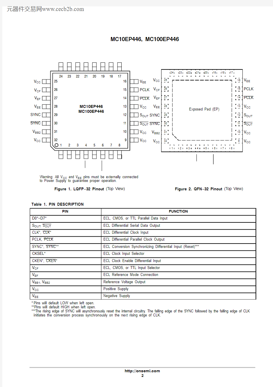
2526272829303132
1514
131211109
1
2345678
24
2322212019181716Figure 1. LQFP ?32 Pinout (Top View)Warning: All V CC and V EE pins must be externally connected to Power Supply to guarantee proper operation.
D 0
D 1
D 3
D 4
D 7
V CC S OUT V EE V BB2V C C
C K S E L
V EF V EE PCLK PCLK D 2
D 5
D 6
S OUT V CF SYNC SYNC V CC
C L K
C L K
V B B 1
C K E N
C K E N
V E E
V CC
V CC V CC
MC10EP446MC100EP446
Figure 2. QFN ?32 Pinout (Top View)
32
313029282726259
101112131415161
2
3
4
5
6
7
8
242322212019
18
17
Exposed Pad (EP)
D 0
D 1
D 3
D 4
D 7
V C C
C K S E L
D 2
D 5
D 6
C L K
C L K
V B B 1
C K E N
C K E N
V E E
S OUT V EE PCLK PCLK S OUT V CC V CC V CC
V CC V EE
V BB2V EF V CF SYNC SYNC V CC
Table 1. PIN DESCRIPTION
PIN
FUNCTION
D0*?D7*ECL, CMOS, or TTL Parallel Data Input S OUT , S OUT ECL Differential Serial Data Output CLK*, CLK*ECL Differential Clock Input
PCLK, PCLK ECL Differential Parallel Clock Output
SYNC*, SYNC**ECL Conversion Synchronizing Differential Input (Reset)***CKSEL*ECL Clock Input Selector
CKEN*, CKEN*ECL Clock Enable Differential Input V CF ECL, CMOS, or TTL Input Selector V EF ECL Reference Mode Connection V BB1, V BB2Reference Voltage Output V CC Positive Supply V EE
Negative Supply
*Pins will default LOW when left open.**Pins will default HIGH when left open.
***The rising edge of SYNC will asynchronously reset the internal circuitry. The falling edge of the SYNC followed by the falling edge of CLK initiates the conversion process synchronously on the next rising edge of CLK.
Table 2. TRUTH TABLE
the conversion process synchronously on the next rising edge of CLK.
Table 3. INPUT VOLTAGE LEVEL SELECTION TABLE Input Function Connect To V CF Pin
ECL Mode V EF Pin
CMOS Mode No Connect
TTL Mode* 1.5 V $ 100 mV
*For TTL Mode, if no external voltage can be provided, the reference voltage can be provided by connecting the appropriate resistor between V CF and V EE pins.Table 4. DATA INPUT OPERATING VOLTAGE TABLE Power Supply
(V CC,V EE)
Data Inputs (D [0:7])
CMOS TTL PECL NECL PECL p p p N/A
NECL N/A N/A N/A p
Power Supply Resistor Value 10% (Tolerance)
3.3 V 1.5 k W
5.0 V500 W
SYNC
Figure 3. Logic Diagram
CKEN CKEN CLK CLK CKSEL SYNC
V EE
V CC
Table 5. ATTRIBUTES
Characteristics Value Internal Input Pulldown Resistor75 k W Internal Input Pullup Resistor37.5 k W
ESD Protection Human Body Model
Machine Model
Charged Device Model > 2 kV > 100 V > 2 kV
Moisture Sensitivity, Indefinite Time Out of Drypack (Note 1)Pb Pkg Pb?Free Pkg
LQFP?32 QFN?32Level 2
?
Level 2
Level 1
Flammability Rating Oxygen Index: 28 to 34UL 94 V?0 @ 0.125 in
Transistor Count962 Devices
Meets or exceeds JEDEC Spec EIA/JESD78 IC Latchup Test
1.For additional information, see Application Note AND8003/D.
Table 6. MAXIMUM RATINGS
Symbol Parameter Condition 1Condition 2Rating Unit V CC PECL Mode Power Supply V EE = 0 V6V V EE NECL Mode Power Supply V CC = 0 V?6V
V I PECL Mode Input Voltage
NECL Mode Input Voltage V EE = 0 V
V CC = 0 V
V I≤ V CC
V I≥ V EE
6
?6
V
I out Output Current Continuous
Surge 50
100
mA
I BB V BB Sink/Source± 0.5mA T A Operating Temperature Range?40 to +85°C T stg Storage Temperature Range?65 to +150°C
q JA Thermal Resistance (Junction?to?Ambient)0 lfpm
500 lfpm LQFP?32
LQFP?32
80
55
°C/W
q JC Thermal Resistance (Junction?to?Case)Standard Board LQFP?3212 to 17°C/W
q JA Thermal Resistance (Junction?to?Ambient)0 lfpm
500 lfpm QFN?32
QFN?32
31
27
°C/W
q JC Thermal Resistance (Junction?to?Case)2S2P QFN?3212°C/W
T sol Wave Solder Pb
Pb?Free <2 to 3 sec @ 248°C
<2 to 3 sec @ 260°C
265
265
°C
Stresses exceeding Maximum Ratings may damage the device. Maximum Ratings are stress ratings only. Functional operation above the Recommended Operating Conditions is not implied. Extended exposure to stresses above the Recommended Operating Conditions may affect device reliability.
Table 7. 10EP DC CHARACTERISTICS, PECL V CC = 3.3 V, V EE = 0 V (Note 2)
Symbol Characteristic
?40°C25°C85°C
Unit Min Typ Max Min Typ Max Min Typ Max
I EE Power Supply Current901101409011014095115145mA V OH Output HIGH Voltage (Note 3)216522902415223023552480229024152540mV V OL Output LOW Voltage (Note 3)136514901615143015551680149016151740mV V IH Input HIGH Voltage (Single?Ended)
CMOS PECL
TTL 2000
2090
2000
3300
3300
3300
2000
2155
2000
3300
3300
3300
2000
2215
2000
3300
3300
3300
mV
V IL Input LOW Voltage (Single?Ended)
CMOS PECL
TTL
1365
800
1690
800
1460
800
1755
800
1490
800
1815
800
mV
V BB Output Voltage Reference179018401990185519052055191519652115mV V IHCMR Input HIGH Voltage Common Mode Range (Dif-
ferential Configuration) (Note 4)
2.0
3.3 2.0 3.3 2.0 3.3V
I IH Input HIGH Current150150150m A
I IL Input LOW Current(All Except SYNC, SYNC)
SYNC, SYNC
0.5
?1500.5
0.5
?1500.5
0.5
?1500.5
m A
NOTE:Device will meet the specifications after thermal equilibrium has been established when mounted in a test socket or printed circuit board with maintained transverse airflow greater than 500 lfpm. Electrical parameters are guaranteed only over the declared
operating temperature range. Functional operation of the device exceeding these conditions is not implied. Device specification limit values are applied individually under normal operating conditions and not valid simultaneously.
2.Input and output parameters vary 1:1 with V CC. V EE can vary +0.3 V to ?2.2 V.
3.All loading with 50 W to V CC? 2.0 V.
4.V IHCMR min varies 1:1 with V EE, V IHCMR max varies 1:1 with V CC. The V IHCMR range is referenced to the most positive side of the differential
input signal.
Table 8. 10EP DC CHARACTERISTICS, PECL V CC = 5.0 V, V EE = 0 V (Note 5)
Symbol Characteristic
?40°C25°C85°C
Unit Min Typ Max Min Typ Max Min Typ Max
I EE Power Supply Current901101409011014095115145mA V OH Output HIGH Voltage (Note 6)386539504115393040554180399041154240mV V OL Output LOW Voltage (Note 6)306531903315313032553380319033153440mV V IH Input HIGH Voltage (Single?Ended)
CMOS PECL
TTL 3500
3790
2000
5000
5000
5000
3500
3855
2000
5000
5000
5000
3500
3915
2000
5000
5000
5000
mV
V IL Input LOW Voltage (Single?Ended)
CMOS PECL
TTL
3065
1500
3390
800
3130
1500
3455
800
3190
1500
3915
800
mV
V BB Output Voltage Reference349035403690355536053755361536653815mV V IHCMR Input HIGH Voltage Common Mode Range (Dif-
ferential Configuration) (Note 7)
2.0 5.0 2.0 5.0 2.0 5.0V
I IH Input HIGH Current150150150m A
I IL Input LOW Current(All Except SYNC, SYNC)
SYNC, SYNC
0.5
?1500.5
0.5
?1500.5
0.5
?1500.5
m A
NOTE:Device will meet the specifications after thermal equilibrium has been established when mounted in a test socket or printed circuit board with maintained transverse airflow greater than 500 lfpm. Electrical parameters are guaranteed only over the declared
operating temperature range. Functional operation of the device exceeding these conditions is not implied. Device specification limit values are applied individually under normal operating conditions and not valid simultaneously.
5.Input and output parameters vary 1:1 with V CC. V EE can vary +2.0 V to ?0.5 V.
6.All loading with 50 W to V CC? 2.0 V.
7.V IHCMR min varies 1:1 with V EE, V IHCMR max varies 1:1 with V CC. The V IHCMR range is referenced to the most positive side of the differential
input signal.
Table 9. 10EP DC CHARACTERISTICS, NECL V CC = 0 V, V EE = ?5.5 V to ?3.0 V (Note 8)
Symbol Characteristic
?40°C25°C85°C
Unit Min Typ Max Min Typ Max Min Typ Max
I EE Power Supply Current901101409011014095115145mA V OH Output HIGH Voltage (Note 9)?1135?1010?885?1070?945?820?1010?885?760mV V OL Output LOW Voltage (Note 9)?1935?1810?1685?1870?1745?1620?1810?1685?1560mV V IH Input HIGH Voltage (Single?Ended)?1210?885?1145?820?1085?760mV V IL Input LOW Voltage (Single?Ended)?1935?1610?1870?1545?1810?1485mV V BB Output Voltage Reference?1510?1460?1310?1445?1395?1245?1385?1335?1185mV V IHCMR Input HIGH Voltage Common Mode
Range (Differential Configuration)
(Note 10)
V EE+2.00.0V EE+2.00.0V EE+2.00.0V
I IH Input HIGH Current150150150m A I IL Input LOW Current
(All Except SYNC, SYNC)
SYNC, SYNC
0.5
?1500.5
0.5
?1500.5
0.5
?1500.5
m A
NOTE:Device will meet the specifications after thermal equilibrium has been established when mounted in a test socket or printed circuit board with maintained transverse airflow greater than 500 lfpm. Electrical parameters are guaranteed only over the declared
operating temperature range. Functional operation of the device exceeding these conditions is not implied. Device specification limit values are applied individually under normal operating conditions and not valid simultaneously.
8.Input and output parameters vary 1:1 with V CC.
9.All loading with 50 W to V CC? 2.0 V.
10.V IHCMR min varies 1:1 with V EE, V IHCMR max varies 1:1 with V CC. The V IHCMR range is referenced to the most positive side of the differential
input signal.
Table 10. 100EP DC CHARACTERISTICS, PECL V CC = 3.3 V, V EE = 0 V (Note 11)
Symbol Characteristic
?40°C25°C85°C
Unit Min Typ Max Min Typ Max Min Typ Max
I EE Power Supply Current901101309011013095115135mA V OH Output HIGH Voltage (Note 12)215522802405215522802405215522802405mV V OL Output LOW Voltage (Note 12)135514801605135514801605135514801605mV V IH Input HIGH Voltage (Single?Ended)
CMOS PECL
TTL 2000
2075
2000
3300
3300
3300
2000
2075
2000
3300
3300
3300
2000
2075
2000
3300
3300
3300
mV
V IL Input LOW Voltage (Single?Ended)
CMOS PECL
TTL
1355
800
1675
800
1355
800
1675
800
1355
800
1675
800
mV
V BB Output Voltage Reference177518751975177518751975177518751975mV V IHCMR Input HIGH Voltage Common Mode
Range (Differential Configuration)
(Note 13)
2.0
3.3 2.0 3.3 2.0 3.3V
I IH Input HIGH Current150150150m A I IL Input LOW Current0.50.50.5m A NOTE:Device will meet the specifications after thermal equilibrium has been established when mounted in a test socket or printed circuit board with maintained transverse airflow greater than 500 lfpm. Electrical parameters are guaranteed only over the declared
operating temperature range. Functional operation of the device exceeding these conditions is not implied. Device specification limit values are applied individually under normal operating conditions and not valid simultaneously.
11.Input and output parameters vary 1:1 with V CC. V EE can vary +0.3 V to ?2.2 V.
12.All loading with 50 W to V CC? 2.0 V.
13.V IHCMR min varies 1:1 with V EE, V IHCMR max varies 1:1 with V CC. The V IHCMR range is referenced to the most positive side of the differential
input signal.
Table 11. 100EP DC CHARACTERISTICS, PECL V CC = 5.0 V, V EE = 0 V (Note 14)
Symbol Characteristic
?40°C25°C85°C
Unit Min Typ Max Min Typ Max Min Typ Max
I EE Power Supply Current901101309011013095115135mA V OH Output HIGH Voltage (Note 15)385539804105385539804105385539804105mV V OL Output LOW Voltage (Note 15)305531803305305531803305305531803305mV V IH Input HIGH Voltage (Single?Ended)
CMOS PECL
TTL 3500
3775
2000
5000
5000
5000
3500
3775
2000
5000
5000
5000
3500
3775
2000
5000
5000
5000
mV
V IL Input LOW Voltage (Single?Ended)
CMOS PECL
TTL
3055
1500
3375
800
3055
1500
3375
800
3055
1500
3375
800
mV
V BB Output Voltage Reference347535753675347535753675347535753675mV V IHCMR Input HIGH Voltage Common Mode
Range (Differential Configuration)
(Note 16)
2.0 5.0 2.0 5.0 2.0 5.0V
I IH Input HIGH Current150150150m A I IL Input LOW Current0.50.50.5m A NOTE:Device will meet the specifications after thermal equilibrium has been established when mounted in a test socket or printed circuit board with maintained transverse airflow greater than 500 lfpm. Electrical parameters are guaranteed only over the declared
operating temperature range. Functional operation of the device exceeding these conditions is not implied. Device specification limit values are applied individually under normal operating conditions and not valid simultaneously.
14.Input and output parameters vary 1:1 with V CC. V EE can vary +2.0 V to ?0.5 V.
15.All loading with 50 W to V CC? 2.0 V.
16.V IHCMR min varies 1:1 with V EE, V IHCMR max varies 1:1 with V CC. The V IHCMR range is referenced to the most positive side of the differential
input signal.
Table 12. 100EP DC CHARACTERISTICS, NECL V CC = 0 V, V EE = ?5.5 V to ?3.0 V (Note 17)
Symbol Characteristic
?40°C25°C85°C
Unit Min Typ Max Min Typ Max Min Typ Max
I EE Power Supply Current901101309011013095115135mA V OH Output HIGH Voltage (Note 18)?1145?1020?895?1145?1020?895?1145?1020?895mV V OL Output LOW Voltage (Note 18)?1945?1820?1695?1945?1820?1695?1945?1820?1695mV V IH Input HIGH Voltage (Single?Ended)?1225?880?1225?880?1225?880mV V IL Input LOW Voltage (Single?Ended)?1945?1625?1945?1625?1945?1625mV V BB Output Voltage Reference?1525?1425?1325?1525?1425?1325?1525?1425?1325mV V IHCMR Input HIGH Voltage Common Mode
Range (Differential Configuration)
(Note 19)
V EE+2.00.0V EE+2.00.0V EE+2.00.0V
I IH Input HIGH Current150150150m A I IL Input LOW Current0.50.50.5m A NOTE:Device will meet the specifications after thermal equilibrium has been established when mounted in a test socket or printed circuit board with maintained transverse airflow greater than 500 lfpm. Electrical parameters are guaranteed only over the declared
operating temperature range. Functional operation of the device exceeding these conditions is not implied. Device specification limit values are applied individually under normal operating conditions and not valid simultaneously.
17.Input and output parameters vary 1:1 with V CC.
18.All loading with 50 W to V CC? 2.0 V.
19.V IHCMR min varies 1:1 with V EE, V IHCMR max varies 1:1 with V CC. The V IHCMR range is referenced to the most positive side of the differential
input signal.
Table 13. AC CHARACTERISTICS V CC = 0 V; V EE = ?3.0 V to ?5.5 V or V CC = 3.0 V to 5.5 V; V EE = 0 V (Note 20)
Symbol Characteristic
?40°C
25°C 85°C Unit
Min
Typ
Max
Min
Typ
Max
Min
Typ
Max
f max
Maximum Frequency (Figure 15)
CKSEL High CKSEL Low
3.21.6 3.41.7 3.21.6 3.41.7 3.21.6 3.41.7GHz
t PLH ,t PHL
Propagation Delay to Output Differential CKSEL = 0CLK TO S OUT ,
CLK TO PCLK 6507007508008509007007508008509009507257758509009751025ps CKSEL = 1
CLK TO S OUT ,CLK TO PCLK
775850
875950
9751050
825900925100010251100
8759501000107511251200
ps
t S
Setup Time D to CLK+ (Figure 4)SYNC ? to CLK ? (Figure 5)CKEN+ to CLK ? (Figure 6)?37520070?42514040?40020070?45014040?45020070?50014040ps
t h
Hold Time D to CLK+(Figure 4)SYNC ? to CLK ?
CLK ? to CKEN ? (Figure 6)?525075?575
45?550075?60045
?600075?65045
ps
t pw
Minimum Pulse Width (Note 22)Data (D0?D7)SYNC CKEN
150200145
150200145
150200145
ps
t JITTER Random Clock Jitter (RMS)v f max Typ
0.2
< 10.2< 10.2< 1ps V PP Input Differential Voltage Swing (Note 21)
150
800120015080012001508001200mV t r t f
Output Rise/Fall Times S OUT
(20% ? 80%)
50
100
150
70
120
170
90
140
190
ps
NOTE:Device will meet the specifications after thermal equilibrium has been established when mounted in a test socket or printed circuit
board with maintained transverse airflow greater than 500 lfpm. Electrical parameters are guaranteed only over the declared
operating temperature range. Functional operation of the device exceeding these conditions is not implied. Device specification limit values are applied individually under normal operating conditions and not valid simultaneously.
20.Measured using a 750 mV source, 50% duty cycle clock source. All loading with 50 W to V CC ? 2.0 V.21.V PP (min) is the minimum input swing for which AC parameters are guaranteed.22.The minimum pulse width is valid only if the setup and hold times are respected.
CLK
SYNC SYNC
CLK
CLK
CKEN
Figure 4. Setup and Hold Time for Data
Data Setup Time
+ 0 ?
CLK
Figure 5. Setup Time for SYNC Figure 6. Setup and Hold Time for CKEN
APPLICATION INFORMATION
The MC10/100EP446 is an integrated 8:1 parallel to serial converter. An attribute for EP446 is that the parallel inputs D0–D7 (Pins 17 – 24) can be configured to accept either CMOS, ECL, or TTL level signals by a combination of interconnects between V EF (Pin 27) and V CF (Pin 26) pins.For CMOS input levels, leave V EF and V CF open. For ECL operation, short V CF and V EF (Pins 26 and 27). For TTL operation, connect a 1.5 V supply reference to V CF and leave the V EF pin open. The 1.5 V reference voltage to V CF pin can be accomplished by placing a 1.5 k W or 500 W between V CF and V EE for 3.3 V or 5.0 V power supplies, respectively.
Note: all pins requiring ECL voltage inputs must have a 50 W terminating resistor to V TT (V TT = V CC – 2.0 V).The CKSEL input (Pin 2) is provided to enable the user to select the serial data rate output between internal clock data rate or twice the internal clock data rate. For CKSEL LOW operation, the time from when the parallel data is latched ?to when the data is seen on the S OUT - is on the falling edge of the 7th clock cycle plus internal propagation delay (Figure 7). Note the PCLK switches on the falling edge of CLK.
Figure 7. Timing Diagram 1:8 Parallel to Serial Conversion with CKSEL LOW
CLK SOUT PCLK
D0D0?2D1D2D3D4D5D6D7
D2?2D3?2D4?2D5?2D6?2D7?2
D0?3D1?3D2?3D3?3D4?3D5?3D6?3D7?3
D1?2CKSEL D 0?1
D 1?1
D 2?1
D 3?1
D 4?1
D 5?1
D 6?1
D 7?1
D 0?2
D 1?2
D 2?2
D 3?2
D 6?2
D0?1D2?1D3?1D4?1D5?1D6?1D7?1
D1?1D 5?2
D0?4D1?4D2?4D3?4D4?4D5?4D6?4D7?4
1234567
Number of Clock Cycles from Data Latch to SOUT Data Latched
Data Latched
Data Latched Data Latched D 4?2
à
á
Similarly, for CKSEL HIGH operation, the time from when the parallel data is latched ? to when the data is seen on the S OUT - is on the rising edge of the 14th clock cycle plus internal propagation delay (Figure 8). Furthermore, the PCLK switches on the rising edge of CLK.
Data Latched
Data Latched
Data Latched Figure 8. Timing Diagram 1:8 Parallel to Serial Conversion with CKSEL HIGH
CLK SOUT PCLK
D0D0?1D1D2D3D4D5D6D7
D2?1D3?1D4?1D5?1D6?1D7?1
D1?1CKSEL D0?2D1?2D2?2D3?2D4?2D5?2D6?2D7?2
D0?3D1?3D2?3D3?3D4?3D5?3D6?3D7?3
D 0?1
D 1?1
D 2?1
D 3?1
D 4?1
D 5?1
D 6?1
D 7?1
D 0?2
D 1?2
1
2
3
4
5
6
7
8
9
10
12
13
14
11
à
á
Number of Clock Cycles from Data Latch to SOUT
The device also features a differential SYNC input (Pins 29 and 30), which asynchronously reset all internal flip–flops and clock circuitry on the rising edge of SYNC. The release of SYNC is a synchronous process, which ensures that no runt serial data bits are generated. The falling edge of the SYNC followed by a falling edge of CLK initiates the start of the conversion process on the next rising edge of CLK (Figures 9 and 10). As shown in the figures below, the device will start to latch the parallel input data after the a falling edge of SYNC ?, followed by the falling edge CLK -, on the next rising of edge of CLK ? for CKSEL LOW
Figure 9. Timing Diagram 1:8 Parallel to Serial Conversion with CKSEL LOW and SYNC
CLK SYNC SOUT PCLK
D0
D1D2D3D4D5D6D7
CKSEL Figure 10. Synchronous Release of SYNC for CKSEL LOW
CLK
SYNC
SYNC
(Synchronous ENABLE)
For CKSEL HIGH, as shown in the timing diagrams below, the device will start to latch the parallel input data after the falling edge of SYNC ?, followed by the falling edge CLK -, on the second rising edge of CLK ? (Figures 11 and 12).
CLK SYNC SOUT PCLK
D0D1D2D3D4D5D6D7
CKSEL Figure 12. Synchronous Release of SYNC for CKSEL HIGH
SYNC
(Synchronous ENABLE)
The differential synchronous CKEN inputs (Pins 6 and 7), disable the internal clock circuitry. The synchronous CKEN will suspend all of the device activities and prevent runt pulses from being generated. The rising edge of CKEN followed by the falling edge of CLK will suspend all activities. The falling edge of CKEN followed by the falling edge of CLK will resume all activities (Figure 13).
Figure 13. Timing Diagram with CKEN with CKSEL HIGH
CLK CKEN SOUT CKSEL
PCLK Internal Clock Disabled
Internal Clock Enabled
The differential PCLK output (Pins 14 and 15) is a word framer and can help the user synchronize the serial data output, S OUT (Pins 11 and 12), in their applications.Furthermore, PCLK can be used as a trigger for input parallel data (Figure 14).
An internally generated voltage supply, the V BB pin, is available to this device only. For single–ended input
conditions, the unused differential input is connected to V BB as a switching reference voltage. V BB may also rebias AC coupled inputs. When used, decouple V BB and V CC via a 0.01 m F capacitor and limit current sourcing or sinking to 0.5 mA. When not used, V BB should be left open. Also, both outputs of the differential pair must be terminated (50 W to V TT ) even if only one output is used.
Figure 14. PCLK as Trigger Application
CLK
RESET
0500100015002000250030003500
INPUT CLOCK FREQUENCY (MHz)
Figure 15. Typical V OUTPP versus Input Clock Frequency, 255C
(Condition: 3.4 GHz input frequency, CKSEL HIGH, BEOFE32 bit pattern on SOUT
Figure 17. Typical Termination for Output Driver and Device Evaluation (See Application Note AND8020/D ? Termination of ECL Logic Devices.)
V TT
V TT = V CC ? 2.0 V
ORDERING INFORMATION
Device
Package Shipping ?MC10EP446FA LQFP ?32250 Units / Tray MC10EP446FAG LQFP ?32(Pb ?Free)250 Units / Tray MC10EP446FAR2LQFP ?322000 / Tape & Reel MC10EP446FAR2G LQFP ?32(Pb ?Free)2000 / Tape & Reel MC100EP446FA LQFP ?32250 Units / Tray MC100EP446FAG LQFP ?32(Pb ?Free)250 Units / Tray MC100EP446FAR2LQFP ?322000 / Tape & Reel MC100EP446FAR2G LQFP ?32(Pb ?Free)2000 / Tape & Reel MC10EP446MNG QFN ?32(Pb ?Free)74 Units / Rail MC100EP446MNG QFN ?32(Pb ?Free)74 Units / Rail MC10EP446MNR4G QFN ?32(Pb ?Free)1000 / Tape & Reel MC100EP446MNR4G
QFN ?32(Pb ?Free)
1000 / Tape & Reel
?For information on tape and reel specifications, including part orientation and tape sizes, please refer to our Tape and Reel Packaging Specifications Brochure, BRD8011/D.
Resource Reference of Application Notes
AN1405/D ?ECL Clock Distribution Techniques AN1406/D ?Designing with PECL (ECL at +5.0 V)AN1503/D ?ECLinPS t I/O SPiCE Modeling Kit AN1504/D ?Metastability and the ECLinPS Family AN1568/D ?Interfacing Between LVDS and ECL AN1672/D ?The ECL Translator Guide AND8001/D ?Odd Number Counters Design AND8002/D ?Marking and Date Codes AND8020/D ?Termination of ECL Logic Devices AND8066/D ?Interfacing with ECLinPS
AND8090/D
?AC Characteristics of ECL Devices
PACKAGE DIMENSIONS
AE
T ?U M
0.20 (0.008)
Z
A C 32 LEAD LQFP CASE 873A ?02NOTES:
1.DIMENSIONING AND TOLERANCING PER ANSI Y14.5M, 198
2.
2.CONTROLLING DIMENSION:MILLIMETER.
3.DATUM PLANE ?AB ? IS LOCATED AT BOTTOM OF LEAD AND IS COINCIDENT WITH THE LEAD WHERE THE LEAD EXITS THE PLASTIC BODY AT THE BOTTOM OF THE PARTING LINE.
4.DATUMS ?T ?, ?U ?, AND ?Z ? TO BE DETERMINED AT DATUM PLANE ?AB ?.
5.DIMENSIONS S AND V TO BE
DETERMINED AT SEATING PLANE ?AC ?.6.DIMENSIONS A AND B DO NOT INCLUDE MOLD PROTRUSION.
ALLOWABLE PROTRUSION IS 0.250(0.010) PER SIDE. DIMENSIONS A AND B DO INCLUDE MOLD MISMATCH AND ARE DETERMINED AT DATUM PLANE ?AB ?.
7.DIMENSION D DOES NOT INCLUDE DAMBAR PROTRUSION. DAMBAR
PROTRUSION SHALL NOT CAUSE THE D DIMENSION TO EXCEED 0.520 (0.020).8.MINIMUM SOLDER PLATE THICKNESS SHALL BE 0.0076 (0.0003).
9.EXACT SHAPE OF EACH CORNER MAY VARY FROM DEPICTION.
DIM A MIN MAX MIN MAX INCHES 7.000 BSC 0.276 BSC MILLIMETERS B 7.000 BSC 0.276 BSC C 1.400 1.6000.0550.063D 0.3000.4500.0120.018E 1.350 1.4500.0530.057F 0.3000.4000.0120.016G 0.800 BSC 0.031 BSC H 0.0500.1500.0020.006J 0.0900.2000.0040.008K 0.4500.750
0.0180.030
M 12 REF 12 REF N 0.0900.1600.0040.006P 0.400 BSC 0.016 BSC Q 1 5 1 5 R 0.1500.2500.0060.010V 9.000 BSC 0.354 BSC V1 4.500 BSC 0.177 BSC ______B1 3.500 BSC 0.138 BSC A1 3.500 BSC 0.138 BSC S 9.000 BSC 0.354 BSC S1 4.500 BSC 0.177 BSC W 0.200 REF 0.008 REF X
1.000 REF 0.039 REF
PACKAGE DIMENSIONS
QFN32 5*5*1 0.5 P CASE 488AM ?01
2 X
*For additional information on our Pb ?Free strategy and soldering details, please download the ON Semiconductor Soldering and Mounting Techniques Reference Manual, SOLDERRM/D.
ON Semiconductor and are registered trademarks of Semiconductor Components Industries, LLC (SCILLC). SCILLC reserves the right to make changes without further notice to any products herein. SCILLC makes no warranty, representation or guarantee regarding the suitability of its products for any particular purpose, nor does SCILLC assume any liability arising out of the application or use of any product or circuit, and specifically disclaims any and all liability, including without limitation special, consequential or incidental damages.“Typical” parameters which may be provided in SCILLC data sheets and/or specifications can and do vary in different applications and actual performance may vary over time. All operating parameters, including “Typicals” must be validated for each customer application by customer’s technical experts. SCILLC does not convey any license under its patent rights nor the rights of others. SCILLC products are not designed, intended, or authorized for use as components in systems intended for surgical implant into the body, or other applications intended to support or sustain life, or for any other application in which the failure of the SCILLC product could create a situation where personal injury or death may occur. Should Buyer purchase or use SCILLC products for any such unintended or unauthorized application, Buyer shall indemnify and hold SCILLC and its officers, employees, subsidiaries, affiliates,and distributors harmless against all claims, costs, damages, and expenses, and reasonable attorney fees arising out of, directly or indirectly, any claim of personal injury or death associated with such unintended or unauthorized use, even if such claim alleges that SCILLC was negligent regarding the design or manufacture of the part. SCILLC is an Equal Opportunity/Affirmative Action Employer. This literature is subject to all applicable copyright laws and is not for resale in any manner.
PUBLICATION ORDERING INFORMATION
ECLinPS is a trademark of Semiconductor Components INdustries, LLC (SCILLC).