ACA0861 - A, B, C, D
750/860 MHz CATV Line Amplifier MMIC
Data Sheet - Rev 2.2
PRODUCT DESCRIPTION
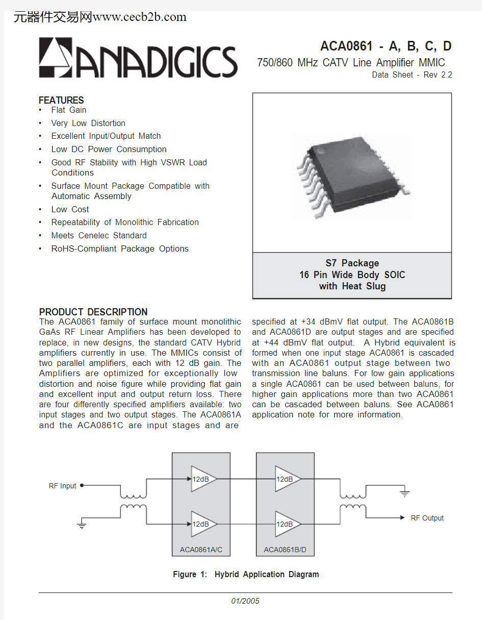
The ACA0861 family of surface mount monolithic GaAs RF Linear Amplifiers has been developed to replace, in new designs, the standard CATV Hybrid amplifiers currently in use. The MMICs consist of two parallel amplifiers, each with 12 dB gain. The Amplifiers are optimized for exceptionally low distortion and noise figure while providing flat gain and excellent input and output return loss. There are four differently specified amplifiers available: two input stages and two output stages. The ACA0861A and the ACA0861C are input stages and are
specified at +34 dBmV flat output. The ACA0861B and ACA0861D are output stages and are specified at +44 dBmV flat output. A Hybrid equivalent is formed when one input stage ACA0861 is cascaded with an ACA0861 output stage between two transmission line baluns. For low gain applications a single ACA0861 can be used between baluns, for higher gain applications more than two ACA0861can be cascaded between baluns. See ACA0861application note for more information.
FEATURES
?Flat Gain
?Very Low Distortion
?Excellent Input/Output Match ?Low DC Power Consumption
?Good RF Stability with High VSWR Load Conditions
?Surface Mount Package Compatible with Automatic Assembly ?Low Cost
?Repeatability of Monolithic Fabrication ?Meets Cenelec Standard
?
RoHS-Compliant Package Options
Figure 1: Hybrid Application Diagram
RF
Output
元器件交易网https://www.doczj.com/doc/c814233268.html,
ACA0861 - A, B, C, D
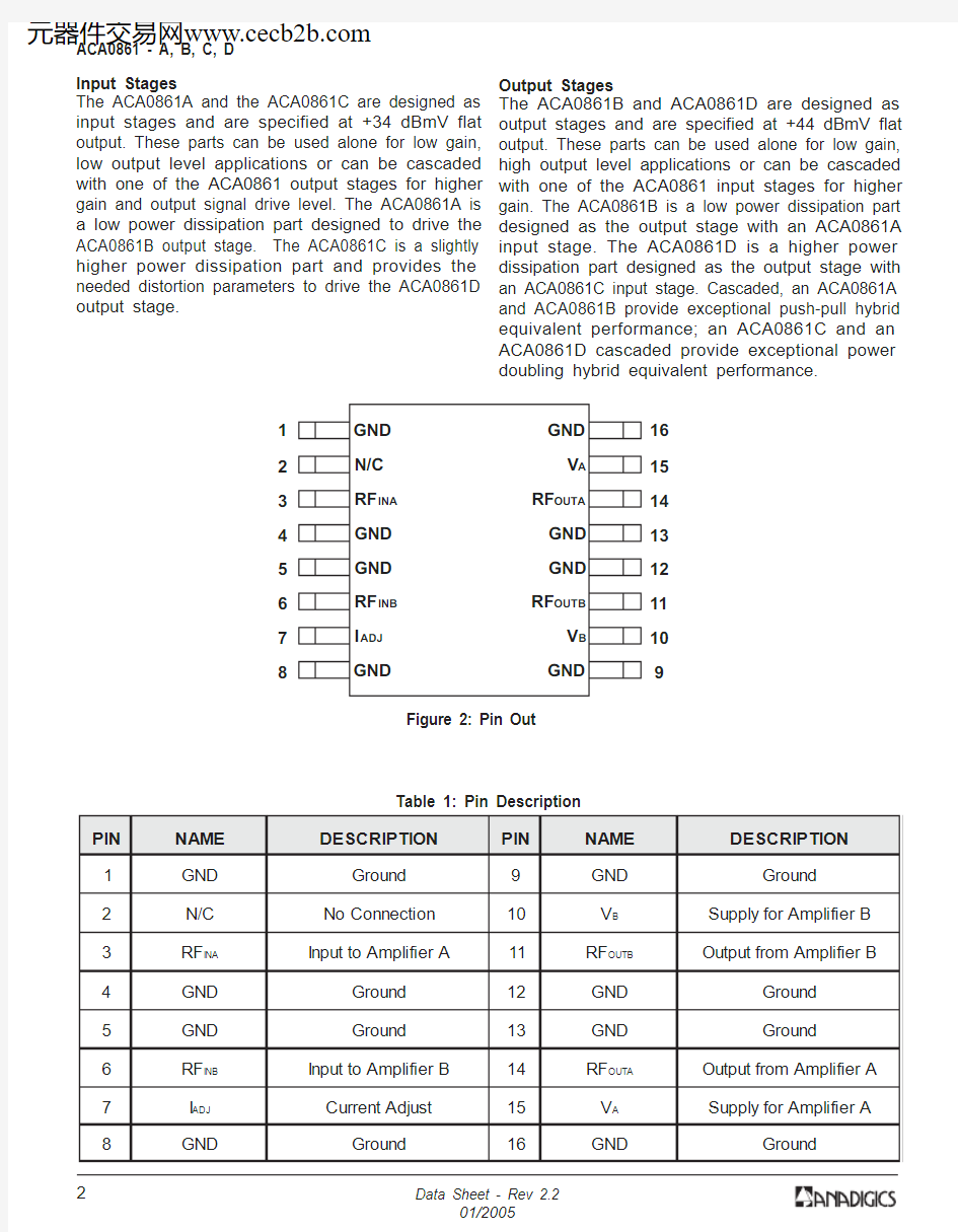
Figure 2: Pin Out
Table 1: Pin Description
Input Stages
The ACA0861A and the ACA0861C are designed as input stages and are specified at +34 dBmV flat output. These parts can be used alone for low gain,low output level applications or can be cascaded with one of the ACA0861 output stages for higher gain and output signal drive level. The ACA0861A is a low power dissipation part designed to drive the ACA0861B output stage. The ACA0861C is a slightly higher power dissipation part and provides the needed distortion parameters to drive the ACA0861D output stage.
Output Stages
The ACA0861B and ACA0861D are designed as output stages and are specified at +44 dBmV flat output. These parts can be used alone for low gain,high output level applications or can be cascaded with one of the ACA0861 input stages for higher gain. The ACA0861B is a low power dissipation part designed as the output stage with an ACA0861A input stage. The ACA0861D is a higher power dissipation part designed as the output stage with an ACA0861C input stage. Cascaded, an ACA0861A and ACA0861B provide exceptional push-pull hybrid equivalent performance; an ACA0861C and an ACA0861D cascaded provide exceptional power doubling hybrid equivalent performance.
12345678
161514131211109
元器件交易网https://www.doczj.com/doc/c814233268.html,
ACA0861 - A, B, C, D
ELECTRICAL CHARACTERISTICS
Table 2: Absolute Minimum and Maximum Ratings
damage. Functional operation is not implied under these conditions.Exposure to absolute ratings for extended periods of time may adversely affect reliability.Table 3: Operating Ranges
performance is guaranteed only over the conditions defined in the electrical specifications.
Notes:
1. Pins 3 and 6 should be AC-coupled. No external DC bias should be applied.
2. Pin 7 should be pulled to ground through a resistor or left open-circuited.No external DC bias should be applied.
元器件交易网https://www.doczj.com/doc/c814233268.html,
元器件交易网https://www.doczj.com/doc/c814233268.html,
ACA0861 - A, B, C, D
Table 4: Electrical Specifications
(T A = +25 °C, V D = +12 VDC)
Notes:
(1) Measured performance of MMIC alone. Balun effects de-imbedded from measurement.
(2) Measured with a balun on input and output of the device. See Figure 3 for test setup.
(3) All parts measured with 110 channel flat input. Parts A and C measured at +34 dBmV output (per channel).
Parts B and D measured at +44 dBmV output (per channel).
(4) A fixed resistor is needed for parts A through C; part D does not need an external resistor (see Table 6.)
These resistors set the devices’ current draw. Bias voltage is +12 VDC.
ACA0861 - A, B, C, D
Note: Apply voltage to both V D lines simultaneously.
Figure 3: Test Circuit Table 5: Parts List for Test Circuit
(1) T1, T2 (balun) wind 4 turns thru core, as shown in Figure 4.
RF 元器件交易网https://www.doczj.com/doc/c814233268.html,
ACA0861 - A, B, C, D
PERFORMANCE DATA
100
200
300
400
500
600
700
800
900
1000
Frequency (MHz)
S 21(d B )
Figure 5:Gain /S21
Figure 6:Reverse Isolation /
S12
100
200
300
400
500
600
700
800
900
1000
Frequency (MHz)
S 12(d B )
Figure 7:Input Return Loss /S11
400
100
200
300
500
600
700
800
900
1000
Frequency (MHz)
S 11(d B
)
Figure 8:Noise Figure vs.
Frequency
Frequency (MHz)
N F
(d B )
Figure 9:Output Return Loss /
S22
-45.0
-40.0-35.0-30.0-25.0-20.0-15.0-10.0
-5.00.05.00
100
200
300
400
500
600
700
800
900
1000
Frequency (MHz)
S 22(d B
)
ACA0861A and ACA0861B Cascade Typical Data (see Figure 42)元器件交易网https://www.doczj.com/doc/c814233268.html,
ACA0861 - A, B, C, D
Figure 10:CTB (77Channel Loading,
Flat)
-90
-85-80-75-70-65-60-55-50-45-400
100
200
300
400
500
600
Frequency (MHz)
C T B (d B c )
Output Power (dBmV)
Figure 11:CSO (77Channel Loading,
Flat)
-90
-85-80-75-70-65-60
-55-500
100
200
300
400
500
600
Frequency (MHz)
C S O (d B c )
Output Power (dBmV)
-70
-65-60-55-50-45-40-35-300
100
200
300
400
500
600
X m o d (d B c )
Output Power (dBmV)
ACA0861A and ACA0861B Cascade Typical Data (see Figure 42)
元器件交易网https://www.doczj.com/doc/c814233268.html,
ACA0861 - A, B, C, D
-90
-85-80-75-70-65-60-55-50-45-400
100
200
300
400
500
600
700
800
Frequency (MHz)
C T B (d B c )
Output
Power
(dBmV)
-90
-85-80-75-70-65-60-55-500
100200300400500600700800
Frequency (MHz)
C S O (d B c )
Output Power (dBmV)
Figure 15:XMOD (110Channel Loading,
Flat)
-70
-65-60-55-50-45-40-35-300
100
200
300
400
500
600
700
800
X m o d (d B c )
Output Power (dBmV)
ACA0861A and ACA0861B Cascade Typical Data (see Figure 42)
元器件交易网https://www.doczj.com/doc/c814233268.html,
ACA0861 - A, B, C, D
-90
-85-80-75-70-65-60-55-50-45-400
200
400600800
1000
Frequency (MHz)
C T B (d B c )
Output Power (dBmV)
-90
-85-80-75-70-65-60
-55-500
200
400
600
800
1000
Frequency (MHz)
C S O (d B c )
Output Power
(dBmV)
-70
-65-60-55-50-45-40
-35-300
200
400
600
800
1000
X m o d (d B c )
Output Power (dBmV)
ACA0861A and ACA0861B Cascade Typical Data (see Figure 42)
元器件交易网https://www.doczj.com/doc/c814233268.html,
ACA0861 - A, B, C, D
Figure 19:Gain /
S21
100
200
300
400
500
600
700
800
900
1000
Frequency (MHz)
S 21(d B )
Figure 20:Reverse Isolation /S12
Frequency (MHz)
S 12(d B )
Frequency (MHz)
S 11(d B )
0.53.5
4.5Frequency (MHz)
N F (d
B )
S 22(d B )
ACA0861C and ACA0861D Cascade Typical Data (see Figure 42)元器件交易网https://www.doczj.com/doc/c814233268.html,
ACA0861 - A, B, C, D
-90
-85-80-75-70-65-60-55-50-45-400
100
200
300400
500
600
Frequency (MHz)
C T B (d B c )
Output Power (dBmV)
-90
-85-80-75-70-65-60
-55-500
100
200
300400
500
600
Frequency (MHz)
C S O (d B c )
Output Power (dBmV)
-90
-85-80-75-70-65-60
-55-500
100
200
300
400
500
600
700
800
Frequency (MHz)
C S O (d B c )
Output Power (dBmV)
Figure 28:XMOD (77Channel Loading,
Flat)
-90
-85-80-75-70-65-60-55-50-45-400
100
200
300400
500
600
Frequency (MHz)
X m o d (d B c )
Output Power
(dBmV)
Figure 29:XMOD (110Channel Loading,
Flat)
-90
-85-80-75-70-65-60-55-50-45-400
100
200
300
400
500
600
700
800
Frequency (MHz)
X m o d (d B c )
Output Power (dBmV)
Figure 25:CTB (110Channel Loading,
Flat)
-90
-85-80-75-70-65-60-55
-50-45-400
100
200
300
400
500
600
700
800
Frequency (MHz)
C T B (d B c )
Output Power (dBmV)
ACA0861C and ACA0861D Cascade Typical Data (see Figure 42)
元器件交易网https://www.doczj.com/doc/c814233268.html,
ACA0861 - A, B, C, D
Figure 30:CTB (128Channel Loading,
Flat)
-90
-85-80-75-70-65-60-55-50-45-400
200
400
600
800
1000
Frequency (MHz)
C T B (d B c )
Output
Power (dBmV)
Figure 31:CTB (77Channel Loading,8dB
Tilt)
-90
-85-80-75-70-65-60-55-50-45-400
100
200
300
400
500
600
Frequency (MHz)
C T B (d B c )
Output Power Figure 32:CSO (128Channel Loading,
Flat)
-90
-85-80-75-70-65-60
-55-500
200
400
600
800
1000
Frequency (MHz)
C S O (d B c )
Output Power Figure 33:CSO (77Channel Loading,8dB
Tilt)
-90
-85-80-75-70-65-60-55-500
100
200
300
400
500
600
Frequency (MHz)
C S O (d B c )
Output Power Figure 34:XMOD (128Channel Loading,
Flat)
-90
-85-80-75-70-65-60-55
-50-45-400
200
400
600
800
1000
Frequency (MHz)
X m
o d (d B c )
Output Power
Tilt)
-90
-85-80-75-70-65-60-55-50-45-400100200300
400500600
Frequency (MHz)
X m o d (d B c )
Output Power ACA0861C and ACA0861D Cascade Typical Data (see Figure 42)
元器件交易网https://www.doczj.com/doc/c814233268.html,
ACA0861 - A, B, C, D
Figure 36:CTB (110Channel Loading,10dB
Tilt)
-90
-85-80-75-70-65-60-55-50-45-400
100
200
300
400
500
600
700
800
Frequency (MHz)
C T B (d B c )
Output Power Figure 37:CTB (128Channel Loading,12dB
Tilt)
-90
-85-80-75-70-65-60-55-50-45-400
200
400
600
800
1000
Frequency (MHz)
C T B (d B c )
Output Power (dBmV)
Figure 38:CSO (110Channel Loading,10dB
Tilt)
-90
-85-80-75-70-65-60-55-500
100
200
300
400
500
600
700
800
Frequency (MHz)
C S O (d B c )
Output Power Figure 39:CSO (128Channel Loading,12dB
Tilt)
-90
-85-80-75-70-65-60-55-500
200
400
600
800
1000
Frequency (MHz)
C S O (d B c
)
Output Power (dBmV)
Figure 40:XMOD (110Channel Loading,10dB
Tilt)-90
-85-80-75-70-65-60-55-50-45-400
100
200
300
400
500
600
700
800
Frequency (MHz)
X m o d (d B c
)
Output Power (dBmV)
Tilt)
-90
-85-80-75-70-65-60-55
-50-45-400
200
400
600
800
1000
Frequency (MHz)
X m o d (d B c )
Output Power (dBmV)
ACA0861C and ACA0861D Cascade Typical Data (see Figure 42)
元器件交易网https://www.doczj.com/doc/c814233268.html,
ACA0861 - A, B, C, D
APPLICATION INFORMATION
Figure 42: Hybrid Equivalent Test Circuit
Notes:
1. Apply voltage to all +12 Vdc lines simultaneously.
2. See Table 6 for R1 values.
3. Input and output baluns: wind 5 turns thru core (see Table 7), as shown in Figure 43.
Table 7: Parts List for Balun (5 Turns)
元器件交易网https://www.doczj.com/doc/c814233268.html,
元器件交易网https://www.doczj.com/doc/c814233268.html,
ACA0861 - A, B, C, D
PACKAGE OUTLINE Array Figure 44: S7 Package Outline - 16 Pin Wide Body SOIC with Heat Slug
WARNING
ANADIGICS products are not intended for use in life support appliances, devices or systems. Use of an ANADIGICS IMPORTANT NOTICE
ANADIGICS, Inc.
141 Mount Bethel Road
Warren, New Jersey 07059, U.S.A.Tel: +1 (908) 668-5000Fax: +1 (908) 668-5132URL: https://www.doczj.com/doc/c814233268.html, E-mail: Mktg@https://www.doczj.com/doc/c814233268.html,
ANADIGICS, Inc. reserves the right to make changes to its products or to discontinue any product at any time without notice. The product specifications contained in Advanced Product Information sheets and Preliminary Data Sheets are subject to change prior to a product’s formal introduction. Information in Data Sheets have been carefully checked and are assumed to be reliable; however, ANADIGICS assumes no responsibilities for inaccuracies. ANADIGICS strongly urges customers to verify that the information they are using is current before placing orders.
ACA0861 - A, B, C, D
ORDERING INFORMATION
元器件交易网https://www.doczj.com/doc/c814233268.html,