Active-matrix organic light-emitting diode using inverse-staggered poly-Si TFTs with a center-offset gated structure
Dong Han Kang(SID Student Member) Mi Kyung Park
Jin Jang(SID Fellow)
Young Jin Chang
Jae Hwan Oh
Jae Beom Choi
Chi Woo Kim Abstract—A low-cost active-matrix backplane using non-laser polycrystalline silicon(poly-Si)having inverse-staggered TFTs with amorphous-silicon(a-Si)n+contacts has been developed.The thin-film transistors(TFTs)have a center-offset gated structure to reduce the leakage current without scarifying the ON-currents.The leakage current of the center-offset TFTs at V g=–10V is two orders of magnitude lower than those of the non-offset TFTs.The center-offset length of the TFTs was3μm for both the switching and driving TFTs.A2.2-in.QQVGA(160×120) active-matrix organic light-emitting-diode (AMOLED)display was demonstrated using conventional2T+1C pixel circuits. Keywords—Poly-Si,LTPS TFT,bottom-gate TFT,leaksgae current,center offset, AMOLED.
DOI#10.1889/JSID18.2.122
1Introduction
Polycrystalline silicon(poly-Si)on glass is an attractive material for large-area electronics such as active-matrix displays.1 But its manufacturing cost is higher than that of hydrogen-ated amorphous-silicon(a-Si:H)based technology;thus,a new low-cost poly-Si thin-film-transistor(TFT)device and process are needed.One of the most promising methods is the use of both non-laser crystallization of a-Si:H and an inverse-staggered structure to compete with a-Si:H back-plane technology.2
Recently,much attention has been given to the inverse-staggered poly-Si TFT,fabricated by using either laser or non-laser-based low-temperature poly-Si(LTPS).3,4The advantage of the inverse-staggered device is that the device structure and fabrication process are almost identical to those of a-Si:H TFTs used for the manufacture of current TFT-LCDs.The existing a-Si:H production line can be easily modified to the LTPS line,with the addition of the equip-ment required for the crystallization process,such as cap-ping layer deposition,Ni deposition,and SiN x removal process after annealing.
On the other hand,conventional poly-Si TFTs suffer from relatively high leakage currents compared to that of a-Si TFTs.5This is a serious problem for pixel switches in AMOLEDs.Various lightly doped drain(LDD)and offset gated structures have been adopted to suppress the leakage currents by reducing electric field near the drain electrode.6 However,the ON-currents of LDD and offset TFTs are less than those of self-aligned TFTs due to the high series resis-tance of the offset(LDD)region if it is longer,and also an additional process step is needed to make the LDD region.7
In this paper,we studied the fabrication of a2.2-in. QQVGA(160×120)AMOLED display using inverse-stag-gered poly-Si TFTs with a center-offset structure on the bot-tom-gate electrode to suppress the OFF-state leakage currents.
2Experimental details
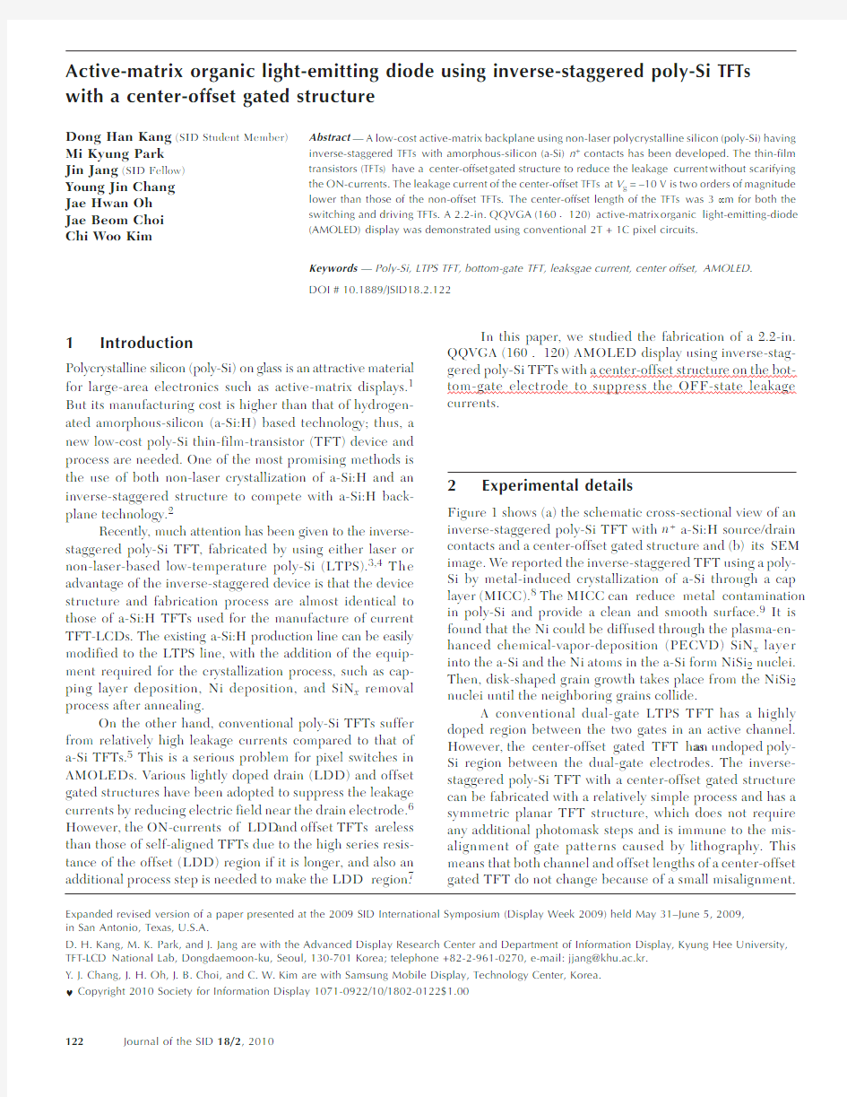
Figure1shows(a)the schematic cross-sectional view of an inverse-staggered poly-Si TFT with n+a-Si:H source/drain contacts and a center-offset gated structure and(b) its SEM image.We reported the inverse-staggered TFT using a poly-Si by metal-induced crystallization of a-Si through a cap layer(MICC).8The MICC can reduce metal contamination in poly-Si and provide a clean and smooth surface.9It is found that the Ni could be diffused through the plasma-en-hanced chemical-vapor-deposition(PECVD)SiN x layer into the a-Si and the Ni atoms in the a-Si form NiSi2nuclei. Then,disk-shaped grain growth takes place from the NiSi2 nuclei until the neighboring grains collide.
A conventional dual-gate LTPS TFT has a highly doped region between the two gates in an active channel. However,the center-offset gated TFT has an undoped poly-Si region between the dual-gate electrodes.The inverse-staggered poly-Si TFT with a center-offset gated structure can be fabricated with a relatively simple process and has a symmetric planar TFT structure,which does not require any additional photomask steps and is immune to the mis-alignment of gate patterns caused by lithography.This means that both channel and offset lengths of a center-offset gated TFT do not change because of a small misalignment.
Expanded revised version of a paper presented at the2009SID International Symposium(Display Week2009)held May31–June5,2009,
in San Antonio,Texas,U.S.A.
D.H.Kang,M.K.Park,and J.Jang are with the Advanced Display Research Center and Department of Information Display,Kyung Hee University, TFT-LCD National Lab,Dongdaemoon-ku,Seoul,130-701Korea;telephone+82-2-961-0270,e-mail:jjang@khu.ac.kr.
Y.J.Chang,J.H.Oh,J.B.Choi,and C.W.Kim are with Samsung Mobile Display,Technology Center,Korea.
?Copyright2010Society for Information Display1071-0922/10/1802-0122$1.00
122Journal of the SID18/2,2010
But the offset length can be changed in the drain-offset TFT by a small amount of misalignment.
MoW (100nm)was deposited on Corning 1737glass by DC sputtering for gate metal,and then the 100-nm SiO 2was deposited by PECVD at a RF power density of 0.1W/cm 2using a SiH 4/N 2O/He mixture at a substrate temperature of 340°C.An a-Si layer was deposited on the SiO 2(100nm)/MoW (100nm)/glass.
After its dehydrogenation,the 50-nm-thick SiN x was deposited by PECVD at a substrate temperature of 270°C,and then Ni particles were scattered onto the SiN x /a-Si by RF sputtering at high pressure.
The nickel density on the SiN x was 2×10¹⁴atoms/cm 2,which is less than a monolayer so that it is not a continuous layer.
Samples were heated at 580°C for
15hours in a fur-nace for crystallization.The SiN x cap layer on the poly-Si was etched away by a buffered oxide etch solution (NH 4F +HF +H 2O)after crystallization.Subsequently,we used n +a-Si:H for the source/drain contacts.Note that the ion-dop-ing process is conventionally adopted in the manufacturing of LTPS TFT arrays.The advantage of the TFT array with n +a-Si:H contacts and a poly-Si active layer is that the device structure and fabrication process are almost identical to those of a-Si TFTs.The active area of the TFT was defined
by NF 3plasma etching, and then a MoW layer for source/drain electrodes was deposited by DC sputtering.After patterning the MoW layer,the n +a-Si layer between the source and drain was etched away by using a dry process.The passivation layer of SiN x was deposited by PECVD and patterned to form via-holes by reactive ion etching (RIE).Device characterization and the application of OFF-state bias stress were performed using an Agilent 4156B device parameter analyzer.
3Results and discussion
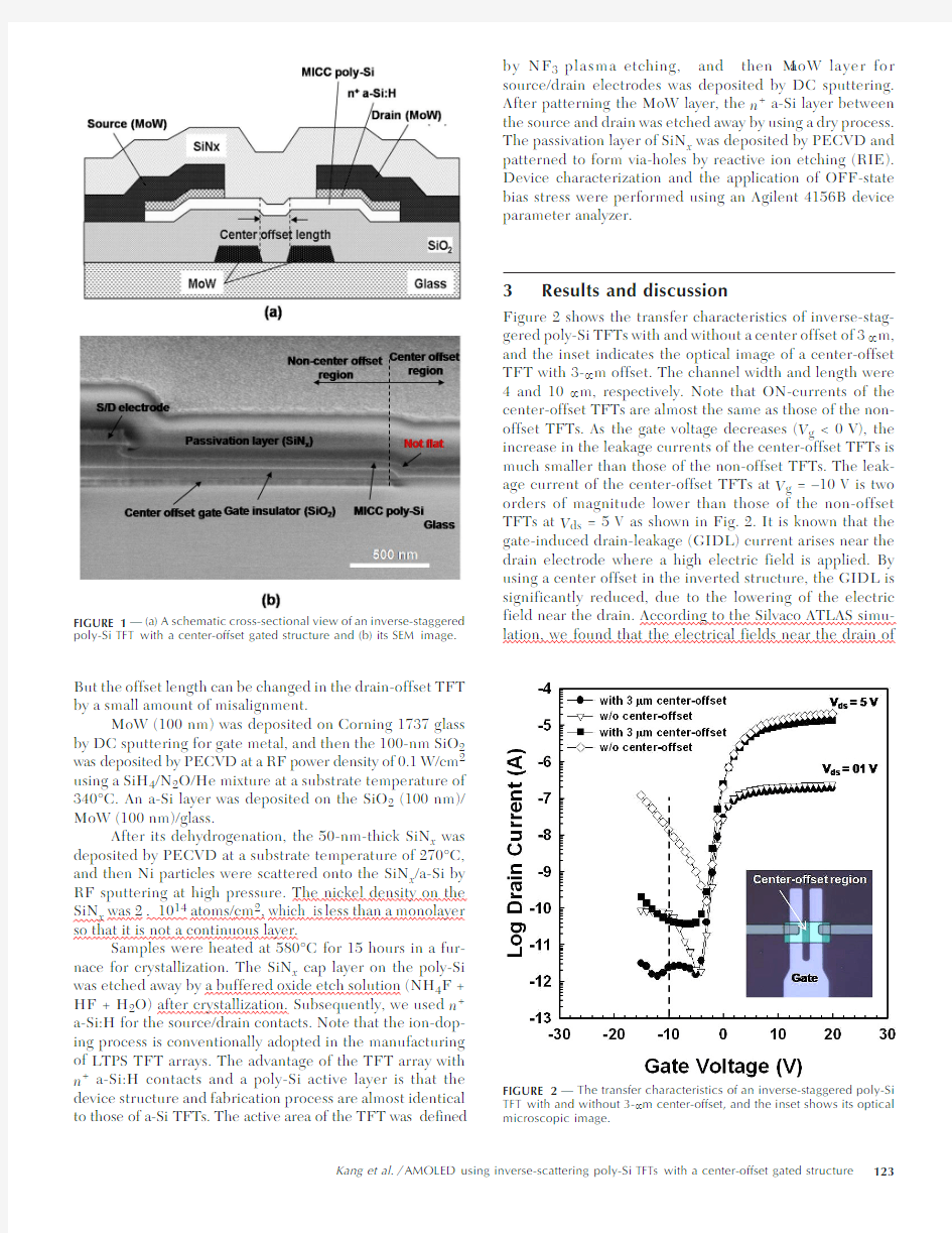
Figure 2shows the transfer characteristics of inverse-stag-gered poly-Si TFTs with and without a center offset of 3μm,and the inset indicates the optical image of a center-offset TFT with 3-μm offset.The channel width and length were 4and 10μm,respectively.Note that ON-currents of the center-offset TFTs are almost the same as those of the non-offset TFTs.As the gate voltage decreases (V g <0V),the increase in the leakage currents of the center-offset TFTs is much smaller than those of the non-offset TFTs.The leak-age current of the center-offset TFTs at V g =–10V is two orders of magnitude lower than those of the non-offset TFTs at V ds =5V as shown in Fig.2.It is known that the gate-induced drain-leakage (GIDL)current arises near the drain electrode where a high electric field is applied.By using a center offset in the inverted structure,the GIDL is significantly reduced,due to the lowering of the electric field near the drain.According to the Silvaco ATLAS simu-lation,we found that the electrical fields near the drain of
FIGURE 2—The transfer characteristics of an inverse-staggered poly-Si TFT with and without 3-μm center-offset,and the inset shows its optical microscopic image.
FIGURE 1—(a)A schematic cross-sectional view of an inverse-staggered poly-Si TFT with a center-offset gated structure and (b)its SEM image.
the center-offset TFT with an inverse-staggered structure decrease significantly compared with a non-offset TFT.Therefore,it is
concluded that the reduced drain field decreases OFF-state currents significantly without sacrificing on-cur-rent.10
It is found that the OFF-state currents are flat when varying the gate voltage by introducing the center-offset region in the channel of an inverse-staggered TFT,while a non-off-set TFT shows a sharp increase in drain current when decreasing the gate voltage.The ON-and OFF-currents are almost the same when varying the offset length between 2and 5μm,resulting in ON-and OFF-currents that are relatively insensitive to the offset length in the range of 2–5μm.10Therefore,it is concluded that the center-offset TFT exhibited its ON-state similar to a non-offset TFT and its OFF-state similar to an LDD TFT.11
Table 1shows the performance of the inverse-stag-gered poly-Si TFTs with and without a center-offset of 3-μm
length.The inverse-staggered poly-Si TFT without a center-offset exhibited a field-effect mobility of 23.8cm 2/V-sec.On the other hand,a center-offset gated TFT showed a field-effect mobility of 18.4cm 2/V-sec.This reduction in mobility is rather small compared with that of LDD TFTs.Note that the reduction of OFF-current is important for AMOLED application.12
Figure 3shows the threshold voltage and field-effect-mobility variation under a gate bias stress of +20V or –20V .The origin of the threshold voltage shift can be explained by charge trapping into SiO 2and deep-state creation in poly-Si.As shown in the figure,there is a slight shift in the thresh-old voltage after 10,000sec.And the field-effect mobility changes within +/–2%after a gate bias stress of +20V or –20V .These results show that a center-offset gated poly-Si TFT is highly stable under gate-bias stress either at positive or negative bias.Therefore,a center-offset gated TFT is suitable for the TFTs of AMOLEDs.
To demonstrate the feasibility of an inverse-staggered poly-Si TFT based AMOLED display,a small-sized mono-chrome display was fabricated.The display size was 2.2in.(diagonal)and its resolution was 160×120.Figure 4shows the CAD layout image of a 2.2-in.AMOLED panel.The gate line and data line were designed to be 8and 8μm,respectively,and the storage capacitor was 0.4pF to improve the VHR (voltage holding ratio).
FIGURE 3—Variation in threshold voltage and field-effect mobility for an inverse-staggered poly-Si TFT with a center-offset gated structure under a gate bias stress of (a)–20V and (b)+20V during 10,000sec.
TABLE 1—Comparison of the performances of the inverse-staggered poly-Si TFTs with and without a center-offset gated structure.The channel width and length are 4and 10μm,respectively.
FIGURE 4—The CAD layout image of a 2.2-in.AMOLED panel.
124Journal of the SID 18/2,2010
Figure 5 shows (a)the equivalent circuit of a pixel that is composed of two TFTs and one capacitor and (b)its opti-cal image of the pixels in an AMOLED backplane.All TFTs in the pixels were designed by a center-offset gated struc-ture and the W /L of the switching TFT and the driving TFT were 10/3+3and 90/3+3μm with 3μm of center-offset length,respectively.The pixel arrays were arranged by bilat-eral symmetry,called a mirror-type arrangement.Its advan-tage is having a wide pitch of the V DD line to reduce the resistance of power line and to decrease the probability of a short circuit between V DD and V data because of the space between the two pixels.
Figure 6shows (a)the chemical structures of organic materials and (b)the schematic energy diagrams of the green-phosphorescent OLEDs used in this work.The green-phosphorescent OLED was a conventional multi-layer structure.α-NPB,Alq 3and Balq were widely used as the hole-transporting layer,electron-transporting layer,and hole-blocking layer,respectively.For the high-efficiency green PHOLED,the emission layer was fabricated with 10%Ir(ppy)3doped in CBP host material.The device struc-
ture was IZO/α-NPB (40nm)/CBP:Ir(ppy)3(30nm)/Balq (5nm)/Alq 3(20nm)/LiF/Al.A conventional shadow-mask method was used for EL and cathode deposition.
Finally,we have fabricated a 2.2-in.AMOLED using an inverse-staggered poly-Si TFT backplane with a center-offset.The pixel size was 282×282μm and the aperture
FIGURE 5—(a)An equivalent circuit of the 2T +1C pixel and (b)its optical image.The pixel size is 282×282μm and the aperture ratio is about 53%.
FIGURE 6—(a)The chemical structures of organic materials and (b)the schematic energy diagrams of green-phosphorescent OLEDs.
FIGURE 7—The photograph of a 2.2-in.AMOLED using inverse-staggered poly-Si TFTs with a center-offset gated structure.
Kang et al./AMOLED using inverse-scattering poly-Si TFTs with a center-offset gated structure
125
ratio was about 53%.Two TFTs and one capacitor in a pixel were used to drive the OLED.
Figure 7 shows a photograph of an image displayed on the 2.2-in.AMOLED panel using inverse-staggered poly-Si TFTs with a center-offset.
Table 2summarizes the specifications for a bottom-emissive AMOLED with an aperture ratio of 53%.DC sig-nals were supplied on power lines (12V)and a common cathode electrode (0V),while pulsed voltages was continu-ously applied to all scan lines from –7to 18V .Despite some defect pixels (dark or bright spots),brightness variation can be clearly seen by V data signal modulation from 0to 7V .
4Conclusion
We have developed a 2.2-in.AMOLED display with center-offset inverse-staggered poly-Si TFTs.The device perform-ances such as field-effect mobility,gate voltage swing,V th ,and OFF-currents are almost independent on the offset length when it varies between 2and 5μm.In addition,the threshold voltage and field-effect mobility of the center-off-set gated TFT are stable under negative or positive gate bias stress.Therefore,the proposed TFT can be applied to the manufacture of a low-cost AMOLED backplane.Note that the OFF-state currents could be reduced by two orders of magnitude by using a center-offset device.
Acknowledgment
This research was supported by a grant (F0064062-2009-32)from the Information Display R&D Center,one of the Knowledge Economy Frontier R&D Programs funded by the Ministry of Knowledge Economy of Korean govern-ment.
References
1Y.M.Tsai et al.,“LTPS and AMOLED technologies for mobile dis-plays,”SID Symposium Digest 38,1451–1454(2007).
2T.Sasaoka et al.,“A 13.0-in. AMOLED display with top emitting structure and adaptive current mode programmed pixel circuit (TAC),”SID Symposium Digest 32,384–387(2001).
3K.S.Girotra et al.,“PECVD-based nanocrystalline-silicon TFT back-planes for large-sized AMOLED displays,”https://www.doczj.com/doc/c112120297.html,.Display 15,No.2,113–118(2007).
4M.Kunii,“Evaluation of electrical characteristics and trap-state den-sity in bottom-gate polycrystalline thin film transistors processed with high-pressure water vapor annealing,”Jpn.J.Appl.Phys.45,660–665(2006).
5J.G.Fossum et al.,“Anomalous leakage current in LPCVD poly-silicon MOSFET’s,”IEEE Trans.Electron Dev.32,1878–1884(1985).
6S.Seki et al.,“Laser-recrystallized polycrystalline-silicon thin-film transistors with low leakage current and high switching ratio,”IEEE Electron Dev.Lett.8,425–427(1987).
7 B.H.Min et al.,“A novel offset gated polysilicon thin film transistor without an additional offset mask,”IEEE Electron Dev. Lett.16,161–163(1995).
8J.H.Oh et al.,“Inverse staggered poly-Si thin-film transistor with non-laser crystallization of amorphous silicon,”Solid-State Electron.52,482–486(2008).
9J.H.Choi et al.,“Metal-induced lateral crystallization of amorphous silicon through a silicon nitride cap layer,”Electrochem.Solid-State Lett.6,G16(2003).
10J.H.Oh et al.,“A center-offset polycrystalline-silicon thin-film transis-tor with n +amorphous-silicon contacts,”IEEE Electron Dev.Lett.30,36–38(2009).
11N.Lifshitz et al.,“Active-gate thin-film transistor,”IEEE Electron Dev.
Lett.14,394–395(1993).
12Y.G.Lee et al.,“A comparison between a-Si:H TFT and poly-Si TFT
for a pixel in AMOLED,”J.Korean Phys.Soc.39,S291–S295(2001).
Dong Han Kang received his B.S.degree in mate-rial physics at Dong-A University,Busan,South Korea,in 2006,and his M.S.degree in physics at Kyung-Hee University,Seoul,South Korea,in 2008.He has been pursuing the Ph.D.degree at the Kyung-Hee University of Information Display,Seoul,South Korea.His current research is focused LTPS TFTs and AMOLED backplane using poly-Si TFTs.
Mi Kyung Park received her B.S.degree in mate-rial physics at Dong-A University,Busan,in 2008.She is currently a M.S course of Information Dis-play with Kyung Hee University,where she is un-der command of the Advanced Display Research Center.Her current research interests include polycrystalline-silicon thin-film transistor and AMOLED.
TABLE 2—The specification of a 2.2-in.AMOLED using inverse-staggered poly-Si TFTs with a center-offset gated
structure.
126
Journal of the SID 18/2,
2010
Jin Jang received his Ph.D.degree in physics from the Korean Advanced Institute of Science and Technology,Seoul, in 1982.He is currently a Pro-fessor of Information Display with Kyung Hee University,where he is in charge of the TFT-LCD National Laboratory and the Advanced Display Research Center.He has authored or co-authored over300technical publications in international journals.His current research interests include display devices,electronic devices using thin films,and organic electronics.
Young Jin Chang received his M.S.degrees from Kyung Hee University in Information Display.In Samsung Mobile Displays Co.,Ltd.,he is in charge of developing laser crystallization technol-ogy for low-temperature polycrystalline silicon TFT backplanes for AMOLED for both high-resolu-tion mobile application and large-area TV applica-tion.
Jae Hwan Oh received his B.S.degree of material physics in Dong-A University,Busan,South Korea, in2002,and his M.S.and Ph.D.degrees in Infor-mation Display in Kyung-Hee University,Seoul, South Korea,in2004and2009.In Samsung Mobile Displays Co.,Ltd.,he is in charge of developing laser crystallization technology for low-tempera-ture polycrystalline silicon TFT backplanes for AMOLED for both high-resolution mobile appli-cation and large-area TV application.Jae Beom Choi received his B.S.and M.S.degrees from Korea Advanced Institute of Science and Technology in materials science in1992and 1994,and his M.Phil.and Ph.D.degrees from Columbia University in applied physics and applied mathematics in2005and2006.At Samsung Mobile Displays Co.,Ltd.,he is in charge of developing laser crystallization technology for low-temperature polycrystalline silicon TFT back-planes for AMOLED for both high-resolution mobile application and large-area TV application.
Chi Woo Kim received his Ph.D.degree from the University of Texas at Austin in experimental con-densed matter physics in1989.He joined x-ray imaging group in University of Michigan at Ann Arbor as post-doctoral research fellow.In1991, he moved to Samsung Electronics Co.,Ltd.As a vice-president and team leader of the mobile dis-play process development team,he is leading the development and production of both a-Si and LTPS TFT-LCDs for mobile application.Currently, he joins to Samsung Mobile
Display.
Kang et al./AMOLED using inverse-scattering poly-Si TFTs with a center-offset gated structure127