April 2012Doc ID 022138 Rev 41/67
UM1461User manual
STM3240G-EVAL evaluation board
Introduction
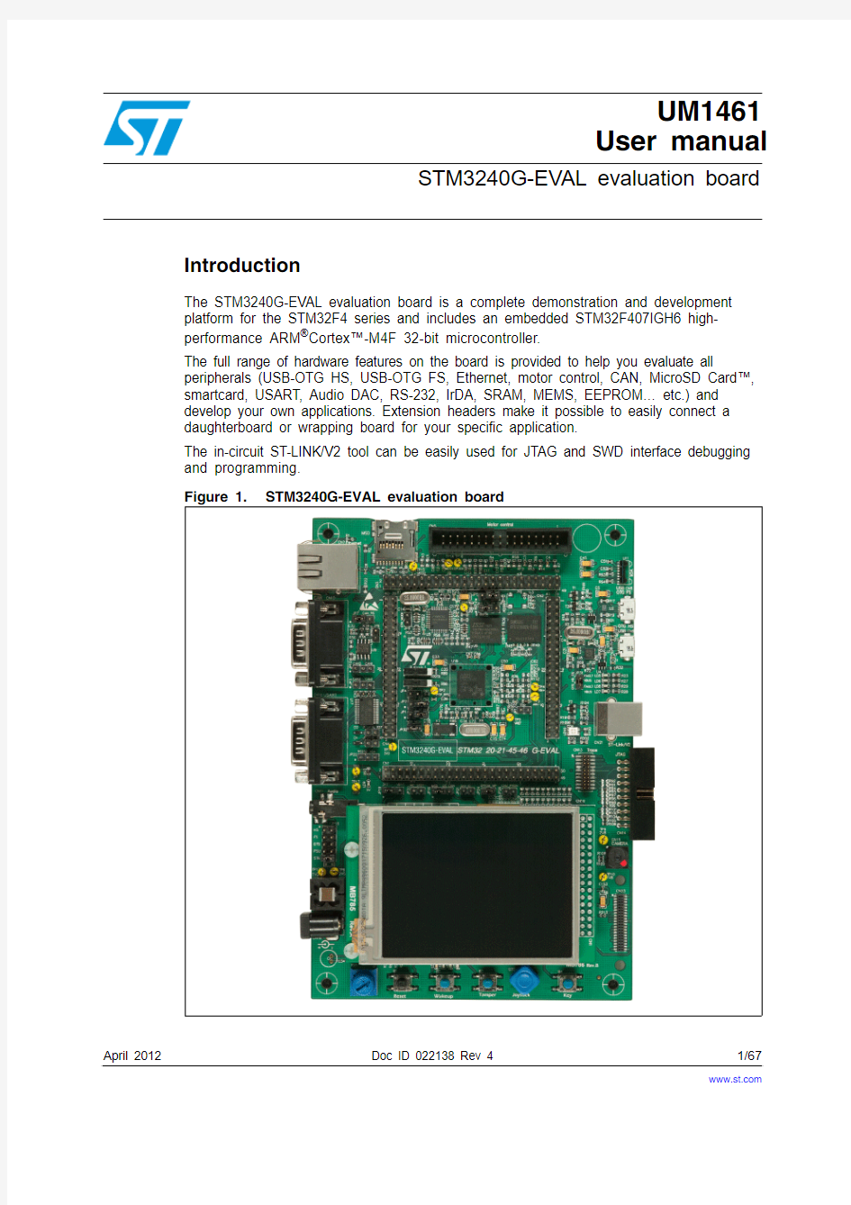
The STM3240G-EVAL evaluation board is a complete demonstration and development platform for the STM32F4 series and includes an embedded STM32F407IGH6 high-performance ARM ?Cortex?-M4F 32-bit microcontroller.
The full range of hardware features on the board is provided to help you evaluate all
peripherals (USB-OTG HS, USB-OTG FS, Ethernet, motor control, CAN, MicroSD Card?, smartcard, USART, Audio DAC, RS-232, IrDA, SRAM, MEMS, EEPROM… etc.) and develop your own applications. Extension headers make it possible to easily connect a daughterboard or wrapping board for your specific application.
The in-circuit ST-LINK/V2 tool can be easily used for JTAG and SWD interface debugging and programming.
Figure 1.
STM3240G-EVAL evaluation board
https://www.doczj.com/doc/c311470808.html,
Contents UM1461
Contents
1Overview . . . . . . . . . . . . . . . . . . . . . . . . . . . . . . . . . . . . . . . . . . . . . . . . . . 6
1.1Features . . . . . . . . . . . . . . . . . . . . . . . . . . . . . . . . . . . . . . . . . . . . . . . . . . . 6
1.2Demonstration software . . . . . . . . . . . . . . . . . . . . . . . . . . . . . . . . . . . . . . . 6
1.3Order code . . . . . . . . . . . . . . . . . . . . . . . . . . . . . . . . . . . . . . . . . . . . . . . . . 6
1.4Delivery recommendations . . . . . . . . . . . . . . . . . . . . . . . . . . . . . . . . . . . . . 7
2Hardware layout and configuration . . . . . . . . . . . . . . . . . . . . . . . . . . . . . 8
2.1Power supply . . . . . . . . . . . . . . . . . . . . . . . . . . . . . . . . . . . . . . . . . . . . . . 11
2.2Boot option . . . . . . . . . . . . . . . . . . . . . . . . . . . . . . . . . . . . . . . . . . . . . . . . 12
2.3Clock source . . . . . . . . . . . . . . . . . . . . . . . . . . . . . . . . . . . . . . . . . . . . . . . 13
2.4Reset source . . . . . . . . . . . . . . . . . . . . . . . . . . . . . . . . . . . . . . . . . . . . . . 13
2.5Audio . . . . . . . . . . . . . . . . . . . . . . . . . . . . . . . . . . . . . . . . . . . . . . . . . . . . 13
2.6EEPROM . . . . . . . . . . . . . . . . . . . . . . . . . . . . . . . . . . . . . . . . . . . . . . . . . 14
2.7CAN . . . . . . . . . . . . . . . . . . . . . . . . . . . . . . . . . . . . . . . . . . . . . . . . . . . . . 14
2.8RS-232 and IrDA . . . . . . . . . . . . . . . . . . . . . . . . . . . . . . . . . . . . . . . . . . . 15
2.9Motor control . . . . . . . . . . . . . . . . . . . . . . . . . . . . . . . . . . . . . . . . . . . . . . 16
2.10Smartcard . . . . . . . . . . . . . . . . . . . . . . . . . . . . . . . . . . . . . . . . . . . . . . . . . 17
2.11MicroSD Card . . . . . . . . . . . . . . . . . . . . . . . . . . . . . . . . . . . . . . . . . . . . . . 17
2.12MEMS . . . . . . . . . . . . . . . . . . . . . . . . . . . . . . . . . . . . . . . . . . . . . . . . . . . . 18
2.13Potentiometer . . . . . . . . . . . . . . . . . . . . . . . . . . . . . . . . . . . . . . . . . . . . . . 18
2.14ADC . . . . . . . . . . . . . . . . . . . . . . . . . . . . . . . . . . . . . . . . . . . . . . . . . . . . . 18
2.15USB-OTG FS . . . . . . . . . . . . . . . . . . . . . . . . . . . . . . . . . . . . . . . . . . . . . . 18
2.16Ethernet . . . . . . . . . . . . . . . . . . . . . . . . . . . . . . . . . . . . . . . . . . . . . . . . . . 18
2.17USB-OTG HS . . . . . . . . . . . . . . . . . . . . . . . . . . . . . . . . . . . . . . . . . . . . . . 19
2.18Camera module . . . . . . . . . . . . . . . . . . . . . . . . . . . . . . . . . . . . . . . . . . . . 20
2.19SRAM . . . . . . . . . . . . . . . . . . . . . . . . . . . . . . . . . . . . . . . . . . . . . . . . . . . . 21
2.20Development and debug support . . . . . . . . . . . . . . . . . . . . . . . . . . . . . . . 21
2.21Display and input devices . . . . . . . . . . . . . . . . . . . . . . . . . . . . . . . . . . . . . 23
3Connectors . . . . . . . . . . . . . . . . . . . . . . . . . . . . . . . . . . . . . . . . . . . . . . . 24
3.1Daughterboard extension connectors CN1, 2, 3 and 4 . . . . . . . . . . . . . . 24 2/67Doc ID 022138 Rev 4
UM1461Contents
3.2Motor control connector CN5 . . . . . . . . . . . . . . . . . . . . . . . . . . . . . . . . . . 31
3.3MicroSD connector CN6 . . . . . . . . . . . . . . . . . . . . . . . . . . . . . . . . . . . . . . 32
3.4Ethernet RJ45 connector CN7 . . . . . . . . . . . . . . . . . . . . . . . . . . . . . . . . . 32
3.5USB-OTG FS Micro-AB connector CN8 . . . . . . . . . . . . . . . . . . . . . . . . . . 33
3.6USB-OTG HS Micro-AB connector CN9 . . . . . . . . . . . . . . . . . . . . . . . . . 33
3.7CAN D-type 9-pin male connectors CN10 (CAN1 or CAN2) . . . . . . . . . . 34
3.8Audio connector CN11 . . . . . . . . . . . . . . . . . . . . . . . . . . . . . . . . . . . . . . . 34
3.9T race debugging connector CN13 . . . . . . . . . . . . . . . . . . . . . . . . . . . . . . 34
3.10JTAG debugging connector CN14 . . . . . . . . . . . . . . . . . . . . . . . . . . . . . . 35
3.11Camera module connector CN15 . . . . . . . . . . . . . . . . . . . . . . . . . . . . . . . 35
3.12RS-232 connector CN16 . . . . . . . . . . . . . . . . . . . . . . . . . . . . . . . . . . . . . 36
3.13Power connector CN18 . . . . . . . . . . . . . . . . . . . . . . . . . . . . . . . . . . . . . . 36
3.14TFT LCD connector CN19 . . . . . . . . . . . . . . . . . . . . . . . . . . . . . . . . . . . . 37
3.15Smartcard connector CN20 . . . . . . . . . . . . . . . . . . . . . . . . . . . . . . . . . . . 37
3.16ST-LINK/V2 connector CN21 . . . . . . . . . . . . . . . . . . . . . . . . . . . . . . . . . . 37
3.17Camera extension connector CN23 . . . . . . . . . . . . . . . . . . . . . . . . . . . . . 38
3.18STM3240G-EVAL pinout . . . . . . . . . . . . . . . . . . . . . . . . . . . . . . . . . . . . . 38 4Schematics . . . . . . . . . . . . . . . . . . . . . . . . . . . . . . . . . . . . . . . . . . . . . . . 44 5Revision history . . . . . . . . . . . . . . . . . . . . . . . . . . . . . . . . . . . . . . . . . . . 66
Doc ID 022138 Rev 43/67
List of tables UM1461 List of tables
Table 1.Power related jumpers and solder bridges. . . . . . . . . . . . . . . . . . . . . . . . . . . . . . . . . . . . . 11 Table 2.Boot related jumpers. . . . . . . . . . . . . . . . . . . . . . . . . . . . . . . . . . . . . . . . . . . . . . . . . . . . . . 12 Table 3.Audio related jumpers. . . . . . . . . . . . . . . . . . . . . . . . . . . . . . . . . . . . . . . . . . . . . . . . . . . . . 13 Table 4.EEPROM related jumper and solder bridge. . . . . . . . . . . . . . . . . . . . . . . . . . . . . . . . . . . . 14 Table 5.CAN-related jumpers . . . . . . . . . . . . . . . . . . . . . . . . . . . . . . . . . . . . . . . . . . . . . . . . . . . . . 14 Table 6.RS-232 and IrDA related jumper . . . . . . . . . . . . . . . . . . . . . . . . . . . . . . . . . . . . . . . . . . . . 15 Table 7.Motor control solder bridges. . . . . . . . . . . . . . . . . . . . . . . . . . . . . . . . . . . . . . . . . . . . . . . . 16 Table 8.Connection between ST8024 and STM32F407IGH6. . . . . . . . . . . . . . . . . . . . . . . . . . . . . 17 Table 9.Smartcard related jumper. . . . . . . . . . . . . . . . . . . . . . . . . . . . . . . . . . . . . . . . . . . . . . . . . . 17 Table 10.MicroSD Card related jumpers. . . . . . . . . . . . . . . . . . . . . . . . . . . . . . . . . . . . . . . . . . . . . . 17 Table 11.Ethernet related jumpers and solder bridges . . . . . . . . . . . . . . . . . . . . . . . . . . . . . . . . . . . 18 Table 12.MicroSD Card related jumper. . . . . . . . . . . . . . . . . . . . . . . . . . . . . . . . . . . . . . . . . . . . . . . 19 Table 13.Camera module related jumpers . . . . . . . . . . . . . . . . . . . . . . . . . . . . . . . . . . . . . . . . . . . . 20 Table 14.SRAM related jumpers . . . . . . . . . . . . . . . . . . . . . . . . . . . . . . . . . . . . . . . . . . . . . . . . . . . . 21 Table 15.Third-party toolchain support . . . . . . . . . . . . . . . . . . . . . . . . . . . . . . . . . . . . . . . . . . . . . . . 21 Table 16.LCD modules . . . . . . . . . . . . . . . . . . . . . . . . . . . . . . . . . . . . . . . . . . . . . . . . . . . . . . . . . . . 23 Table 17.Daughterboard extension connector CN1 . . . . . . . . . . . . . . . . . . . . . . . . . . . . . . . . . . . . . 24 Table 18.Daughterboard extension connector CN2 . . . . . . . . . . . . . . . . . . . . . . . . . . . . . . . . . . . . . 26 Table 19.Daughterboard extension connector CN3 . . . . . . . . . . . . . . . . . . . . . . . . . . . . . . . . . . . . . 27 Table 20.Daughterboard extension connector CN4 . . . . . . . . . . . . . . . . . . . . . . . . . . . . . . . . . . . . . 29 Table 21.Motor control connector CN5 . . . . . . . . . . . . . . . . . . . . . . . . . . . . . . . . . . . . . . . . . . . . . . . 31 Table 22.MicroSD connector CN6. . . . . . . . . . . . . . . . . . . . . . . . . . . . . . . . . . . . . . . . . . . . . . . . . . . 32 Table 23.RJ45 connector CN7 . . . . . . . . . . . . . . . . . . . . . . . . . . . . . . . . . . . . . . . . . . . . . . . . . . . . . 32 Table https://www.doczj.com/doc/c311470808.html,B-OTG FS Micro-AB connector CN8. . . . . . . . . . . . . . . . . . . . . . . . . . . . . . . . . . . . . . . 33 Table https://www.doczj.com/doc/c311470808.html,B-OTG HS Micro-AB connector CN9. . . . . . . . . . . . . . . . . . . . . . . . . . . . . . . . . . . . . . . 33 Table 26.CAN D-type 9-pin male connector CN10 (CAN1 or CAN2) . . . . . . . . . . . . . . . . . . . . . . . . 34 Table 27.Trace debugging connector CN13 . . . . . . . . . . . . . . . . . . . . . . . . . . . . . . . . . . . . . . . . . . . 34 Table 28.JTAG debugging connector CN14 . . . . . . . . . . . . . . . . . . . . . . . . . . . . . . . . . . . . . . . . . . . 35 Table 29.Camera module connector CN15. . . . . . . . . . . . . . . . . . . . . . . . . . . . . . . . . . . . . . . . . . . . 35 Table 30.RS-232 connector CN16 with ISP support. . . . . . . . . . . . . . . . . . . . . . . . . . . . . . . . . . . . . 36 Table 31.Smartcard connector CN20 . . . . . . . . . . . . . . . . . . . . . . . . . . . . . . . . . . . . . . . . . . . . . . . . 37 Table 32.Camera extension connector CN23 . . . . . . . . . . . . . . . . . . . . . . . . . . . . . . . . . . . . . . . . . . 38 Table 33.STM3240G-EVAL pinout . . . . . . . . . . . . . . . . . . . . . . . . . . . . . . . . . . . . . . . . . . . . . . . . . . 38 Table 34.Document revision history . . . . . . . . . . . . . . . . . . . . . . . . . . . . . . . . . . . . . . . . . . . . . . . . . 66 4/67Doc ID 022138 Rev 4
UM1461List of figures List of figures
Figure 1.STM3240G-EVAL evaluation board. . . . . . . . . . . . . . . . . . . . . . . . . . . . . . . . . . . . . . . . . . . 1 Figure 2.Hardware layout and configuration. . . . . . . . . . . . . . . . . . . . . . . . . . . . . . . . . . . . . . . . . . . . 9 Figure 3.STM3240G-EVAL evaluation board layout. . . . . . . . . . . . . . . . . . . . . . . . . . . . . . . . . . . . . 10 Figure 4.Hardware layout and configuration. . . . . . . . . . . . . . . . . . . . . . . . . . . . . . . . . . . . . . . . . . . 10 Figure 5.STM3240G-EVAL evaluation board layout. . . . . . . . . . . . . . . . . . . . . . . . . . . . . . . . . . . . . 10 Figure 6.Pin 1 camera plug. . . . . . . . . . . . . . . . . . . . . . . . . . . . . . . . . . . . . . . . . . . . . . . . . . . . . . . . 20 Figure 7.Motor control connector CN5 . . . . . . . . . . . . . . . . . . . . . . . . . . . . . . . . . . . . . . . . . . . . . . . 31 Figure 8.MicroSD connector CN6. . . . . . . . . . . . . . . . . . . . . . . . . . . . . . . . . . . . . . . . . . . . . . . . . . . 32 Figure 9.Ethernet RJ45 connector CN7 . . . . . . . . . . . . . . . . . . . . . . . . . . . . . . . . . . . . . . . . . . . . . . 32 Figure https://www.doczj.com/doc/c311470808.html,B-OTG FS Micro-AB connector CN8. . . . . . . . . . . . . . . . . . . . . . . . . . . . . . . . . . . . . . . 33 Figure https://www.doczj.com/doc/c311470808.html,B-OTG HS Micro-AB connector CN9 . . . . . . . . . . . . . . . . . . . . . . . . . . . . . . . . . . . . . . 33 Figure 12.CAN D-type 9-pin male connector CN10 (CAN1 or CAN2) . . . . . . . . . . . . . . . . . . . . . . . . 34 Figure 13.Trace debugging connector CN13 . . . . . . . . . . . . . . . . . . . . . . . . . . . . . . . . . . . . . . . . . . . 34 Figure 14.JTAG debugging connector CN14 . . . . . . . . . . . . . . . . . . . . . . . . . . . . . . . . . . . . . . . . . . . 35 Figure 15.Camera module connector CN15 (front view). . . . . . . . . . . . . . . . . . . . . . . . . . . . . . . . . . . 35 Figure 16.RS-232 connector CN16 with ISP support (front view). . . . . . . . . . . . . . . . . . . . . . . . . . . . 36 Figure 17.Power supply connector CN18. . . . . . . . . . . . . . . . . . . . . . . . . . . . . . . . . . . . . . . . . . . . . . 36 Figure 18.Smartcard connector CN20 . . . . . . . . . . . . . . . . . . . . . . . . . . . . . . . . . . . . . . . . . . . . . . . . 37 Figure 19.STM3240G-EVAL. . . . . . . . . . . . . . . . . . . . . . . . . . . . . . . . . . . . . . . . . . . . . . . . . . . . . . . . 45 Figure 20.MCU . . . . . . . . . . . . . . . . . . . . . . . . . . . . . . . . . . . . . . . . . . . . . . . . . . . . . . . . . . . . . . . . . . 46 Figure https://www.doczj.com/doc/c311470808.html,B-OTG HS. . . . . . . . . . . . . . . . . . . . . . . . . . . . . . . . . . . . . . . . . . . . . . . . . . . . . . . . . . . 47 Figure 22.Camera. . . . . . . . . . . . . . . . . . . . . . . . . . . . . . . . . . . . . . . . . . . . . . . . . . . . . . . . . . . . . . . . 48 Figure 23.Ethernet . . . . . . . . . . . . . . . . . . . . . . . . . . . . . . . . . . . . . . . . . . . . . . . . . . . . . . . . . . . . . . . 49 Figure 24.Audio . . . . . . . . . . . . . . . . . . . . . . . . . . . . . . . . . . . . . . . . . . . . . . . . . . . . . . . . . . . . . . . . . 50 Figure https://www.doczj.com/doc/c311470808.html,B-OTG FS . . . . . . . . . . . . . . . . . . . . . . . . . . . . . . . . . . . . . . . . . . . . . . . . . . . . . . . . . . . 51 Figure 26.SRAM . . . . . . . . . . . . . . . . . . . . . . . . . . . . . . . . . . . . . . . . . . . . . . . . . . . . . . . . . . . . . . . . 52 Figure 27.LCD . . . . . . . . . . . . . . . . . . . . . . . . . . . . . . . . . . . . . . . . . . . . . . . . . . . . . . . . . . . . . . . . . . 53 Figure 28.RS-232 and IrDA . . . . . . . . . . . . . . . . . . . . . . . . . . . . . . . . . . . . . . . . . . . . . . . . . . . . . . . . 54 Figure 29.CAN . . . . . . . . . . . . . . . . . . . . . . . . . . . . . . . . . . . . . . . . . . . . . . . . . . . . . . . . . . . . . . . . . . 55 Figure 30.I/O peripherals . . . . . . . . . . . . . . . . . . . . . . . . . . . . . . . . . . . . . . . . . . . . . . . . . . . . . . . . . . 56 Figure 31.I/O expandor. . . . . . . . . . . . . . . . . . . . . . . . . . . . . . . . . . . . . . . . . . . . . . . . . . . . . . . . . . . . 57 Figure 32.MicroSD Card. . . . . . . . . . . . . . . . . . . . . . . . . . . . . . . . . . . . . . . . . . . . . . . . . . . . . . . . . . . 58 Figure 33.Motor control . . . . . . . . . . . . . . . . . . . . . . . . . . . . . . . . . . . . . . . . . . . . . . . . . . . . . . . . . . . 59 Figure 34.Smartcard. . . . . . . . . . . . . . . . . . . . . . . . . . . . . . . . . . . . . . . . . . . . . . . . . . . . . . . . . . . . . . 60 Figure 35.JTAG and Trace. . . . . . . . . . . . . . . . . . . . . . . . . . . . . . . . . . . . . . . . . . . . . . . . . . . . . . . . . 61 Figure 36.Power . . . . . . . . . . . . . . . . . . . . . . . . . . . . . . . . . . . . . . . . . . . . . . . . . . . . . . . . . . . . . . . . . 62 Figure 37.Extension connector. . . . . . . . . . . . . . . . . . . . . . . . . . . . . . . . . . . . . . . . . . . . . . . . . . . . . . 63 Figure 38.STLINK/V2 . . . . . . . . . . . . . . . . . . . . . . . . . . . . . . . . . . . . . . . . . . . . . . . . . . . . . . . . . . . . . 64 Figure 39. 3.2” LCD module with SPI and 16-bit interface. . . . . . . . . . . . . . . . . . . . . . . . . . . . . . . . . . 65
Doc ID 022138 Rev 45/67
Overview UM1461
6/67Doc ID 022138 Rev 4
1 Overview
1.1 Features
●STM32F407IGH6 microcontroller.●16 Mbit SRAM
● 1 Gbyte or more MicroSD Card
●Boot from user Flash, system memory or SRAM ●Both ISO/IEC 14443 type A and B smartcard support
●I 2C compatible serial interface 8 Kbytes EEPROM, MEMS and I/O expander ●IEEE 802.3-2002 compliant Ethernet connector ●Two CAN 2.0 A/B channels on the same DB connector ●RS-232 communication ●IrDA transceiver
●USB-OTG (HS and FS) with Micro-AB connector ●Inductor motor control connector
●I 2S Audio DAC, stereo audio jack for headset ● 3.2" 240x320 TFT color LCD with touchscreen ● 4 color LEDs
●Camera module and extension connector for ST camera plug-in ●Joystick with 4-direction control and selector ●Reset, wakeup, tamper and user button ●RTC with backup battery
●Extension connector for daughterboard or wrapping board ●JTAG, SWD and trace debug support ●Embedded ST -LINK/V2
●
Five 5 V power supply options: Power jack, USB FS connector, USB HS connector, ST -LINK/V2 or daughterboard
1.2 Demonstration software
Demonstration software is preloaded in the board's Flash memory for easy demonstration of
the device peripherals in standalone mode. For more information and to download the latest version, please refer to STM3240G-EVAL demonstration software available on web: https://www.doczj.com/doc/c311470808.html,/mcu
1.3 Order code
To order the STM32F407IGH6 MCU evaluation board, use order code STM3240G-EVAL.
UM1461Overview
Doc ID 022138 Rev 47/67
1.4 Delivery recommendations
Several verifications are needed before using the board for the first time to make sure that
nothing has been damaged during shipment and no components are unplugged and lost. When the board is extracted from its plastic bag, please check that no component remains in the bag. Main components to verify are:1.The 25 MHz crystals (X1 and X4) may have been removed by a shock.
2.
The camera connected on socket CN15 located on the right side of the board under the JTAG connector may be unplugged. If this is the case, please refer to the note in Section 2.18: Camera module to make sure to plug it in the correct position. 3.
The MicroSD Card may have been ejected from its connector CN6 (top left corner of the board).
The plastic protection on the camera should be removed carefully as the connection is very fragile.
2 Hardware layout and configuration
The STM3240G-EVAL evaluation board is designed around the STM32F407IGH6 in the
UFBGA176 package. The hardware block diagram Figure 4 illustrates the connection
between the STM32F407IGH6 and the peripherals (camera module, LCD, SRAM,
EEPROM, MEMS, USART, IrDA, USB-OTG HS, USB OTG FS, Ethernet, Audio, CAN bus,
smartcard, MicroSD Card and motor control) and Figure 5 will help you locate these
features on the actual evaluation board.
8/67Doc ID 022138 Rev 4
Doc ID 022138 Rev 49/67
10/67Doc ID 022138 Rev 4
2.1 Power
supply
The STM3240G-EVAL evaluation board is designed to be powered by 5 V DC power supply
and to be protected by PolyZen from a wrong power plug-in event. It is possible to configure
the evaluation board to use any of following five sources for the power supply:
● 5 V DC power adapter connected to CN18, the power jack on the board
● 5 V DC power with 500 mA limitation from CN8, the USB-OTG FS Micro-AB connector
● 5 V DC power with 500 mA limitation from CN9, the USB-OTG HS Micro-AB connector
● 5 V DC power with 500 mA limitation from CN21, the ST-LINK/V2 USB connector
● 5 V DC power from both CN1 and CN3, the extension connector for daughterboard
(DTB for daughterboard on silkscreen)
The power supply is configured by setting the related jumpers JP4, JP32, JP18 and JP19 as
described in T able 1.
Table 1.Power related jumpers and solder bridges
Jumper Description
JP4JP4 should be fitted to enable power down reset (PDR). PDR is disabled when JP4 is not fitted.
Default setting: Fitted.
JP32MCU_VDD is connected to 3.3V power when JP32 is closed and MCU current consumption measurement can be done manually by multi-meter when JP32 is open.
Default setting: Fitted.
JP18JP18 is used to select one of the five possible power supply sources.
T o select the ST-LINK/V2 USB connector (CN21) power
supply, set JP18 as shown:
(Default setting)
T o select power supply jack (CN18) power supply, set
JP18 as shown:
T o select daughterboard connector (CN1 and CN3)power
supply, set JP18 as shown:
HS
FS
DTB
PSU
STlk
HS
FS
DTB
PSU
STlk
HS
FS
DTB
PSU
STlk
Doc ID 022138 Rev 411/67
12/67Doc ID 022138 Rev 4
Note:
The LED LD9 is lit when the STM3240G-EVAL evaluation board is powered by the 5V correctly.
2.2 Boot option
The STM3240G-EVAL evaluation board is able to boot from:
●Embedded user Flash
●System memory with boot loader for ISP ●
Embedded SRAM for debugging
The boot option is configured by setting switches SW1 (BOOT1) and SW2 (BOOT0).
BOOT0 can also be configured via RS-232 connector CN16.
JP18(cont.)
T o select USB-OTG FS (CN8) power supply, set JP18 as shown:
T o select USB-OTG HS (CN9)power supply, set JP18 as shown:
T o select power supply jack (CN18) power supply to both STM3240G-EVAL and daughterboard connected on CN1 and CN3, set JP18 as shown (daughterboard must not have its own power supply connected )
JP19
T o connect Vbat to the battery, set JP19 as shown:
T o connect Vbat to 3.3V power, set JP19 as shown: (Default setting)
Table 1.
Power related jumpers and solder bridges (continued)
Jumper
Description
HS FS DTB PSU STlk
HS FS DTB PSU STlk
HS FS DTB PSU STlk
3
213
21Table 2.
Boot related jumpers
BOOT 0
BOOT 1Boot source
0Don’t care
STM3240G-EVAL boots from User Flash (Default setting)11STM3240G-EVAL boots from Embedded SRAM 1
STM3240G-EVAL boots from System Memory
2.3 Clock
source
Four clock sources are available on the STM3240G-EVAL evaluation board for
STM32F407IGH6 and RTC embedded:
●X1, 25 MHz crystal for Ethernet PHY with socket. It can be removed when clock is
provided by the MCU MCO pin
●X2, 26 MHz crystal for USB-OTG HS PHY
●X3, 32 kHz crystal for embedded RTC
●X4, 25 MHz crystal with socket for the,STM32F407IGH6 microcontroller (it can be
removed from socket when internal RC clock is used)
2.4 Reset
source
The reset signal of the STM3240G-EVAL evaluation board is low active and the reset
sources include:
●Reset button B1
●Debugging tools from JTAG connector CN14 and trace connector CN13
●Daughterboard from CN3
●RS-232 connector CN916 for ISP
●ST-LINK/V2
2.5 Audio
The STM3240G-EVAL evaluation board enables stereo audio play and microphone
recording by an external headset connected on audio jack CN11. An audio DAC CS43L22 is
connected to both I2S2 port and a DAC channel and a microphone amplifier is connected to
the ADC of the STM32F407IGH6. CS43L22 can be configured via I2C1 and the external
PLL (U36) can be used to provide external clock which is connected to I2S_CKIN pin (PC9). Note:To avoid speaker damage it is mandatory to connect the headphone to the board on CN11 during debug of audio code. When the program is stopped on a breakpoint, a DC voltage
may be applied to the speaker which induces power consumption incompatible with the
speaker.
Warning:Signal I2S_SD (PI3) is close to signal TCK/SWCLK of the
JTAG/SWD interface, so to avoid possible communication
issues on JTAG/SWD when the I2S interface is used the
recommendations are to:
1) Prefer usage of embedded ST-LINK/V2 to external tool
connected on CN14.
2) Configure PI3 GPIO in low speed (2 MHz or 10 MHz).
Table 3.Audio related jumpers
Jumper Description
JP16Description of JP16 is in Table 10 on page 17.
JP33The microphone amplifier can be disabled when JP33 is fitted.Default setting: Not fitted
Doc ID 022138 Rev 413/67
14/67Doc ID 022138 Rev 4
2.6 EEPROM
A 64 Kbit EEPROM is connected to the I2C1 bus of the STM32F407IGH6.
2.7 CAN
The STM3240G-EVAL evaluation board enables two channels of CAN2.0A/B compliant CAN bus communication based on a 3.3V CAN transceiver on one DB9 connector (CN10). The two CAN buses can be disconnected by jumpers from relevant STM32F407IGH6 I/Os which are shared with FSMC and USB-OTG HS. Jumpers JP3 and JP10 must be refit to enable CAN1 or CAN2 as listed in Table 5.
High-speed, Standby and Slope Control modes are available and can be selected by setting jumper JP7.
Table 4.EEPROM related jumper and solder bridge
Jumper Description
JP24
The EEPROM is in Write Protection mode when JP24 is not fitted.Default Setting: Not fitted
Table 5.CAN-related jumpers
Jumper
Description
JP3
To connect CAN1_TX to CAN transceiver, set JP3 as shown:
To connect CAN2_TX to CAN transceiver, set JP3 as shown:
JP10
To connect CAN1_RX to CAN transceiver, set JP10 as shown:
To connect CAN2_RX to CAN transceiver, set JP10 as shown:
PD0 and PB5 are disconnected from the CAN transceiver and used for FSMC and USB_OTG_HS when jumper JP10 is not fitted (default setting).JP7
To enable the selected CAN transceiver to work in Standby mode, set JP7 as shown:
To enable the selected CAN transceiver to work in High-speed mode, set JP7 as shown (default setting):
To enable the selected CAN transceiver to work in Slope Control mode, do not fit a jumper on JP7.
JP9
To enable the terminal resistor for the selected CAN, fit a jumper on JP9.(Default setting: not fitted)
3
213
213
213
213213
21
2.8 RS-232
and
IrDA
Both RS-232 and IrDA communication is enabled by D-type, 9-pin RS-232 connectors
(CN16) and IrDA transceiver U11 which are connected to USART3 of STM32F407IGH6 on
the STM3240G-EVAL evaluation board.
For ISP support, two signals are added on the RS-232 connector CN16:
●Bootloader_RESET (shared with CTS signal)
●Bootloader_BOOT0 (shared with DSR signal)
RS-232 or IrDA can be selected via JP22, ISP can be enabled via JP29 and JP34.
Table 6.RS-232 and IrDA related jumper
Jumper Description
JP22T o connect USART3_RX to IrDA transceiver and enable IrDA communication, set JP22 as shown:
T o connect USART3_RX to RS-232 transceiver and enable RS-232 communication, set JP22 as shown (Default setting):
T o enable MicroSD Card, which shares same I/Os with RS-232, JP22 is not fitted.
JP29Bootloader_BOOT0 is managed by pin 6 of CN16 (RS-232 DSR signal) when JP29 is closed. This configuration is used for boot loader application only.
Default setting: Not fitted.
JP34Bootloader_RESET is managed by pin 8 of CN16 (RS-232 CTS signal) when JP34 is fitted. This configuration is used for boot loader application only.
Default setting: Not fitted.
3
2
1
3
2
1
Doc ID 022138 Rev 415/67
16/67Doc ID 022138 Rev 4
2.9 Motor control
The STM3240G-EVAL evaluation board enables a three-phase brushless motor control via
a 34- pin connector (CN5), which provides all required control and feedback signals to and from the motor power-driving board. Available signals on this connector include emergency stop, motor speed, 3-phase motor current, bus voltage, heatsink temperature coming from the motor driving board and 6 channels of PWM control signal going to the motor driving circuit.
The solder bridge (SB18) allows to choose two kinds of synchronization methods for PFCs (Power Factor Correction) while the SB17 can be set for different signals on pin 31 of CN5.The I/O pins used on motor control connector CN5 are multiplexed with some peripherals on the board; either motor control connector or multiplexed peripherals can be enabled by the setting of solder bridges SB10, SB11, SB12, SB14, SB15 and SB16.
Note:1
Some 0 Ohm resistors have to be removed or soldered to enable motor control application except the solder bridges configurations mentioned above: – R34, R58 & R51 to be removed – R66, R204 & R205 to be soldered
2MicroSD Card must be removed from CN6 for motor control application.
Table 7.
Motor control solder bridges
Solder bridge
Description
Multiplexed peripherals
SB18
When closed, SB18 redirects the PFC synchronized signal to the timer 3 input capture pin 2 in addition to the timer 3 external trigger input.
Default setting: Open
SB17
For CN5 encoder signal input (pin 31), SB17 must be open.
For CN5 special motor analog signal input (pin 31), SB17 must be closed.
Default setting: Open
SB16
T o connect MC_EmergencySTOP to PI4, close SB16.Default setting: Open
Camera module connected to
CN15SB10T o connect MC_EnIndex to PB8, close SB10.Default setting: Open
Ethernet SB11T o connect MC_CurrentA to PC1, close SB11.Default setting: Open
SB12T o connect MC_CurrentB to PC2, close SB12.Default setting: Open
SB14T o connect MC_EnB to PD13, close SB14.Default setting: Open
FSMC
SB15
T o connect MC_EnA to PD12 close SB15.Default setting: Open
Doc ID 022138 Rev 417/67
2.10 Smartcard
STMicroelectronics smartcard interface chip ST8024 is used on the STM3240G-EVAL
board for asynchronous 3V and 5V smartcards. It performs all supply protection and control functions based on the connections with the STM32F407IGH6 listed in T able 8:
Smartcard shares some I/Os with I2S bus for Audio. Some jumper settings need to be reconfigured to enable smartcard as indicated below:
2.11 MicroSD Card
A 1 Gbyte or more MicroSD Card connected to the STM32F407IGH6 SDIO is available on
the board. MicroSD Card detection is managed by the standard I/O port PH13. The
MicroSD Card shares I/Os with motor control, RS-232 and audio. The jumpers JP22 and JP16 must be refitted and motor control connector (CN5) must be disconnected for MicroSD Card function.
Table 8.Connection between ST8024 and STM32F407IGH6
ST8024 signals
Description
Connect to STM32F407IGH6
5V/3V Smartcard power supply selection pin PH15I/OUC MCU data I/O line
PC6XTAL1Crystal or external clock input
PG7OFF Detect presence of a card, MCU interrupt, share same pin with motor controller PF6RSTIN Card reset input from MCU
PF7CMDVCC
Start activation sequence input (Active Low), share same pin with I2S DAC and Motor control
PG12
Table 9.
Smartcard related jumper
Jumper Description
JP21
To connect smartcard_IO to PC6, JP21must be fitted.JP21 must not be fitted for Audio DAC connection to I2S.Default setting: Not fitted
Table 10.
MicroSD Card related jumpers
Jumper Description
JP22
Description of JP22 is in Section 2.8: RS-232 and IrDA
JP16
PC9 is connected to MicroSDCard_D1 when JP16 is set as shown to the right: (Default setting):
PC9 is connected to I2S_CKIN when JP16 is set as show to the right:
3
213
21
2.12 MEMS
ST MEMS device LIS302DL is connected to the STM32F407IGH6 I2C1 bus on the board.
2.13 Potentiometer
A 10 KOhm potentiometer RV1 is connected to PF9 of STM32F407IGH6 on the board.
2.14 ADC
Two test points (TP3 AIN-) and (TP4 AIN+) are placed close to port PC1 of the MCU
allowing precise measurements on ADC1, ADC2 or ADC3 channel 11. As PC1 is also used
as current A input on the motor control connector it is recommended to remove R219 to
optimize noise immunity on this input.
A potentiometer RV1 is connected to PF9 of STM32F407IGH6. If needed, a low pass filter
(R74 and C59) can be placed on this input to reduce the bandwidth of the analog input PF9.
It is also possible to place the Ethernet PHY (U5) in low power mode in order to reduce the
noise induced by this high frequency peripheral. Power down pin (MII_INT in the schematic)
is connected to PB14 of the MCU, so this I/O can be configured as output low during analog
precision measurement.
2.15 USB-OTG
FS
The STM3240G-EVAL evaluation board enables USB-OTG full speed communication via a
USB Micro-AB connector (CN8) and USB power switch (U1) connected to VBUS. The
evaluation board can be powered by this USB connection at 5V DC with a 500 mA current
limitation.
The LED LD6 indicates that the power switch (U1) is ON and STM3240G-EVAL functions as
a USB host or that the VBUS is powered by another USB host while STM3240G-EVAL
functions as a USB device. The LED LD5 indicates an over-current.
2.16 Ethernet
The STM3240G-EVAL evaluation board enables 10/100M Ethernet communication by a
PHY DP83848CVV (U5) and integrated RJ45 connector (CN7). Both MII and RMII interface
modes can be selected by setting jumpers JP5, JP6 and JP8 as listed below:
Table 11.Ethernet related jumpers and solder bridges
Jumper Description
JP8JP8 is used to select MII or RMII interface mode.
To enable MII, JP8 is not fitted. To enable RMII interface mode, JP8 is fitted. Default setting: Not fitted
JP6To enable MII interface mode, set JP6 as shown (Default setting):
To enable RMII interface mode, set JP6 as shown:
3
2
1
3
2
1
18/67Doc ID 022138 Rev 4
Doc ID 022138 Rev 419/67
Note:1 A test point (TP2) is available on the board for the PTP_PPS feature test.2The Ethernet PHY (U5) can be powered down by regulating PB14.
3
In RMII mode the 50 MHz clock must be provided to Ethernet PHY by an external oscillator. This oscillator (ref SM7745HEV-50.0M or equivalent) must be soldered on the U3 footprint (located under CN3) and jumper JP5 must be removed. This oscillator is not provided with the board.
2.17 USB-OTG HS
The STM3240G-EVAL evaluation board enables USB-OTG high speed communication via a
USB Micro-AB connector (CN9), USB high speed PHY (U8) and USB power switch (U4) connected to VBUS. The evaluation board can be powered by this USB connector (CN9) at 5V DC with a 500 mA current limitation.
LED LD7 indicates that power switch (U4) is ON and the STM3240G-EVAL is working as a USB host or that VBUS is powered by another USB host when the STM3240G-EVAL is working as a USB device. The LD8 indicates an over-current. The USB ULPI bus is shared with CAN2 bus, the JP10 and JP3 must be kept open for USB-OTG HS.
Note:
On boards MB786 prior to version B03 it is possible that after a board RESET the MCU is no longer able to control communication with the OTG PHY (U8). When this issue occurs the only way to recover OTG PHY control is to power the board OFF and ON. This issue is fixed on MB786 version B03 or newer.
JP5
To provide 25 MHz clock for MII or 50 MHz clock for RMII by MCO at P A8, set JP5 as shown (Default setting):
To provide 25 MHz clock by external crystal X1 (for MII interface mode only) set JP5 as shown:
When clock is provided by external oscillator U3, JP5 must not be fitted.SB1
SB1 is used to select clock source only for RMII mode.
To connect the clock from oscillator U3 to RMII_REF_CLK, close SB1.The resistor R212 has to be removed in this case.Default setting: Closed.
Table 11.
Ethernet related jumpers and solder bridges (continued)
Jumper
Description
3
213
21Table 12.
MicroSD Card related jumper
Jumper Description
JP31
To disable USB-OTG PHY U8, JP31 is not fitted.Default setting: Fitted
20/67Doc ID 022138 Rev 4
2.18 Camera module
A camera module is connected to the STM32F407IGH6 DCMI bus and shares the same
I/Os with the motor control connector. SB16 must be kept open for camera module application.
There are two possible modules and omnivision cameras populated on the CN15 connector of the board:
● 1.3 Megapixel: Module CN01302H1045-C: Camera OV9655●
2 Megapixel: Module CN020VAH2554-C: Camera OV2640
Note:1When the camera demo loaded in Flash is executed, some green pixels may appear in high contrast zones, depending on the image captured.
2
The camera is not firmly restricted on its connector (CN15). It is possible that during shipment the camera could be unplugged. In such case you need to plug it into the right position as shown on the picture below (pin 1 dot on top left corner of the socket).It is not recommended to remove it in order to avoid false contact later.
Figure 6.
Pin 1 camera plug
The camera extension connector CN23 is available on the boards to connect the ST camera plug-in board.
Table 13.
Camera module related jumpers
Jumper Description
JP26To set power down mode for the camera module, JP26 is fitted. Default setting: Not Fitted SB16
Description of SB16 is in Section 2.9: Motor control .
电子科技大学电子工程学院标准实验报告(实验)课程名称EDA技术与应用 姓名:孙远 学号:2010021030002 指导教师:窦衡 电子科技大学教务处制表
实验一八位全加器的设计 一、预习内容 1.结合教材中的介绍熟悉QuartusⅡ软件的使用及设计流程; 2.八位全加器设计原理。 二、实验目的 1.掌握图形设计方法; 2.熟悉QuartusⅡ软件的使用及设计流程; 3.掌握全加器原理,能进行多位加法器的设计。 三、实验器材 PC机一台、EDA教学实验系统一台、下载电缆一根(已接好)、导线若干 四、实验要求 1、用VHDL设计一个四位并行全加器; 2、用图形方式构成一个八位全加器的顶层文件; 3、完成八位全加器的时序仿真。 五、实验原理与内容 1、原理: 加法器是数字系统中的基本逻辑器件。例如:为了节省资源,减法器和硬件乘法器都可由加法器来构成。但宽位加法器的设计是很耗费资源的,因此在实际的设计和相关系统的开发中需要注意资源的利用率和进位速度等两方面的问题。多位加法器的构成有两种方式:并行进位和串行进位方式。并行进位加法器设有并行进位产生逻辑,运算速度快;串行进位方式是将全加器级联构成多位加法器。通常,并行加法器比串行级联加法器占用更多的资源,并且随着位数的增加,相同位数的并行加法器比串行加法器的资源占用差距也会越来越大。 实验表明,4 位二进制并行加法器和串行级联加法器占用几乎相同的资源。这样,多位数加法器由4 位二进制并行加法器级联构成是较好的折中选择。因此本实验中的8 位加法器采用两个4位二进制并行加法器级联而成。
2、实现框图: 1)四位加法器 四位加法器可以采用四个一位全加器级连成串行进位加法器,实现框图如下图所示,其中CSA为一位全加器。显然,对于这种方式,因高位运算必须要等低位进位来到后才能进行,因此它的延迟非常可观,高速运算肯定无法胜任。 通过对串行进位加法器研究可得:运算的延迟是由于进位的延迟。因此,减小进位的延迟对提高运算速度非常有效。下图是减少了进位延迟的一种实现方法。可见,将迭代关系去掉,则各位彼此独立,进位传播不复存在。因此,总的延迟是两级门的延迟,其高速也就自不待言。 2)八位加法器 用两个并行四位加法器实现一个八位加法器的框图如下:
信息化教学工具应用培训项目超声波交互式电子白板 应用功能培训教案 撰写部门:客户服务部 长春吉大博硕科技有限责任公司 2014年 目录 第一部分交互系统整体介绍......................................................................................... 1.1吉大博硕公司简介......................................................................................... 1.2定位原理简单介绍......................................................................................... 1.3电子笔的正确使用......................................................................................... 1.4交互系统基本构架......................................................................................... 第二部分电子白板软件操作详细介绍......................................................................... 2.1交互式白板软件............................................................................................. 2.2启动白板软件................................................................................................. 2.3桌面模式......................................................................................................... 2.4屏幕批注模式................................................................................................. 2.5软件模式.........................................................................................................
课程设计报告 课程名称数字逻辑课程设计 课题8位全加器的设计 专业计算机科学与技术 班级1202 学号34 姓名贺义君 指导教师刘洞波陈淑红陈多 2013年12月13日
课程设计任务书 课程名称数字逻辑课程设计 课题8位全加器的设计 专业班级计算机科学与技术1202 学生姓名贺义君 学号34 指导老师刘洞波陈淑红陈多审批刘洞波 任务书下达日期:2013年12月13日 任务完成日期:2014年01月21日
一、设计内容与设计要求 1.设计内容: 本课程是一门专业实践课程,学生必修的课程。其目的和作用是使学生能将已学过的数字电子系统设计、VHDL程序设计等知识综合运用于电子系统的设计中,掌握运用VHDL或者Verilog HDL设计电子系统的流程和方法,采用Quartus II等工具独立应该完成1个设计题目的设计、仿真与测试。加强和培养学生对电子系统的设计能力,培养学生理论联系实际的设计思想,训练学生综合运用数字逻辑课程的理论知识的能力,训练学生应用Quartus II进行实际数字系统设计与验证工作的能力,同时训练学生进行芯片编程和硬件试验的能力。 题目一4线-16线译码器电路设计; 题目二16选1选择器电路设计; 题目三4位输入数据的一般数值比较器电路设计 题目四10线-4线优先编码器的设计 题目五8位全加器的设计 题目六RS触发器的设计; 题目七JK触发器的设计; 题目八D触发器的设计; 题目九十进制同步计数器的设计; 题目十T触发器的设计; 每位同学根据自己学号除以10所得的余数加一,选择相应题号的课题。 参考书目 1 EDA技术与VHDL程 序开发基础教程 雷伏容,李俊,尹 霞 清华大学出版 社 978-7-302-22 416-7 201 TP312VH/ 36 2 VHDL电路设计雷伏容清华大学出版 社 7-302-14226-2 2006 TN702/185 3 VHDL电路设计技术王道宪贺名臣? 刘伟 国防工业出版 社 7-118-03352-9 2004 TN702/62 4 VHDL 实用技术潘松,王国栋7-8106 5 7-81065-290-7 2000 TP312VH/1 5 VHDL语言100 例详解 北京理工大学A SIC研究所 7-900625 7-900625-02-X 19 99 TP312VH/3 6 VHDL编程与仿真王毅平等人民邮电出版 社 7-115-08641-9 20 00 7 3.9621/W38V 7 VHDL程序设计教程邢建平?曾繁泰清华大学出版 社 7-302-11652-0 200 5 TP312VH/27 /3
信息化教学工具应用培训项目 超声波交互式电子白板应用功能培训教案 撰写部门:客户服务部 长春吉大博硕科技有限责任公司 2014年
目录 第一部分交互系统整体介绍 (2) 1.1吉大博硕公司简介 (2) 1.2定位原理简单介绍 (2) 1.3电子笔的正确使用 (3) 1.4交互系统基本构架 (3) 第二部分电子白板软件操作详细介绍 (5) 2.1交互式白板软件 (5) 2.2启动白板软件 (5) 2.3桌面模式 (7) 2.4屏幕批注模式 (7) 2.5软件模式 (8) 2.5.1浮动工具栏 (8) 2.5.2软件开始菜单 (9) 2.5.3工具功能及操作 (10) 2.5.4索引功能面板 (17) 2.5.5外部资源面板 (18) 第三部分电子白板的教育信息化属性 (20)
第一部分交互系统整体介绍 1.1吉大博硕公司简介 长春吉大博硕科技有限责任公司成立于2003年,是吉林省高新技术企业,是集科研、生产、销售于一体的股份制高科技公司。公司创办的宗旨是把博士、硕士的创造力和社会经济建设需求结合起来,创造出富有经济价值的高新技术产品。 吉大博硕长期从事教育信息化教学基础工具与应用平台的研发,荟萃了吉林大学多位学识渊博和治学严谨的教授和高级工程师,拥有国内一流的电子白板相关产品的研发团队,为公司的发展提供强有力的技术支撑。 吉大博硕现有教授/博导1人、硕士生导师3人,高级工程师2人,博士7人。公司推出的交互式无线定位电子白板曾荣获2008年度国家科技进步二等奖、2007年高等教育技术发明二等奖、2005年和2007年吉林省科技进步一等奖等多项荣誉。公司目前拥有发明专利6项,实用新型专利6项,软件著作权4项,外观专利2项,形成了拥有完全自主知识产权的核心技术体系。 1.2定位原理简单介绍 博硕电子白板采用世界领先的超声红外 无线定位技术,系统由电子白板、电子笔和 交互白板软件三部分构成。在使用电子笔过 程中,电子笔会发射无线信号,电子白板左 上角接收器接收信号并确定电子笔在白板上 的位置,最后将位置信息传送给计算机,由 计算机上的白板软件实时显示电子笔在白板 上的书写内容,同时也可像计算机鼠标一样 直接在白板上操作计算机。图1 超声波定位原理示意图工作原理如图1所示。
电子白板学科通用工具使用技巧 鸿合交互式电子白板软件根据中国普教教学特色,提供了不同的教学工具,本章主要介绍学科通用工具在教学应用当中的使用技巧。 一、幕布的应用 在课堂教学过程中,教师经常会将知识点有顺序地展示在学生面前,这样更利于学生理解掌握。根据这种教学需求,鸿合交互式电子白板软件提供了幕布工具,下面就详细介绍如何在日常教学中使用幕布工具。 具体操作步骤如下: 1、用户在菜单栏中单击工具按钮,在下拉菜单中选择“幕布”选项,整个软件页面被遮挡,可以通过调整上面、下面、左面和右面的四个方向使幕布向下、向上、向左和向右移动,遮屏效果如图6-17所示。 2、单击幕布任意位置,弹出控制菜单,如图6-18所示,用户可根据需要选择相应的功能:调整幕布颜色、改变图片位置、指定矩形等。 二、手写识别工具的应用 在课堂教学过程中,为了增加课堂的互动性,教师直接在白板页面上进行书写。根据这种教学需求,鸿合交互式电子白板软件提供了手写识别功能,下面就详细介绍如何在日常教学中使用手写识别工具。 我们以小学语文教学中教授汉字的教学过程为例,如下图6-19和图6-20所示, 具体操作步骤如下: 1、用户在菜单栏中单击工具按钮,在下拉菜单中选择“手写识别”选项,即可弹出手写识别工具栏,如图6-21所示。 开始菜单:单击此按钮可以设置识别范围、设置抬笔识别等待时间及退出等。 退格:向前退一格 删除:删除选中的文本 回车:回车换行 空格:在文本中插入空格 笔色设置:设置笔的颜色 笔宽设置:设置笔迹的宽度 屏幕软键盘:打开屏幕软键盘 手写识别:图标为时为手写识别状态,单击按钮时图标会变为,此时转换成鼠标操作状态,再次单击即可切换成手写识别状态。 2、单击开始按钮,在下拉菜单选择“退出”即可退出手写识别功能。 三、抓屏工具的应用 在课堂教学过程中,教师可能需要将多页白板内容展示在一个页面上进行综合讲解。根据这种教学需求,鸿合交互式电子白板软件提供了抓屏工具,下面就详细介绍如何在日常教学中使用抓屏工具。 我们以初中数学解题为例,如图6-22所示,教师可将多解展示在一张白板页面上。 具体操作步骤如下: 1、用户在菜单栏中单击工具按钮,在下拉菜单中选择“抓屏”选项,即可弹出如图6-23所示的对话框。该工具提供了截取当前屏幕图像的功能,用户可以在屏幕、区域、不规则三种截取方式中选择一种。 2、单击“屏幕”按钮,用户可抓取当前屏幕内容;单击“区域”按钮,用户可在屏幕上通过拖拽的方式来选择需要截取的矩形区域;单击“不规则”按钮,用户可在屏幕上画任意
实验一 用原理图输入方法设计8位全加器 1.实验目的和要求 本实验为综合性实验,综合了简单组合电路逻辑,MAX+plus 10.2的原理图输入方法, 层次化设计的方法等内容。其目的是通过一个8位全加器的设计熟悉EDA 软件进行电子线路设计的详细流程。学会对实验板上的FPGA/CPLD 进行编程下载,硬件验证自己的设计项目。 2.实验原理 1位全加器可以用两个半加器及一个或门连接而成,半加器原理图的设计方法很多,我们用一个与门、一个非门和同或门(xnor 为同或符合,相同为1,不同为0)来实现。先设计底层文件:半加器,再设计顶层文件全加器。 (1) 半加器的设计: 半加器表达式:进位:co=a and b 和:so=a xnor ( not b ) 半加器原理图如下: (2) 全加器的设计: 全加器原理图如下: 3.主要仪器设备(实验用的软硬件环境) 实验的硬件环境是: 微机 I113co a so b 1 0101 0110001 10 0co so b a not xnor2 and2 I113ain cout cout ain bin sum cin bin sum cin f_adder or2a f e d u3 u2 u1 b a c co so B co so B h_adder A h_adder A
EDA实验开发系统 ZY11EDA13BE 并口延长线,JTAG延长线 实验的软件环境是: MAX+plus 10.2 4.操作方法与实验步骤 ●按照4.1 节介绍的方法与流程,完成半加器和全加器的设计,包括原理图输入、编译、综合、适配、仿真、实验板上的硬件测试,并将此全加器电路设置成一个硬件符号入库。 ●建立一个更高的原理图设计层次,利用以上获得的1位全加器构成8位全加器,并完成编译、综合、适配、仿真、硬件测试。 5.实验内容及实验数据记录 1.设计半加器: 用原理图输入的方法输入一个半加器的逻辑图,如图所示: 然后在assign里头的device里头根据试验箱的芯片设置Decices,接着就设置输入输出荧脚的输入端和输出端,设置如表1所示: 表1.半加器引脚端口设置 引脚名称设置端口 ain input Pin=45 bin input Pin=46 co output Pin=19 so output Pin=24 然后Save,名称为h_add.gdf,再save & Compile。 结果如图所示:
华师京城交互式电子白板用户使用说明 一、产品介绍 交互式电子白板走进了学校的课堂,对课堂教学模式的优化起到了很大的作用,它是新时代的黑板,并优于黑板。为提高课堂教学效率,增强师生之间的合作互动,有效解决课堂教学中的重点和难点问题,对课堂教学更加活泼生动做出了很大的贡献,也为增进学生的学习兴趣,整合丰富的教育资源提供了很好的平台。 华师京城交互式电子白板采用精确定位的电磁感应式技术,与电脑进行信息通讯。将电子白板连接到PC,并利用投影机将PC上的内容投影到电子白板屏幕上,在驱动程序的支持下,可以构造一个大屏幕、交互式的协作会议或教学环境。利用特定的定位笔代替鼠标在白板上进行操作,可以运行任何应用程序,可以对文件进行编辑、注释、保存等在计算机上利用键盘及鼠标可以实现的任何操作等。 二、白板启动和定位 电脑启动后,电子白板通讯软件(定位)默认为自动启动。在桌面右下角的托盘里有图标,打开此图标,选择定位,即进入到电子白板定位状态,如图: 十字光标 将电子笔的笔尖对准定位界面上的十字光标中心位置点击,并依次将陆续出现的共七个十字光标准确的点击,即可完成定位。 三、白板的在线升级功能
打开白板软件,在桌面右下角的托盘里有图标,右键打开此图标,选择在线升级,即连接远程服务器进行升级功能。如图: 四、白板软件功能说明 打开电子白板软件,双击桌面或开始程序中图标,出现以下对话框, 点击“取消”,即进入白板软件界面。 ?操作界面展示 模式说明呈现图 鼠标模式点击图标进入鼠标模 式,等同于计算机操作,电子笔完全代替鼠标,操作方便,简单易懂
注解模式点击图标进入注解模 式,可直接对计算机屏幕上的内容进行标注,并可新建页进行书写和绘画。
基于原理图的8位全加器设计 实验目的:熟悉利用Quartus II的原理图输入方法设计简单的组合电路,掌握层次化设 计的方法,并通过一个8位全加器的设计把握利用EDA软件进行原理图输入方式的电子线路设计的详细流程。 实验原理:一个8位全加器可以由8个1位全加器串行构成,即将低位加法器的进位输 出cout与相临的高位加法器的最低位输入信号cin相接。 试验任务:1.完成半加器和全加器的设计。 2.建立一个更高层次的原理图设计,利用以上获得的1位全加器构成8位全加器,完成编译、综合、适配、仿真和硬件测试。 实验步骤: 一、1位全加器设计 1.建立工程文件夹adder,路径d:\adder。 2.输入设计项目和存盘 原理图编辑输入流程如下: (1)打开Quartus II,选择file—>new命令,在弹出的窗口中选择block diagram/schematic file 选项,单击ok按钮后将打开原理图编辑窗口。 (2)在编辑窗口中的任何一个位置上右击,将弹出快捷菜单,选择inset—>symbol命令,将弹出元件输入对话框。 (3)单击“…”按钮,找到基本元件库路径d:/altera/90/quartus/libraries/primitives/logic项(假设软件安装在D盘),选中需要的元件,单击“打开”按钮,此元件即显示在窗口中,然后单击symbol窗口中的ok按钮,即可将元件调入原理图编辑窗口中。也可以在name栏输入需要的元件名。调入好元件和引脚后,连接好电路,再输入各引脚名。 (4)选择file—>save as命令,选择刚才为自己的工程建立的目录d:\adder,将已设计好的原理图取名为h_adder.bdf,并存盘此文件夹内。 3.将设计好的项目设置成可调用的元件 为了构成全加器的顶层设计,必须将以上设计的半加器h_adder.bdf设置成可调用的元件。在打开半加器原理图文件的情况下,选择file—>create/update—>create symbol file for current file命令,即可将当前文件h_adder.bdf变成一个元件符号存盘,以待高层次设计中调用。4.设计全加器顶层文件 打开一个原理图编辑窗口,方法同前。在新打开的原理图窗口中双击,在弹出的窗口中选择project选项,选择h_adder.bdf,并调入其他元件,连接好电路。以f_adder.bdf名存在同一路径d:\adder中。 二、8位全加器设计 1.将刚设计好的1位全加器设置成可调用的元件,方法同上。 2.调入元件,连接电路图,以8f_adder.bdf保存于同一路径d:\adder中的文件夹中。 3.将顶层文件8f_adder.bdf设置为工程。 4.编译与仿真 原理图与仿真波形分析:
电子白板教学(教学一体机的白板功能怎么 用) 电子白板和屏幕教育的教学黑板将更有利于学生 在教育领域,容器教育机构和学校也可以有效地教书育人,培养孩子的学习兴趣和能力,突破原有的教育模式,促进校园教育信息化建设和教育产业的发展,给孩子带来巨大的收益。屏幕教育是未来校园教育的必要条件,也可以培养动手能力和沟通能力。 1,谁能更好的为孩子提供更好的教育 校园电子屏幕黑板时代将在孩子的生活中更加普及。智能技术已经渗透到各行各业,教育领域最大的应用应该是屏幕。谁能给孩子提供更好的教育,谁就能发展得更好。校园电子屏幕黑板的引入,也可以为孩子搭建一个丰富的课堂,减少他们接触电子产品的时间,提高他们对知识的掌握,提高他们的接受能力。屏幕教育一直受到教育行业的青睐,需要新的教育手段的支撑。2019年将诞生更多的教育生态,也需要重新调整。 2.教育行业需要规范化发展。 教育行业需要规范化发展,需要优质教育资源的保障,需要更加透明的市场规则。这些都是教育行业需要关注的。我相信2019年,教育行业会有更多的学校黑板,会有更多的孩子接受良好的教育。电子黑板在校园中的普及可以大大提高学生的学习兴趣和能力,非常有利于儿童接受知识能力的发展。校园电子屏与黑板一体化的屏幕,可
以使学生的学习更加有趣,不枯燥,快速积累基础知识和习惯,增加学习耐力,使学生形成良好的学习习惯。 3.也是由多元化教育构成的。 教育行业也会欢迎更多优质的教育资源,更多的教育方式。未来的教育生态也是由多元化的教育构成的,需要多元化的教育方式,学校教育的重大改革,更多的教育黑板,最终会为孩子提供更好的教育,教育行业也会迎来更多的新机遇。屏幕教育会对学生更有利,这是数字时代教育的产物。它不仅有利于学生的学习,而且在家长的教育中起着非常重要的作用。 人工智能时代已经到来。校园电子屏幕黑板为教育教学提供了更加方便、智能、智能化的教育手段。只有更好的教育机构才能带动中国教育的发展。
3-8. 在QuartusII中用原理图输入法设计8位全加器 1、实验目的:熟悉利用QuartusⅡ的原理图输入方法设计简单组合电路,掌握层次化设计的方法,并通过一个8位全加器的设计把握利用EDA软件进行原理图输入方式的电子线路设计的详细流程。 2、实验原理:先由一个半加器构成一个全加器,8位全加器可以由8个1位全加器构成,加法器间的进位可以串行方式实现,即将低位加法器的进位输出cout与相临的高位加法器的最低进位输入信号cin 相接。 3、实验内容及过程: 在D盘下建立一个新的文件夹为ADDER8。 本设计的思路是先设计1个1位半加器,因此建立新建文件夹D:/ ADDER8/h_adder;要利用1位的半加器构造1位的全加器,因此建立新建文件夹D:/ADDER8/f_adder;要利用1位的全加器构造8位的全加器,因此建立新建文件夹D:/ADDER8/adder8; (1)、用原理图输入法构造1位半加器 打开QuartusII软件,选择菜单File-New,在弹出的New对话框中选择原理图文件编辑输入项Block Diagram/Schematic File(如图4-1所示),按ok按钮后将打开原理图编辑窗口。 (2)建立一个初始原理图。在编辑窗口中的任何一个位置上右击鼠标,选择输入原件项Insert-Symbol,或者直接双击原理图编辑窗口,于是将弹出如图4-2所示原件对话框。在坐下的Name栏键入输入引脚符号input。然后单击ok按钮。即可将元件调入原理图编辑窗口。 图4-1 图4-2 (3)原理图文件存盘。选择菜单File-Save As,将此原理图文件存于刚才建立的目录D:/ ADDER8/h_adder 中,取文件名为:h_adder.bdf。然后将h_adder.bdf设定为工程,创建工程。 (4)绘制半加器原理图。在工程管理窗口,双击工程名,再次进入原理图编辑窗。双击原理图任何位置,再次弹出4-2的对话框。分别在Name栏键入原件名and2、not、xnor和输出引脚output,并用单击拖动的方法连接电路。然后分别在input和output引脚的PIN NAME上双击使其变为黑色,再用键盘输入各引脚名:a、b、co和so。最后作为本工程的顶层原理设计图如4-3。 图4-3 (5)仿真测试半加器。全程编译后,对此半加器工程进行方针测试,仿真波形如下图所示4-4。
电子白板基本功能介绍。 1.四种启动白板软件的方式 (1)双击桌面电子白板软件图标; (2)提起笔架上任何一只笔即可自动启动软件; (3)点击白板两侧快捷键; (4)从“开始”→“所有程序”→HiteVision中点选→“HiteBoard”。 2.智能笔架 提起笔槽里的笔,即可进行书写。提起红色笔槽的笔,书写颜色为红色;提起蓝色笔槽的笔,书写颜色为蓝色;提起黑色笔槽的笔,书写颜色为黑色;提起笔槽里的橡皮擦,即为橡皮擦圈擦功能。 3.两侧快捷键 4.桌面模式工具栏向上翻页 向下翻页 切换(上一个书写页面与电脑操作的切换) 白色板面页 黑色板面页 屏幕批注页,即透明页(在播放课件、图片、视频、文档时使用)笔宽度(细) 笔宽度(中) 笔宽度(粗) 保存(保存为白板自带的hht格式) 撤销上一步操作 点擦
当处于电脑操作界面时,电脑上显示如上工具栏。在这种模式下,只能操作电脑。手、教鞭以及任何固体都可以当成鼠标使用,在一个点上长按1-2秒钟,可以实现鼠标右键功能。 5.书写模式工具栏 在此模式下,可以进行书写以及各种功能软件功能。 开始菜单 提供了导出、工具、改变页面背景图、改变页面背景色等功能; 界面切换 书写状态与电脑操作状态的切换; 页面功能及页面编辑: 屏幕批注按钮 也称透明页。点击此按钮,实现透明页功能。对桌面和其他软件进行批注。落笔可以进行书写批注,同时可以进行鼠标操作; 新建页面按钮 可新建白板页、蓝板页、黑板页以及设立其他颜色板面页。同时,可运用多指漫游功能拖动当前板面,实现大板面书写。同时,可新建屏幕页,将当前电脑屏幕截图,进行批注及书写; 删除页面:删除当前页面,亦可在索引页中选择页面进行删除; 前一页/后一页 前后书写页面的切换; 放大镜/缩小镜 页面及笔迹放大/缩小; 页面漫游 选用此功能,可以移动屏幕。为方便操作,也可以两指以上接触白板,实现漫游功能; 笔迹功能及笔迹编辑 硬笔 类似于钢笔书写效果,用来书写数字及英文单词; 软笔 类似于毛笔书写效果,用来书写中文以及绘画;
课程设计任务书 学生:袁海专业班级:电子1303班 指导教师:封小钰工作单位:信息工程学院 题目: 一位全加器的设计 初始条件: 计算机、ORCAD软件,L-EDIT软件 要求完成的主要任务:(包括课程设计工作量及其技术要求,以及说明书撰写等具体要求) 1、课程设计工作量:1周 2、技术要求: (1)学习ORCAD软件,L-EDIT软件。 (2)设计一个一位全加器电路。 (3)利用ORCAD软件对该电路进行系统设计、电路设计,利用L-EDIT软件进行版图设计,并进行相应的设计、模拟和仿真工作。 3、查阅至少5篇参考文献。按《理工大学课程设计工作规》要求撰写设计报告书。全文用A4纸打印,图纸应符合绘图规。 时间安排: 2016.12.30布置课程设计任务、选题;讲解课程设计具体实施计划与课程设计报告格式的要求;课程设计答疑事项。 2016.12.31-2017.1.2学习ORCAD软件和L-EDIT软件,查阅相关资料,复习所设计容的基本理论知识。 2017.1.3-2017.1.4对一位全加器电路进行设计仿真工作,完成课设报告的撰写。 2017.1.5 提交课程设计报告,进行答辩。
指导教师签名:年月日 系主任(或责任教师)签名:年月日 目录 摘要 .................................................................................................................................. I ABSTRACT ........................................................................................................................ I 1绪论 (1) 1.1集成电路发展现状 (1) 1.2集成电路版图工具L-edit简介 (1) 2全加器原理及一位全加器原理图设计 (1) 2.1一位全加器原理简介 (1) 2.2实现一位全加器功能的原理图设计 (1) 2.2.1一位全加器原理图 (1) 2.2.2基于ORCAD的一位全加器设计 (1) 2.2.3 一位全加器的电路图仿真 (1) 3一位全加器的版图设计 (1) 3.1确定一位全加器版图结构 (1) 3.2源漏共享缩小版图面积 (1) 3.3 版图所需基础器件绘制编辑 (1) 3.3.1 PMOS、NMOS等基础器件编辑 (1) 3.3.2 两输入与非门与异或门的绘制编辑 (1) 3.3.3源漏共享得到版图 (1) 3.4 绘制最终一位全加器版图 (1) 4心得体会 (1) 5参考文献 (1)
四十一中电子白板培训手册 (精简版)
多媒体电子白板系统是由计算机、投影仪、电子白板组成的一个交互式教学系统!本教学系统最主要的特点是:1、应用磁感应笔代替粉笔在白板上任意书写。2、把磁感应笔当作鼠标来操作计算机。使得教师能更好的应用课件教学,并能随意的做教学批注。 电子白板软件是与电子白板系统相匹配的专用软件,本培训教程将以软件的总体介绍、软件的主界面功能介绍、学科工具栏介绍、手写功能识别介绍四部分来进行讲解。 一、软件的总体介绍 1、软件的启动 本电子白板软件的启动方式有以下三种,分别是: ★在系统中,选择“开始”菜单,在“程序”菜单项中选择“HiteVision”程序选项中的“HiteBoard”,即可以启动软件。 ★在桌面上双击程序快捷方式图标,即可启动软件。 ★单击白板上的双侧快捷键中的任意一个,即可启动软件 2、软件的脱机应用 本电子白板软件可以在未连接设备的状态下进行脱机使用,我们可根据需要在单机上使用本白板软件进行备课。 我们可在未连接电子白板时,在PC 机或笔记本上进行课前的备课,在此种状态下启动软件时书写界面上将出现如图1-21 脱机备课水印页面所示的水印,水印不会影响程序中的功能使用,连接交互式电子白板并重新启动软件后,水印会消失。 图 1-21 脱机备课水印页面 3、软件的使用模式
本电子白板软件提供四种使用模式,我们可以根据需要在教学中选择不同的模式进行备课或授课,下面对四种模式依次进行详细介绍。 ?窗口模式 窗口模式类似于WINDOWS 操作模式,软件主界面分为菜单栏、工具栏、索引栏、属性浏览器、动作面板和书写区域六大部分,其主界面如图1-22 窗口模式所示。 ?边框模式 从窗口模式切换到边框模式,我们可在菜单栏中选择的“视图”,在下拉菜单中选择“边框模式”选项,如图1-23 模式切换所示。 ?全屏模式 在边框模式底部的菜单栏中选择“文件”菜单,在下拉菜单中单击全屏模式即可切换到全屏模式。
实验1 原理图输入设计8位全加器 一、实验目的: 熟悉利用QuartusⅡ的原理图输入方法设计简单组合电路,掌握层次化设计的方法,并通过一个8位全加器的设计把握利用EDA软件进行电子线路设计的详细流程。 二、原理说明: 一个8位全加器可以由8个1位全加器构成,加法器间的进位可以串行方式实现。即将低位加法器的进位输出cout与其相邻的高位加法器的最低进位输入信号cin相接。而一个1位全加器可以按照本章第一节介绍的方法来完成。 三、实验内容: 1:完全按照本章第1节介绍的方法与流程,完成半加器和全加器的设计,包括原理图输入、编译、综合、适配、仿真。 2:建立一个更高的原理图设计层次,利用以上获得的1位全加器构成8位全加器,并完成编译、综合、适配、仿真和硬件测试。 四、实验环境: 计算机、QuartusII软件。 五、实验流程: 实验流程: 根据半加器工作原 理,建立电路并仿 真,并将元件封装。 ↓ 利用半加器构成一位 全加器,建立电路并 仿真,并将元件封 装。 ↓ 利用全加器构成8位全 加器,并完成编译、综 合、适配、仿真。 图1.1 实验流程图
六、实验步骤: 1.根据半加器工作原理建立电路并仿真,并将元件打包。(1)半加器原理图: 图1.2 半加器原理图(2)综合报告: 图1.3 综合报告: (3)功能仿真波形图4: 图1.4 功能仿真波形图
时序仿真波形图: 图1.5 时序仿真波形图 仿真结果分析:sout为和信号,当a=1,b=0或a=0,b=1时,和信号sout为1,否则为0.当a=b=1时,产生进位信号,及cout=1。 (4)时序仿真的延时情况: 图1.6 时序仿真的延时情况 (5)封装元件: 图1.7 元件封装图 2. 利用半加器构成一位全加器,建立电路并仿真,并将元件封装。 (1)全加器原理图如图: 图2.1 全加器原理图
电子白板的基本操作 一、开关机顺序。 开机顺序:1、通电;2、开电脑;3、开投影机。 关机顺序:1、关电脑;2、关投影机;3、关电。 二、电子白板的定位。 方法一:双击桌面上的“屏幕配置快捷方式”图标【】,弹出一个窗口,如图例:,在左上角找到四点校准、九点校准、二十点 校准选项,如图例:,可以选择四点校准、九点校准、二十点校准。 方法二:也可以在开始→程序→SamBoard-OP屏幕配置中寻找到图标。如 图例:。 三、启动软件的方法。 方法一:双击桌面上的“白板快捷方式”图标【】可以打开;或右键点击“打开”,也可以打开。 方法二:在开始→所有程序→找到SamBoard,如图例:,单击打开。 四、电子白板的功能介绍。
(一)换背景。在电子白板的左下角找到“工具”【】图标,单击图标,在弹出的窗口里面找到“设置”【】,然后点 击“设置”【】,就会出现这个窗口: 选择“背景设置”。 (二)选笔。在白板的下方找到“笔”【】,点击,出现一个窗口,一共有八种笔供选择【】,选好笔后就可以选笔划的颜色 【】和笔划的粗细【】,然后就可以在白板上书写了。 (三)删除。如果写错了,可以有三种方法擦除: 方法一:在“笔”的旁边找到“板擦”【】,单击,弹出五种不同的 类型的板擦,如图:。 方法二:在“板擦”的旁边找到“选择”图标【】,单击,框选拖到白板右下角的垃圾桶,如图:;或单击“”→单击要删除的
文字或图片,如图:→单击即可。 方法三:选择撤消、重做【】。 (四)页面漫游。 步骤:工具→百宝箱→漫游【】。 (五)新建页面。 步骤:单击“预览窗”【】→新增页面、复制页面等。或文档【】 →新建【】。 (六)绘图功能。 步骤:单击“图形”【】→选择图形(有矩形、三角形、圆形等)→选择边框颜色→选择填充的颜色。 (七)幕布【工具→百宝箱→幕布】 (八)探照灯【工具→百宝箱→探照灯】 (九)教学工具【工具→教具(有直尺、三角板、量角器、圆规等)】五、几何工具的使用。 (一)直尺。点击“工具”→“直尺”按钮,弹出“直尺”工具,当使用画笔在直尺的刻度线附近画线时,会自动变成笔直线。 (二)三角板。在教学工具中,有两种类型的三角板工具,“直角三角板”
交互式电子白板是实现传统与现代教育结合的一款全新的、功能强大的高科技教学工具,其特殊的技术正好能够适合课堂教学的发展需求,它既继承了普通黑板这一教学手段的优点,又整合了现代多媒体教学的优势,特别是它在交互式学习、合作式学习、启发式学习等方面具有独特优势。教师如果能充分发挥交互式电子白板的辅助教学优势,将更有利于实现课堂教学方式的变革和自身专业化的成长。下面,结合英语教学实例,谈谈交互式电子白板在教学中的优势和误区。 交互式电子白板的功能优势 将交互式电子白板技术引入英语课堂后,多媒体计算机和黑板的功能整合为一体,能有效弥补多媒体计算机的不足。交互式电子白板还拥有许多一般多媒体所不具备的功能优势,从英语教学的角度看,尤为突出的是以下几个功能。 1.演示功能 交互式电子白板为课堂师生互动、生生互动提供了技术可能和方便,为建立以学生学习为中心的课堂教学奠定了技术基础。传统的多媒体课件更多的是演示,教师完全围绕着“定型”课件讲课,课件只能以事先安排的顺序依次呈现,很难根据学生学习的实际情况进行及时调整,缺少了课堂教学中最为精彩的“即兴发挥”。由于课件的内容无法即时更改,课件在演示过程中学生参与教学活动的机会少,大部分学生处于被动接受状态,他们自主学习的主动性、积极性很难发挥,只能跟着教师的演示而被动地进行学习。 利用交互式电子白板,可以多方位展示教学内容,引发学生的积极参与,更好地促进学生与学生之间、教师与学生之间的互动与协作。教师可以灵活地把自己上课需要用到各种教学资源(包括文字、图片、动画或课件等)保存到交互式电子白板的资源库中,以便课堂上随时调用。学生也可以在交互式电子白板上进行操作,达到自主学习的目的,更有利于学生的主动参与、体会学习的愉快。学生也就不再是被动地接受知识了,课堂结构也不再是“教师讲,学生听;教师演示,学生看;教师提问,学生回答”的单一形式了。 比如,在做连词成句或是将几句话组成一篇短文的练习时,教师可以先让学生在白板上操做,然后再讲解。不管是学生操做还是教师讲解,都可以利用无源感应笔在交互式电子白板上进行随意的拖动、写画。学生边看操作边听讲解,对整个过程一目了然,无源感应笔在动,他们也在思考,本来抽象的思维过程形象化了。再比女口,教学英语26个字母的书写,用传统的黑板,必须人工在黑板上画四线格,空间小,不利于教师的演示,也不允许较多的学生在黑板上书写。而交互式电子白板就解决了这个难题,它支持各种笔形和颜色的应用,更好地帮助学生认读和书写字母。 2.资源库功能 有效地利用教学资源是熟练应用交互式电子白板的重要环节。交互式电子白板内置多种资源库,并且每一种资源库都可以建立各自的树型目录结构,按学科和班级等进一步分类,方便查找和调用。交互式电子白板也为英语学科准
鸿合科技“班班通”多媒体课堂交互式电子白板使用说明书 目录 重要须知 第一部分基础知识 第二部分:软件概览 第三部分:备课模式 第四部分:常用操作 第五部分:多学科 第六部分:授课模式 第七部分:软件拓展 第八部分:公司简介 重要须知 1、为减少火灾或触电危险不要将本产品暴露在有雨或潮湿的环境中。 2、交互式电子白板必须避开火源和电击,避免长时间阳光暴晒。 3、本品净重大于 15 公斤,为重物。安装到墙面时,请使用膨胀螺丝,稳妥固定,确保安全。将投影仪和交互式白板一起使用时,不要直视或长时间直视投影仪所发出的光束,尤其要告诫儿童不要或长时间直视投影仪所发出的光束。 5、如采用的是有线连接方式,请保证电子白板与电脑的连接可靠,最好采用隐蔽的方式布线,避免拉扯数据线。请使用随机配送的数据线,其他数据线可能与产品不匹配。 7、如采用的是无线连接方式,需保证无线接收器与电子白板的距离≤15米,且没有屏蔽电磁波的障碍物。 8、不能用尖锐、质地坚硬的物品接触、刻划板面与边框,不能在机身任何地方钻孔或者定钉等,否则可能会损坏产品。
第一部分基础知识 1.1 系统要求 ●奔腾双核处理器或以上● 2GB 内存● Windows XP SP3, Windows Vista SP2, Windows 7 及 Windows 8 操作系统● Adobe Flash Player ● Adobe Reader ●“终极解码”等解码软件(部分视频功能需要) 1.2 使用前准备工作 1.2.1 检查服务 1.2.2 定位
通常采用 9 点定位法。定位方法:在服务上点击“定位”按钮,如图 1- 1 右键 点击服务后显示如菜单所示。 跟随光标数字提示定位完 9 点之后,定位界面会出现图 1- 2 定位快捷键界面。用户跟随光标依次点击快捷键左上,左下,右上,右下四个快捷键的中心,即可完成定位。 定位步骤完成后,白板就可以正常使用了。在不打开书写软件 HiteBoard的情况下同样可以使用白板来快速完成电脑的一些常用操作。 单击使用白板笔或手指点击白板画面可以控制鼠标指针的位置,等效于电脑左键单击。一般用于选定或指向对象。 双击使用白板笔或手指连续单击白板两次,可以实现鼠标双击的功能。 右击用白板笔或手指点住白板一点两秒左右不动,可以实现鼠标右键的功能 双击桌面书写软件 HiteBoard 的图标,运行书写软件。 第二部分:软件概览 本软件提供了备课和授课两种操作模式。备课模式用于制作课件,授课模式用于讲解课件。 2.1 备课模式
实验报告一 一、实验目的 熟悉利用QuartusII的原理图输入方法设计简单电路,掌握层次化设计的方法,并通过一个8位全加器的设计把握利用EDA软件进行电子线路设计的详细流程。 二、实验内容 1.根据工作原理,完成1位半加器和全加器的设计; 2.建立一个更高的原理图设计层次,利用以上获得的1位全加器构成8位全加器,并完成 编译、综合、适配、仿真。 三、实验环境 计算机、QuartusII软件 四、实验步骤 1.根据半加器工作原理,建立电路并仿真,并将元件打包。 (1)电路 (2)仿真: 仿真结果分析:S为和信号,当A=1,B=0或A=0,B=1时,和信号S为1,否则为0.当A=B=1时,产生进位信号,及CO=1。 (3)打包后的文件:
2.利用半加器构成一位全加器,并打包。 (1)电路 (2)仿真 仿真结果分析:CI为来自低位的进位,S=A xor B xor CI,即:当A,B,CI中有一位为高电平‘1’或者三位同时高电平为‘1’,则S=1,否则S=0;当A,B,CI有两位或者三位同为高电平‘1’时,产生进位信号CO=‘1’。 (3)打包后的文件 3.利用全加器构成8位全加器,并完成编译、综合、适配、仿真。 (1)电路
(2)仿真 仿真结果分析:八位全加器,和S分别与A,B 对应。当来自第七位的进位信号为‘1’、A 的最高位和B的最高位三者有两个位高电平‘1’时,则产生进位信号CO=‘1’。 五、实验结果与讨论 实验的仿真结果与预计的结果一致,所以所设计的电路是正确的。不足的地方有: 1、对软件还不够熟悉,所以操作的有点慢;
2、设计电路时,由于数字电路的知识有些开始淡忘了,所以应当及时去补 缺补弱。 六、总结 思考题:为了提高加法器工作速度,如何改进以设计的进位方式? 答:采用超前进位。串行加法器的第i位进位是由0~(i-1)决定的,而超前进位是事先得出每一位全加器的进位输出信号,而无需再从低位开始向高位逐位传递进位信号了,这就有效地提高了工作速度了。
鸿合电子白板使用教程 一、主工具栏的介绍 1、 主工具栏的各个选项认识: 选择:需要选中对象时运用,或者是脱离某个工具时使用 智能笔:用于画图 硬笔、软笔:不同的笔触 笔色、宽度:选择不同的笔触颜色或宽度 橡皮擦:其中有两个选项,区域删除和点删除,用法另讲。 清除页面:清除页面所有内容 撤销:回到前一步,把这一步做的删除。 重做:把“撤销”的内容再显现出来 新建一页:新建一个页面,可以是屏幕页、白板页、蓝板页、黑板页。 漫游:点之实现对屏幕的拖动。当展现内容多的时候用。 页面回放:一步步展现你的操作过程 前一页、后一页:在多页时翻页。 文件:对白板文件的操作,可以打开、保存、打印等,还可在这里切换不同的窗口模式。 返回:实现“桌面模式”与其它模式的切换。 3
删除页:删除当前页 鸟瞰:把全部展现的内容缩小到一页内观看 漫游:用于拖动页面 放大、缩小:对指定的区域进行放大或缩小 背景色:选择背景色 插入、删除背景图:可以选择一些内部或下载的图案做为背景,不用则删除 4、“插入” 工具栏中的工具 内部资源:插入内部资源: 点此下拉前可以选择媒存放位置 双击要插入的媒体既可插入,可以是图片、音乐、或是avi 、flash 格式的影片
注:1、四个按钮,是当对象出现后都有,功能基本相同,以后不再标注。 2、手写工具在任何情况下都能使用,只要切换到鼠标状态就可以干其它事。 “矢量”工具:点之出现适量图标集,点某一个矢量图在屏幕斜拉既可把它放入屏幕。 在屏幕上延箭头方向拉出一个文本框,然后可以通过复制,来粘贴文字,可以调出下面的 改变背景移动按钮 4、打开手写工3、打开工具栏 退格工具 回车工具,用 于换行