Low-voltage low-power fast-settling CMOS operational transconductance ampli?ers for switched-capacitor applications
M.Yavari and O.Shoaei
Abstract:The authors present a new fully differential operational transconductance ampli?er (OTA)for low-voltage and fast-settling switched-capacitor circuits in pure digital CMOS technology.The proposed two-stage OTA is a hybrid class A/AB that combines a folded cascode as the ?rst stage with active current mirrors as the second stage.Owing to the class AB operation in the second stage,slew limiting occurs only in the ?rst stage,resulting in low power dissipation for switched-capacitor circuits.It employs a novel hybrid cascode compensation scheme,merged Ahuja and improved Ahuja style compensations,for fast settling.A design procedure for the minimum settling time of the proposed OTA is described.To demonstrate the ef?ciency of the proposed OTA and its compensation method three design examples are also provided.
1Introduction
The trend towards lower operating supply voltages and lower power consumption in mixed signal integrated circuits (ICs)has three strong motivations:(i)portable equipment capable of operating with a minimum number of battery cells to reduce volume and weight;(ii)voltage limitations resulting from smaller feature sizes of modern IC technol-ogies;and (iii)longer operating periods without battery recharging or replacement.
Design of high-performance analogue circuits is becom-ing increasingly challenging with the persistent trend toward reduced supply voltages.The main bottleneck in the design of an analogue circuit is the operational ampli?er.The realisation of a CMOS operational ampli?er that combines high DC gain with high unity gain bandwidth has proven to be a dif?cult problem,especially in low-voltage circuits.The high DC gain requirement leads to multistage designs or cascoding of transistors with long channel devices biased at low current levels,whereas the high unity gain frequency requirement calls for a single-stage design with short channel devices biased at high bias current levels [1].Cascoding is a well known means to enhance the DC gain of an ampli?er without degrading its high-frequency performance [2].But cascoding is not possible in low-voltage circuits owing to output voltage swing considera-tions.Another technique to achieve both high DC gain and unity gain bandwidth is to employ gain boosting [1,3].But in this technique at least four transistors should be cascoded at the output,which decreases the output voltage swing drastically.Two-stage OTAs can be used to achieve high DC gain.The major concern is the speed of this type of ampli?er due to the additional poles and zeros in their
signal transfer functions,where,without any frequency compensation,they are prone to instability.Fortunately,some frequency compensation methods have been proposed for designing a stable two-stage OTA such as Miller and cascode compensation schemes [4,5].So,two-stage OTAs can be used to achieve both the high DC gain and high-speed demands.
The Miller compensation scheme has a pole splitting effect which moves one pole to a lower frequency and the other to a higher frequency in order to make a dominant pole frequency [4].The main drawbacks of Miller compensation are the low speed and low power supply rejection ratio (PSRR)compared to cascode compensation.In this compensation method,a compensating resistor is also needed,located in series with a compensating capacitor in order to move the right half-plane zero to the left half-plane.The value of this resistor is affected by temperature and other variations in device fabrication,and this results in greater variation in OTA frequency performance.Mainly MOS transistors are used to implement such resistors in the triode region where their design can be of concern in low-voltage applications.Of course,in sampled data circuits some techniques such as clock boosting and bootstrapping can be used,but they suffer from design and implementa-tion complexities.Cascode compensation schemes alleviate the above-mentioned problems.In this technique a capacitor is located between a low-impedance node in the ?rst stage and the second stage output node.It achieves high speed and high PSRR compared to Miller compensation at the cost of complex design and analysis procedures [5,6].Each stage of a two-stage op-amp can be a class A or class AB.A two-stage class A ampli?er in switched-capacitor circuits has some drawbacks.First,its slew rate can be limited by currents in both ?rst and second stage branches,which results in large power dissipation in switched-capacitor circuits due to large load capacitance.Second,they have a lower second pole frequency compared to class A/AB op-amps as will be discussed in the paper.To alleviate the above-mentioned problems,recently several class A/AB op-amps have been proposed [7,8].Choosing class AB operation for the second-stage results in slew
The authors are with the IC Design Lab,Electrical and Computer Engineering Department,University of Tehran,North Kargar Ave.,Tehran,Iran r IEE,2004
IEE Proceedings online no.20040414doi:10.1049/ip-cds:20040414
Paper ?rst received 22nd May and in revised form 28th October 2003.Originally published online:25th August 2004
limiting only in the ?rst stage.This greatly reduces the power dissipation of the OTA used in switched-capacitor circuits because of existing large load capacitances.To build a class AB operation in the second stage,several techniques have been reported [7,9,10].The simplest approach is to employ DC level shifting.Despite its simplicity,it suffers from some drawbacks.First,the output voltage swing is reduced because certain conditions must be satis?ed for the circuit to work properly.Secondly,another frequency pole is generated through the DC level shifting transistors,which degrades the frequency performance of the OTA.To alleviate this problem high currents are required in the DC level shifting transistors,which results in high power dissipation.
Another method of obtaining class AB operation is to use dynamic level shifting.In this technique,capacitors are used to generate the signal level shifting needed for class AB operation [9].The main drawback of this approach is the large capacitance requirement needed to establish a ?oating voltage source,which demands large silicon area.Also the PSRR is signi?cantly degraded through the paths generated by the level shifting capacitors.
The third approach is to employ active current mirrors to create class AB operation as proposed in [7].This approach has the highest PSRR among the above-mentioned approaches and is also better than the two-stage class A topology.The main drawback of this method is the pole and zero frequencies resulting from the current mirrors.It is worth mentioning here that other techniques,such as that reported in [10],have been used to build class AB output stages.However,they suffer from the added complexity needed to control the quiescent current,and generation of other poles and zeros in the signal transfer functions,which limits their speed.In this work an active current mirror scheme is used to build class AB operation in the second stage of the proposed OTA.To alleviate the affect of the current mirrors’pole and zero on the frequency perfor-mance,NMOS transistors are used to realise the active current mirrors.
In this paper a two-stage OTA with a new compensation technique is proposed to satisfy the high DC gain requirement for high-speed applications [8].The proposed two-stage OTA has a class A/AB structure with a new hybrid cascode compensation scheme.
2Proposed operational transconductance ampli?er
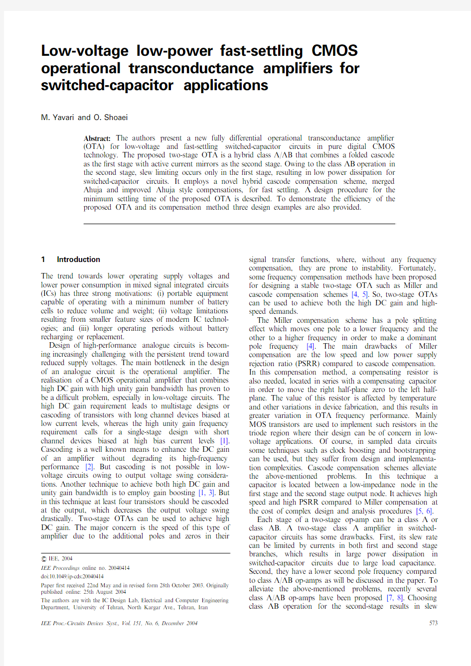
Figure 1shows the proposed OTA structure.The ?rst stage is a folded cascode ampli?er with PMOS input transistors.
The PMOS input differential pair allows the use of near ground V cmi ,as the op-amp input common mode voltage.This allows the use of relatively small NMOS transistors to design the switches that are connected to V cmi .This greatly increases the switch linearity in very low-voltage circuitry without any complex area and power consuming techniques such as bootstrapping and clock boosting.The second stage is a class AB ampli?er with active current mirrors similar to [7].The class AB operation of this stage ensures that slew limiting occurs only in the ?rst stage.The second stage current is chosen to set the non-dominant poles at an adequately high frequency to guarantee stability.Because of the push–pull operation,the lowest non-dominant pole in the class A/AB design is governed by the time constant formed by the approximate sum of transconductance of the output transistors,M4and M5and the parasitic capaci-tances at the ?rst stage output [5,7].Thus the output branch current can be about half that used in the two-stage class A circuit for the same non-dominant pole frequency.When this fact is exploited together with the use of gain in the second stage current mirrors,a signi?cant reduction in power dissipation can be achieved relative to the two-stage class A topology.The mirror pole and zero will eventually degrade the phase margin of the circuit and ?nally its settling performance.To increase the mirror pole and zero frequencies in the active current mirrors,NMOS transistors are used in this design,where their transconductance can be about three times greater than PMOS transistors with the
same overdrive voltages and gate dimensions due to the higher electron mobility compared to holes.
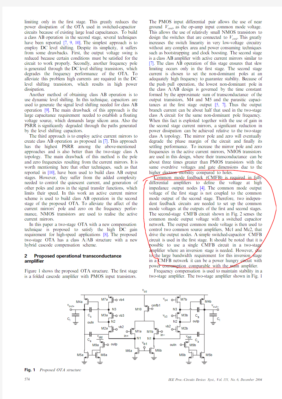
Common mode feedback (CMFB)is required in fully differential ampli?ers to de?ne the voltage at high impedance output nodes [4].The common mode output voltage of the ?rst stage is not coupled to the common mode output of the second stage.Therefore,two indepen-dent feedback circuits are needed to set up the common mode voltages at the outputs of the ?rst and second stages.The second-stage CMFB circuit shown in Fig.2senses the common mode output voltage with a switched capacitor network.The output common mode voltage is then used to control two common source ampli?ers,Mc1and Mc2,that drive the output nodes.A simple switched-capacitor CMFB circuit is used in the ?rst stage.It should be noted that it is possible to use a single CMFB circuit in a two-stage ampli?er where an inversion stage is needed.However,due to the large bandwidth requirement for this inversion stage in a CMFB network it can be a power hungry circuit with power consumption comparable with the main ampli?er.Frequency compensation is used to maintain stability in a two-stage ampli?er.The two-stage ampli?er shown in Fig.1
v dd
Fig.1
Proposed OTA structure
employs a novel cascode compensation scheme where two capacitors are used between two low-impedance nodes in the ?rst stage and the output node.In turn,this novel compensation approach merges Ahuja [5]and improved Ahuja style [11]compensation methods,to create two real poles,two complex poles at higher frequency,and three zeros.This compensation scheme yields a higher ampli?er bandwidth than the standard Miller and conventional cascode compensation techniques at the cost of a more complex design procedure for the settling behaviour of the ampli?er.Since the proposed compensation scheme creates an ampli?er with four closed-loop poles and three zeros,the design equations become signi?cantly more complicated than those of a single-stage OTA or conventional Miller and cascode compensated two-stage ampli?er.This implies that for practical designs some form of computer optimisa-tion constrained by trade-offs in the design equations will be necessary.
Figure 3shows the closed-loop small-signal equivalent circuit for pole and zero analysis of the proposed OTA shown in Fig.1,where C 1,C 2,C 3,and C L represent the parasitic capacitances of nodes N 1,N 2,N 3,and the output node of the circuit shown in Fig.1,respectively.f is the feedback factor.To simplify analysis,the output resistances of the devices are assumed to be in?nite.It should be noted that the effect of ?nite device resistance is to move the ampli?er poles slightly to the left,which will slightly increase the bandwidth of the ampli?er [12,13].The node equations of this circuit are as follows:
g m 1v 1tesC 1tg m 2Tv 2tsC a ev 2àv o T?0
e1TsC 2v 3àg m 2v 2àg m 3v 4?0e2TesC 3tg m 3tsC s Tv 4àsC s v o ?0e3TesC L tsC a tsC s Tv o àsC a v 2teg m 4tg m 5Tv 3àsC s v 4?0
e4Tv 1?v in àfv o
e5T
So,the transfer function will be:
v o v in
?
g m 1es 2C a C 2àg m 2g m Teg m 3tsC 3tsC s Ts 4d 4ts 3d 3ts 2d 2tsd 1td 0e6T
where
g m ?g m 4tg m 5
e7Td 4?C 2
a C 2eC 3tC s TtC 2s C 2eC 1tC a T
àC 2eC L tC a tC s TeC 1tC a TeC 3tC s T
e8T
d 3?C a C 2fg m 1eC 3tC s TtC 2a C 2g m 3tC 2C 2s g m 2
àg m 2C 2eC L tC a tC s TeC s tC 3T
àg m 3C 2eC L tC a tC s TeC 1tC a Te9T
d 2?fg m 1g m 3C a C 2àg m 2g m C a eC 3tC s T
àg m 3g m C s eC 1tC a Tàg m 2g m 3C 2eC L tC a tC s T
e10T
d 1?àfg m 1g m 2g m eC 3tC s Tàg m 2g m 3g m C a
àg m 2g m 3g m C s
e11Td 0?àfg m 1g m 2g m 3g m
e12T
To verify the usefulness of the proposed compensation
technique,the settling times of Ahuja style,improved Ahuja style,and the proposed compensation techniques are shown as functions of the total compensation capacitance in Fig.4.In these simulations the small-signal parameters shown in Table 1have been used.According to Fig.4,the proposed compensation technique gives a lower settling time than the other alternatives.
3
Design procedure
To investigate the settling behaviour of the proposed compensation technique a standard fourth-order system
?L
Fig.3Closed-loop small-signal equivalent circuit
3
4
5
6
7
8
5
total compensation capacitance, pF s e t t l i n g t i m e , n s
Fig.4
Settling time with different compensation techniques
v cmo2
v cm2
v cmo2
v Fig.2Second-stage CMFB circuit
Table 1:Small-signal parameters
Parameter Value Parameter Value g m14mA/V C 10.206pF g m2 4.7mA/V C 20.627pF g m3 4.2mA/V C 30.267pF g m4 5.7mA/V C L 4pF g m5
7.4mA/V
f
0.8
with the following transfer function is considered:H es T?
k ez 2p às 2
Tes tc T
es ta Tes tb Tes t2zo n s to n T
?
k eg 2z 2o 2n às 2Tes tz zo n Tn n n n e13T
where a ?azo n ,b ?bzo n ,c ?z zo n and z p ?gzo n .
There are six system parameters,a ,b ,g ,o n ,z and z in the transfer function.o n and z are called the natural frequency and damping factor,respectively.Figure 5shows a description of these six system parameters in terms of the location of poles and zeros of the proposed compensation technique in a practical implementation.
In switched-capacitor circuits,the step response deter-mines the ampli?er settling performance in the time domain [14].It can be shown that the step response of the above-mentioned fourth-order system is as follows:
s et T?A cl f 1àa 1?e àazo n t àa 2?e àbzo n t
ta 3?e àzo n t a 4?cos eo n t ?????????????1àz 2q T
àa 3?e àzo n t a 5?sin eo n t ?????????????1àz 2q T
g e14T
where A cl is the closed-loop gain and
a 1?
b ez àa T
z eb àa Te1à2az ta 2z Te15Ta 2?a ez àb T
z ea àb Te1à2bz tb z T
e16Ta 3?
abz
z e1à2az 2ta 2z 2Te1à2bz 2tb 2z 2T
e17T
a 4?àz z eea à1Te
b à1Tz 2à1tz 2T
teaz 2à1Tea tb à2Tz
e18T
a 5?fez z 2à1Teea à1Te
b à1Tz 2à1tz 2T
tz z 2e1àz 2Tea tb à2Tg 1
?????????????
1àz 2
p e19T
In the calculation of the step response it is assumed that g
tends to in?nity since in practical cases the right-and left-plane z p zero pair in the closed-loop transfer function will be at much higher frequencies than the other poles and zeros.The settling error
e s ?
s e1Tàs et s T
s e1T
is obtained as
e s ?a 1?e àazo n t s ta 2?e àbzo n t s
àa 3?e àzo n t s a 4?cos eo n t s ?????????????1àz 2q T
ta 3?e àzo n t s a 5?sin eo n t s ?????????????1àz 2q T
e20T
This equation is very complex to intuitively explain how to
choose the system parameters to optimise the settling error.Therefore,numerical calculations are used.Figure 6shows the settling error of the proposed compensation technique for different values of the system parameters.For example,the system parameters obtained for à120dB settling error are a ?0.95,z ?0.9,z ?0.9,b ?0.95,and o n t s ?17.
The system parameters obtained for a speci?c settling error in a de?ned time can be used to determine the device parameters using the following equations:
ea tb t2To n z ?
d 3
d 4
e21Te2ea tb Tz 2tabz 2t1To 2n ?d 2d 4
e22Teea tb Tz t2z 3ab To 3n ?
d 1d 4
e23Tabz 2o 4n ?d 0
d 4
e24Tz zo n ?
g m 3C s tC 3
e25T
In these equations,the system parameters,a ,b ,z ,z ,and o n are known.The load and compensation capacitances,C L ,C a ,and C s are determined based on circuit noise considerations.The parasitic capacitances,C 1,C 2,and C 3are related to the device sizes.Also,all device transconduc-tances can be determined by transistor size.So,these equations can be solved to determine device sizes using numerical calculations.However,these equations are very complex.In order to achieve a coarse design of the proposed op-amp,some approximations are considered to simplify solution of the above-mentioned equations and also give some practical insight.In (8)–(11)the parasitic capacitances,C 1,C 2,and C 3are assumed to be much less than the other capacitances.In this case,(21)–(25)reduce to the following relations:
ea tb t2To n z ?à
fg m 1C L
tg m 2eC L tC a T
C a C L t
g m 3eC L tC s T
C s C L
e26Te2ea tb Tz 2tabz 2t1To 2n ?à
fg m 1g m 3
C s C L
teg m 2tg m 3Tg m C 2C L
t
g m 2g m 3eC L tC a tC s TC a C s C L e27T
eea tb Tz t2z 3ab To 3n ?
fg m 1g m 2g m C 2C a C L
t
g m 2g m 3g m eC a tC s TC 2C a C s C L
e28Tabz 2o 4n ?
fg m 1g m 2g m 3g m C 2C a C s C L e29Tz zo n ?
g m 3
C s
e30
T
Fig.5Closed-loop pole and zero locations
In these equations,the transconductance of transistors M1,M2,M3,M4,and M5and the parasitic capacitance C 2at node N 2are unknown and can be obtained by solving them.Then one can run circuit level simulations to re?ne the gate dimensions obtained from system level calculations to achieve the desired performance.4
Simulation results
To demonstrate the usefulness of the proposed OTA and its
compensation technique,three different design examples with Ahuja style,improved Ahuja style,and the proposed compensation techniques were considered at the circuit level.First,the system parameters of these design examples were obtained using their settling error equations with numerical calculations using MATLAB [15].Then,circuits were simulated in a 0.25m m BSIM3v3level 49mixed-signal CMOS model with HSPICE.The threshold voltages for this technology for NMOS and PMOS transistors are 0.55V and à0.65V,respectively excluding the body effect.This process has 2-poly 5-metal (2P5M)form.Poly–poly capacitors are available in this technology to implement high linear capacitors.In these simulations,the OTAs were designed for a switched-capacitor integrator as shown in Fig.7.The bootstrapped switches proposed in [16]were used in these designs.Figure 8shows the settling behaviour of the proposed OTA with three different compensation methods.Simulation results are given in Table 2.Table 3
shows the OTA design parameters used in the HSPICE simulations.Simulation results in Fig.8show that the proposed cascode compensation technique results in a faster settling performance compared to the Ahuja and improved Ahuja style compensation methods with the same power consumption.It is worth mentioning that for designs of the proposed OTA with different compensation methods having the same settling time,the proposed cascode compensation technique results in lower power dissipation.Also the PSRR,slew rate,and input referred noise of the three compensation methods are approximately the same.
V v cmi v cmi
v v
Fig.7Switched-capacitor integrator
????s e t t l i n g e r r o r , d B
n t s c
n t s d
n t s b
n t s a
????????????s e t t l i n g e r r o r , d B
s e t t l i n g e r r o r , d B
s e t t l i n g e r r o r , d B
Fig.6
Settling errors as a function of o n t s
a For different values of z
b For different values of a
c For different values of z
d For different values of b
5Conclusions
In this paper a new merged two-stage class A/AB OTA has been proposed.Because of the class AB operation of the
second stage,the currents in this stage are determined so that the non-dominant poles and zeros are suf?ciently large in frequency to maintain stability.Thus,the second-stage currents are not constrained by the slew rate limiting of the OTA,which results in power saving in the switched-capacitor circuits.To move the mirror pole and zero to a high frequency,NMOS transistors are used in the active current mirrors.The op-amp employs a novel cascode compensation technique in which two compensating capacitors are used between two distinct low-impedance nodes of the ?rst stage and the output node of a two-stage OTA.This compensation approach results in faster settling performance than the conventional Miller,Ahuja style,and improved Ahuja style compensation techniques at the cost of a more complex design procedure.A design procedure was considered for the proposed OTA with its new compensation method.Circuit level simulations were also provided with HSPICE to demonstrate the ef?ciency of the proposed compensation technique.6
Acknowledgment
The authors would like to thank the anonymous reviewers of this manuscript for useful comments.This work was supported in part by a grant from the University of Tehran research budget under the contract number 612/3/816.7
References
1Gulati,K.,and Lee,H.-S.:‘A high-swing CMOS telescopic operational ampli?er’,IEEE J.Solid-State Circuits ,1998,33,(12),pp.2010–2019
2Johns,D.,and Martin,K.:‘Analog integrated circuit design’(John Wiley &Sons,1997)
3Bult,K.,and Geelen,G.J.G.M.:‘A fast-settling CMOS op-amp for SC circuits with 90-dB DC gain’,IEEE J.Solid-State Circuits ,1990,25,(6),pp.1379–1384
4Razavi,B.:‘Design of analog CMOS integrated circuits’(McGraw-Hill,2000)
5Ahuja,B.K.:‘An improved frequency compensation technique for CMOS operational ampli?ers’,IEEE J.Solid-State Circuits ,1983,18,(6),pp.629–633
6Ribner,D.B.,and Copeland,M.A.:‘Design techniques for cascoded CMOS op amps with improved PSRR and common-mode input range’,IEEE J.Solid-State Circuits ,1984,SC-19,(6),pp.919–9257Rabii,S.,and Wooley, B.A.:‘A 1.8-V digital-audio sigma-delta modulator in 0.8-m m CMOS’,IEEE J.Solid-State Circuits ,1997,32,(6),pp.783–796
8Yavari,M.,and Shoaei,O.:‘Low-voltage low-power fast-settling CMOS operational transconductance ampli?ers for switched-capaci-tor applications’.Proc.IEEE Int.Symp.on Low Power Electronics and Design,ISLPED,August 2003,pp.345–348
9Carvajal,R.G.,Torralba,A.,Ramirez-Angulo,J.,Tombs,J.,and Munoz,F.:‘Low-voltage class AB output stages for CMOS op-amps using ?oating capacitors’.Proc.IEEE Int.Symp.on Circuits and Systems,May 2001,Vol.1,pp.13–16
10Carvajal,R.G.,Torralba,A.,Ramirez-Angulo,J.,Tombs,J.,and
Munoz,F.:‘Low-voltage class AB output stages for CMOS op-amps’.Proc.28th European Solid-State Circuits Conf.,ESSCIRC,Sept.2002,pp.739–742
11Yao,L.,Steyaert,M.,and Sansen,W.:‘Fast-settling CMOS two-stage
operational transconductance ampli?ers and their systematic design’.Proc.IEEE Int.Symp.on Circuits and Systems,May 2002,Vol.2,pp.839–842
12Feldman,A.:‘High-speed,low-power sigma-delta modulators for RF
baseband channel applications’.PhD dissertation,University of California at Berkeley,1997
13Cline,D.:‘Noise,speed,and power trade-offs in pipelined analog to
digital converters’.PhD dissertation,University of California at Berkeley,1995
14Yang,H.C.,and Allstot, D.J.:‘Considerations on fast settling
operational ampli?ers’,IEEE Trans.Circuits Syst.,1990,37,(3),pp.326–334
15‘MATLAB and SIMULINK User’s Guides’(MathWorks,Inc.,2002)16Dessouky,M.,and Kaiser,A.:‘Very low-voltage digital audio DS
modulator with 88-dB dynamic range using local switch boot-strapping’,IEEE J.Solid-State Circuits ,2001,36,(3),pp.349–355
Table 2:Simulation results
Parameter
Ahuja
Improved Ahuja Proposed method Power supply voltage,V 1.5 1.5 1.5DC gain,dB
80.37980Unity gain bandwidth,MHz 137151167Phase margin,deg 75.58973.5Settling time (0.01%),ns 10.112.47.1Slew rate,V/m s 476487464Output swing,V pp 1.13 1.13
1.13
Input referred thermal
noise,V 2/Hz
1.6?10à16
1.5?10à16
1.2?10à16Power consumption,mW
8.9
8.9
8.9
Table 3:Device sizes used in HSPICE simulations
Parameter
Ahuja
Improved Ahuja Proposed method (W /L )180/0.580/0.5120/0.5(W /L )250/0.3570/0.3550/0.35(W /L )3180/0.35300/0.25150/0.35(W /L )4200/0.35200/0.35200/0.35(W /L )5100/0.35100/0.35100/0.35(W /L )680/0.580/0.580/0.5(W /L )7200/0.5200/0.5200/0.5(W /L )850/0.3550/0.3550/0.35(W /L )9100/0.35100/0.35100/0.35(W /L )10250/0.25250/0.25
250/0.25
C s ,pF F 3 1.5C a ,pF 3F 1.5C L ,pF
4
4
4
1
2
3
4
56
7
8
9
10
-0.4
-0.20
0.20.4
time, ns
v o l t a g e , V
Fig.8Transient simulation results (step response)