(3TPS62130,TPS62130A TPS62131,TPS62132,TPS62133
https://www.doczj.com/doc/c09837817.html, SLVSAG7B –NOVEMBER 2011–REVISED JUNE 2013
3-17V 3A Step-Down Converter in 3x3QFN Package
Check for Samples:TPS62130,TPS62130A ,TPS62131,TPS62132,TPS62133
FEATURES
DESCRIPTION The TPS6213X family is an easy to use synchronous ?DCS-Control TM Topology
step down DC-DC converter optimized for ?Input Voltage Range:3to 17V
applications with high power density.A high switching ?Up to 3A Output Current
frequency of typically 2.5MHz allows the use of small inductors and provides fast transient response as well ?Adjustable Output Voltage from 0.9to 6V
as high output voltage accuracy by utilization of the ?Pin-Selectable Output Voltage (nominal,+5%)
DCS-Control?topology.?Programmable Soft Start and Tracking
With its wide operating input voltage range of 3V to ?Seamless Power Save Mode Transition
17V,the devices are ideally suited for systems ?Quiescent Current of 17μA (typ.)
powered from either a Li-Ion or other batteries as well as from 12V intermediate power rails.It supports up ?Selectable Operating Frequency
to 3A continuous output current at output voltages ?Power Good Output
between 0.9V and 6V (with 100%duty cycle mode).?100%Duty Cycle Mode
The output voltage startup ramp is controlled by the ?Short Circuit Protection
soft-start pin,which allows operation as either a ?Over Temperature Protection
standalone power supply or in tracking configurations.Power sequencing is also possible by configuring the
?Available in a 3×3mm,QFN-16Package Enable and open-drain Power Good pins.
APPLICATIONS In Power Save Mode,the devices show quiescent
current of about 17μA from VIN.Power Save Mode,
?Standard 12V Rail Supplies entered automatically and seamlessly if load is small,
?POL Supply from Single or Multiple Li-Ion maintains high efficiency over the entire load range.
Battery In Shutdown Mode,the device is turned off and
?Solid-State Disk Drives shutdown current consumption is less than 2μA.
?Embedded Systems The device,available in adjustable and fixed output
voltage versions,is packaged in a 16-pin QFN
?
LDO replacement package measuring 3×3mm (RGT).?Mobile PC's,Tablet,Modems,Cameras
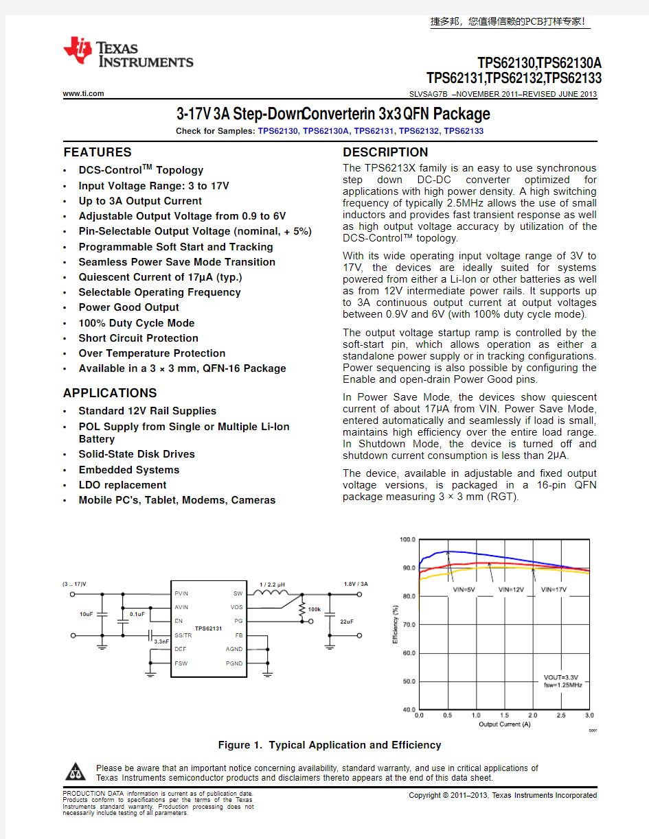
Figure 1.Typical Application and Efficiency
Please be aware that an important notice concerning availability,standard warranty,and use in critical applications of
捷多邦,您值得信赖的PCB打样专家!
TPS62130,TPS62130A
TPS62131,TPS62132,TPS62133
SLVSAG7B–NOVEMBER2011–REVISED https://www.doczj.com/doc/c09837817.html,
These devices have limited built-in ESD protection.The leads should be shorted together or the device placed in conductive foam during storage or handling to prevent electrostatic damage to the MOS gates.
ORDERING INFORMATION(1)
T A OUTPUT VOLTAGE PART NUMBER(2)PACKAGE ORDERING PACKAGE
MARKING adjustable TPS62130TPS62130RGT PTSI
adjustable TPS62130A(3)TPS62130ARGT PA6I -40°C to85°C 1.8V TPS6213116-Pin QFN TPS62131RGT QVX
3.3V TPS62132TPS62132RGT QVY
5.0V TPS62133TPS62133RGT QVZ
(1)For detailed ordering information please check the PACKAGE OPTION ADDENDUM section at the end of this datasheet.
(2)Contact the factory to check availability of other fixed output voltage versions.
(3)While TPS6213X has PG=High Z,TPS62130A features PG=Low,when device is in shutdown through EN,UVLO or Thermal Shutdown. ABSOLUTE MAXIMUM RATINGS(1)
over operating free-air temperature range(unless otherwise noted)
MIN MAX UNIT
AVIN,PVIN–0.320
V EN,SS/TR–0.3V IN+0.3
Pin voltage range(2)
SW–0.3V IN+0.3V
DEF,FSW,FB,PG,VOS–0.37V Power Good sink current PG10mA
Operating junction temperature range,T J–40125
Temperature range°C Storage temperature range,T stg–65150
HBM Human body model2kV ESD rating(3)
CDM Charge device model0.5kV (1)Stresses beyond those listed under absolute maximum ratings may cause permanent damage to the device.These are stress ratings
only,and functional operation of the device at these or any other conditions beyond those indicated under recommended operating conditions is not implied.Exposure to absolute-maximum-rated conditions for extended periods may affect device reliability.
(2)All voltages are with respect to network ground terminal.
(3)ESD testing is performed according to the respective JESD22JEDEC standard.
THERMAL INFORMATION
TPS6213X
THERMAL METRIC(1)UNITS
RGT16PINS
θJA Junction-to-ambient thermal resistance29.1
θJC(TOP)Junction-to-case(top)thermal resistance15
θJB Junction-to-board thermal resistance11
°C/W
ψJT Junction-to-top characterization parameter0.5
ψJB Junction-to-board characterization parameter10
θJC(BOTTOM)Junction-to-case(bottom)thermal resistance 3.5
(1)For more information about traditional and new thermal metrics,see the IC Package Thermal Metrics application report,SPRA953. RECOMMENDED OPERATING CONDITIONS
MIN TYP MAX UNIT Supply Voltage,V IN(at AVIN and PVIN)317V Operating free air temperature,T A–4085°C Operating junction temperature,T J–40125°C
2Submit Documentation Feedback Copyright?2011–2013,Texas Instruments Incorporated
TPS62130,TPS62130A
TPS62131,TPS62132,TPS62133 https://www.doczj.com/doc/c09837817.html, SLVSAG7B–NOVEMBER2011–REVISED JUNE2013 ELECTRICAL CHARACTERISTICS
over free-air temperature range(T A=-40°C to+85°C),typical values at V IN=12V and T A=25°C(unless otherwise noted)
PARAMETER TEST CONDITIONS MIN TYP MAX UNIT
SUPPLY
V IN Input voltage range(1)317V
I Q Operating quiescent current EN=High,I OUT=0mA,device not switching1725μA
I SD Shutdown current(2)EN=Low 1.54μA
V UVLO Falling Input Voltage 2.6 2.7 2.8V Undervoltage lockout threshold
Hysteresis200mV
T SD Thermal shutdown temperature160
°C Thermal shutdown hysteresis20
CONTROL(EN,DEF,FSW,SS/TR,PG)
High level input threshold voltage(EN,
V H0.9V DEF,FSW)
V L Low level input threshold voltage(EN,
0.3V
DEF,FSW)
I LKG Input leakage current(EN,DEF,FSW)EN=V IN or GND;DEF,FSW=V OUT or GND0.011μA
Rising(%V OUT)929598
V TH_PG Power good threshold voltage%
Falling(%V OUT)879094
V OL_PG Power good output low I PG=–2mA0.070.3V
I LKG_PG Input leakage current(PG)V PG=1.8V1400nA
I SS/TR SS/TR pin source current 2.3 2.5 2.7μA
POWER SWITCH
V IN≥6V90170 High-side MOSFET ON-resistance mΩ
V IN=3V120
R DS(ON)
V IN≥6V4070 Low-side MOSFET ON-resistance mΩ
V IN=3V50
I LIMF High-side MOSFET forward current limit(3)V IN=12V,T A=25°C 3.6 4.2 4.9A
OUTPUT
VREF Internal reference voltage(4)0.8V
I LKG_FB Input leakage current(FB)TPS62130,V FB=0.8V1100nA
Output voltage range(TPS62130)V IN≥V OUT0.9 6.0V
DEF(Output voltage programming)DEF=0(GND)VOUT
DEF=1(V OUT)VOUT+5%
PWM mode operation,V IN≥V OUT+1V–1.8 1.8
PWM mode operation,V IN≥V OUT+1V,
V OUT Initial output voltage accuracy(5)–1.5 1.6%
T A=–10°C to85°C
Power Save Mode operation,C OUT=22μF–2.3 2.8
Load regulation(6)V IN=12V,V OUT=3.3V,PWM mode operation0.05%/A
3V≤V IN≤17V,V OUT=3.3V,I OUT=1A,PWM0.02%/V Line regulation(6)
mode operation
(1)The device is still functional down to Under Voltage Lockout(see parameter V UVLO).
(2)Current into AVIN+PVIN pin.
(3)This is the static current limit.It can be temporarily higher in applications due to internal propagation delay(see Current Limit And Short
Circuit Protection section).
(4)This is the voltage regulated at the FB pin.
(5)This is the accuracy provided by the device itself(line and load regulation effects are not included).For the fixed voltage versions the
(internal)resistive divider is included.
(6)Line and load regulation depend on external component selection and layout(see Figure17and Figure18).
Copyright?2011–2013,Texas Instruments Incorporated Submit Documentation Feedback3
PVIN PVIN AVIN SS/TR SW
SW
SW
PG P G N D P G N D V O S
E N
F B A
G N D F S W
D E F TPS62130,TPS62130A TPS62131,TPS62132,TPS62133
SLVSAG7B –NOVEMBER 2011–REVISED JUNE https://www.doczj.com/doc/c09837817.html,
DEVICE INFORMATION
RGT PACKAGE
(TOP VIEW)
Terminal Functions
PIN
(1)I/O DESCRIPTION NAME
NO.SW
1,2,3O Switch node,which is connected to the internal MOSFET switches.Connect inductor between SW and output capacitor.PG
4O Output power good (High =VOUT ready,Low =VOUT below nominal regulation);open drain (requires pull-up resistor)FB
5I Voltage feedback of adjustable version.Connect resistive voltage divider to this pin.It is recommended to connect FB to AGND on fixed output voltage versions for improved thermal performance.AGND
6Analog Ground.Must be connected directly to the Exposed Thermal Pad and common ground plane.FSW
7I Switching Frequency Select (Low ≈2.5MHz,High ≈1.25MHz (2)for typical operation)(3)DEF
8I Output Voltage Scaling (Low =nominal,High =nominal +5%)(3)Soft-Start /Tracking Pin.An external capacitor connected to this pin sets the internal voltage reference rise SS/TR
9I time.It can be used for tracking and sequencing.AVIN
10I Supply voltage for control circuitry.Connect to same source as PVIN.PVIN
11,12I Supply voltage for power stage.Connect to same source as AVIN.EN
13I Enable input (High =enabled,Low =disabled)(3)VOS
14I Output voltage sense pin and connection for the control loop circuitry.PGND
15,16Power Ground.Must be connected directly to the Exposed Thermal Pad and common ground plane.Exposed
Must be connected to AGND (pin 6),PGND (pin 15,16)and common ground plane (4).Must be soldered to Thermal Pad
achieve appropriate power dissipation and mechanical reliability.(1)
For more information about connecting pins,see DETAILED DESCRIPTION and APPLICATION INFORMATION sections.(2)
Connect FSW to VOUT or PG in this case.(3)
An internal pull-down resistor keeps logic level low,if pin is floating.(4)See Figure 41.
4Submit Documentation Feedback Copyright ?2011–2013,Texas Instruments Incorporated
PVIN
PVIN
AVIN
PG
PGND PGND SW SW SW
EN*
SS/TR
DEF*
FSW*
VOS
FB
*This pin is connected to a pull down resistor internally
(see Detailed Description section).
TPS62130,TPS62130A TPS62131,TPS62132,TPS62133
https://www.doczj.com/doc/c09837817.html, SLVSAG7B–NOVEMBER2011–REVISED JUNE2013
FUNCTIONAL BLOCK DIAGRAM
Figure2.TPS62130(adjustable output voltage)
Copyright?2011–2013,Texas Instruments Incorporated Submit Documentation Feedback5
PVIN
PVIN AVIN PG PGND
PGND SW
SW
SW
EN *
SS/TR
DEF *
FSW *
VOS FB **This pin is connected to a pull down resistor internally
(see Detailed Description section).TPS62130,TPS62130A TPS62131,TPS62132,TPS62133
SLVSAG7B –NOVEMBER 2011–REVISED JUNE https://www.doczj.com/doc/c09837817.html,
Figure 3.TPS62131/2/3(fixed output voltage)
6Submit Documentation Feedback Copyright ?2011–2013,Texas Instruments Incorporated
TPS62130,TPS62130A TPS62131,TPS62132,TPS62133
https://www.doczj.com/doc/c09837817.html, SLVSAG7B –NOVEMBER 2011–REVISED JUNE 2013
PARAMETER MEASUREMENT INFORMATION
List of Components
REFERENCE
DESCRIPTION MANUFACTURER IC
17V,3A Step-Down Converter,QFN TPS62130RGT,Texas Instruments L1
2.2μH,0.165x 0.165in XFL4020-222MEB,Coilcraft Cin
10μF,25V,Ceramic Standard Cout
22μF,6.3V,Ceramic Standard
Cs
3300pF,25V,Ceramic R1
depending on Vout R2
depending on Vout R3100k Ω,Chip,0603,1/16W,1%Standard Figure 4.Measurement Setup
TYPICAL CHARACTERISTICS
Table of Graphs
DESCRIPTION
FIGURE Efficiency
vs output Current,vs Input Voltage 5–16vs Output Current (Load regulation),vs Input Voltage (Line Output voltage
17,18regulation)vs Input Voltage 19Switching Frequency
vs Output Current 20Quiescent Current
vs Input Voltage 21Shutdown Current
vs Input Voltage 22Power FET RDS(on)
vs Input Voltage (High-Side,Low-Side)23,24Output Voltage Ripple
vs Output Current 25Maximum Output Current
vs Input Voltage 26Power Supply Rejection Ratio
vs Frequency
27,28(PSSR)PWM-PSM-PWM Mode Transition
29Load Transient Response
30–32Waveforms Startup
33,34Typical PWM Mode Operation
35Typical Power Save Mode Operation
36vs Load Current
37Maximum Ambient Temperature vs Power Dissipation 38
Copyright ?2011–2013,Texas Instruments Incorporated Submit Documentation Feedback 7
0.010.0
20.0
30.0
40.0
50.060.070.080.0
90.0
100.0
Output Current (A)E f f i c i e n c y (%)G001
4567891011121314151617
Input Voltage (V)E f f i c i e n c y (%)
G001 0.010.0
20.0
30.0
40.050.060.070.080.0
90.0
100.0
Output Current (A)E f f i c i e n c y (%)
G001 7891011121314151617Input Voltage (V)
G001
0.010.0
20.0
30.0
40.0
50.060.070.080.0
90.0
100.0
Output Current (A)E f f i c i e n c y (%)
G001 78910111213
14151617Input Voltage (V)G001 TPS62130,TPS62130A TPS62131,TPS62132,TPS62133
SLVSAG7B –NOVEMBER 2011–REVISED JUNE https://www.doczj.com/doc/c09837817.html,
EFFICIENCY EFFICIENCY vs vs OUTPUT CURRENT INPUT VOLTAGE Figure 5.Efficiency with 1.25MHz,Vout=5V
Figure 6.Efficiency with 1.25MHz,Vout=5V EFFICIENCY EFFICIENCY vs vs Figure 7.Efficiency with 2.5MHz,Vout=5V
Figure 8.Efficiency with 2.5MHz,Vout=5V EFFICIENCY EFFICIENCY vs vs OUTPUT CURRENT INPUT VOLTAGE Figure 9.Efficiency with 1.25MHz,Vout=3.3V Figure 10.Efficiency with 1.25MHz,Vout=3.3V
8Submit Documentation Feedback Copyright ?2011–2013,Texas Instruments Incorporated
0.010.0
20.0
30.0
40.050.060.070.080.0
90.0
100.0
Output Current (A)E f f i c i e n c y (%)G001 0.010.020.030.040.0
50.060.070.080.0
90.0100.0
Input Voltage (V)E f f i c i e n c y (%)
G001
0.010.0
20.0
30.0
40.0
50.060.070.080.0
90.0
100.0
Output Current (A)E f f i c i e n c y (%)G001 0.0
10.020.030.040.050.060.070.080.090.0100.0
Input Voltage (V)E f f i c i e n c y (%)
G001 0.010.0
20.0
30.0
40.050.060.070.080.0
90.0
100.0
Output Current (A)E f f i c i e n c y (%)G001
Input Voltage (V)E f f i c i e n c y (%)G001
TPS62130,TPS62130A TPS62131,TPS62132,TPS62133
https://www.doczj.com/doc/c09837817.html, SLVSAG7B –NOVEMBER 2011–REVISED JUNE 2013
EFFICIENCY EFFICIENCY vs vs OUTPUT CURRENT INPUT VOLTAGE Figure 11.Efficiency with 2.5MHz,Vout=3.3V
Figure 12.Efficiency with 2.5MHz,Vout=3.3V EFFICIENCY EFFICIENCY vs vs OUTPUT CURRENT INPUT VOLTAGE Figure 13.Efficiency with 1.25MHz,Vout=1.8V
Figure 14.Efficiency with 1.25MHz,Vout=1.8V EFFICIENCY EFFICIENCY vs vs OUTPUT CURRENT INPUT VOLTAGE Figure 15.Efficiency with 1.25MHz,Vout=0.9V Figure 16.Efficiency with 1.25MHz,Vout=0.9V
Copyright ?2011–2013,Texas Instruments Incorporated Submit Documentation Feedback 9
0.05.0
10.0
15.020.025.030.035.040.0
45.0
50.0
Input Voltage (V)I n p u t C u r r e n t (μA )G001 0.00.51.01.5
2.02.5
3.03.5
4.04.5
5.0
Input Voltage (V)I n p u t C u r r e n t (μA )G001
00.5
1
1.52
2.53
3.5
4
Input Voltage (V)S w i t c h i n g F r e q u e n c y (M H z )
G000 0
0.511.522.533.54Output Current (A)S w i t c h i n g F r e q u e n c y (M H z )
G000 3.203.253.303.353.40Output Current (A)O u t p u t V o l t a g e (V )
G001 O u t p u t V o l t a g e (V )TPS62130,TPS62130A TPS62131,TPS62132,TPS62133
SLVSAG7B –NOVEMBER 2011–REVISED JUNE https://www.doczj.com/doc/c09837817.html,
OUTPUT VOLTAGE OUTPUT VOLTAGE vs vs OUTPUT CURRENT INPUT VOLTAGE
Figure 17.Output Voltage Accuracy (Load Regulation)
SWITCHING FREQUENCY SWITCHING FREQUENCY vs vs INPUT VOLTAGE OUTPUT CURRENT Figure 19.Switching Frequency
Figure 20.Switching Frequency INPUT CURRENT INPUT CURRENT vs vs INPUT VOLTAGE INPUT VOLTAGE Figure 21.Quiescent Current Figure 22.Shutdown Current
10Submit Documentation Feedback Copyright ?2011–2013,Texas Instruments Incorporated
010
20
30
40
5060708090100
Frequency (Hz)P S R R (d B )G000 0102030405060708090
100Frequency (Hz)P S R R (d B )G000
00.010.020.030.040.05
Output Current (A)O u t p u t V o l t a g e R i p p l e (V )G000
Input Voltage (V)O u t p u t C u r r e n t (A )
G000 0.020.0
40.0
60.080.0100.0120.0140.0160.0180.0
200.0
Input Voltage (V)R D S o n H i g h ?S i d e (m ?)
G001 0.020.040.060.080.0100.0Input Voltage (V)R D S o n L o w ?S i d e (m ?)G001
TPS62130,TPS62130A TPS62131,TPS62132,TPS62133
https://www.doczj.com/doc/c09837817.html, SLVSAG7B –NOVEMBER 2011–REVISED JUNE 2013
STATIC DRAIN-SOURCE-RESISTANCE (R DSon )STATIC DRAIN-SOURCE-RESISTANCE (R DSon )vs vs INPUT VOLTAGE Figure 23.High-Side Switch Resistance
Figure 24.Low-Side Switch Resistance OUTPUT VOLTAGE OUTPUT CURRENT vs vs OUTPUT CURRENT
INPUT VOLTAGE Figure 25.Output Voltage Ripple
Figure 26.Maximum Output Current POWER SUPPLY REJECTION RATIO POWER SUPPLY REJECTION RATIO vs vs FREQUENCY
FREQUENCY Figure 27.Power Supply Rejection Ratio,f SW =2.5MHz Figure 28.Power Supply Rejection Ratio,f SW =2.5MHz
Copyright ?2011–2013,Texas Instruments Incorporated Submit Documentation Feedback 11
TPS62130,TPS62130A TPS62131,TPS62132,TPS62133
SLVSAG7B –NOVEMBER 2011–REVISED JUNE https://www.doczj.com/doc/c09837817.html,
OUTPUT VOLTAGE OUTPUT VOLTAGE vs vs TIME TIME
Figure 29.PWM-PSM-Transition (V IN =12V,V OUT =3.3V with Figure 30.Load Transient Response (I OUT =0.5to 3to 0.5A,50mV/div)
V IN =12V,V OUT =3.3V)OUTPUT VOLTAGE OUTPUT VOLTAGE vs vs TIME TIME
Figure 31.Load Transient Response of Figure 30,rising Figure 32.Load Transient Response of Figure 30,falling edge edge
12Submit Documentation Feedback Copyright ?2011–2013,Texas Instruments Incorporated
TPS62130,TPS62130A
TPS62131,TPS62132,TPS62133 https://www.doczj.com/doc/c09837817.html, SLVSAG7B–NOVEMBER2011–REVISED JUNE2013
OUTPUT VOLTAGE OUTPUT VOLTAGE
vs vs
TIME TIME
Figure33.Startup into100mA(VIN=12V,VOUT=3.3V)Figure34.Startup into3A(VIN=12V,VOUT=3.3V)
PWM SIGNALS POWER SAVE MODE SIGNALS
vs vs
TIME TIME
Figure35.Typical Operation in PWM Mode(I OUT=1A)Figure36.Typical Operation in Power Save Mode
(I OUT=10mA)
Copyright?2011–2013,Texas Instruments Incorporated Submit Documentation Feedback13
5565
75
85
95
105
115
125
Output Current (A)F r e e ?A i r T e m p e r a t u r e (°C )G000 5565758595105115
125Output Power (W)F r e e ?A i r T e m p e r a t u r e (°C )G000
TPS62130,TPS62130A TPS62131,TPS62132,TPS62133
SLVSAG7B –NOVEMBER 2011–REVISED JUNE https://www.doczj.com/doc/c09837817.html,
AMBIENT TEMPERATURE AMBIENT TEMPERATURE vs vs OUTPUT CURRENT OUTPUT POWER Figure 37.Maximum Ambient Temperature (f SW =2.5MHz)Figure 38.Maximum Ambient Temperature (f SW =2.5MHz)
14Submit Documentation Feedback Copyright ?2011–2013,Texas Instruments Incorporated
ON OUT IN peak LPSM t L V V I ×-=)()(ns V V t IN OUT ON 400×=TPS62130,TPS62130A TPS62131,TPS62132,TPS62133
https://www.doczj.com/doc/c09837817.html, SLVSAG7B –NOVEMBER 2011–REVISED JUNE 2013
DETAILED DESCRIPTION
Device Operation
The TPS6213X synchronous switched mode power converters are based on DCS-Control?(D irect C ontrol with
S eamless Transition into Power Save Mode),an advanced regulation topology,that combines the advantages of
hysteretic,voltage mode and current mode control including an AC loop directly associated to the output voltage.
This control loop takes information about output voltage changes and feeds it directly to a fast comparator stage.
It sets the switching frequency,which is constant for steady state operating conditions,and provides immediate
response to dynamic load changes.To get accurate DC load regulation,a voltage feedback loop is used.The
internally compensated regulation network achieves fast and stable operation with small external components
and low ESR capacitors.
The DCS-Control TM topology supports PWM (Pulse Width Modulation)mode for medium and heavy load
conditions and a Power Save Mode at light loads.During PWM,it operates at its nominal switching frequency in
continuous conduction mode.This frequency is typically about 2.5MHz with a controlled frequency variation
depending on the input voltage.If the load current decreases,the converter enters Power Save Mode to sustain
high efficiency down to very light loads.In Power Save Mode the switching frequency decreases linearly with the
load current.Since DCS-Control TM supports both operation modes within one single building block,the transition
from PWM to Power Save Mode is seamless without effects on the output voltage.
Fixed output voltage versions provide smallest solution size and lowest current consumption,requiring only 3
external components.An internal current limit supports nominal output currents of up to 3A.
The TPS6213X family offers both excellent DC voltage and superior load transient regulation,combined with
very low output voltage ripple,minimizing interference with RF circuits.
Pulse Width Modulation (PWM)Operation
The TPS6213X operates with pulse width modulation in continuous conduction mode (CCM)with a nominal
switching frequency of 2.5MHz or 1.25MHz,selectable with the FSW pin.The frequency variation in PWM is
controlled and depends on V IN ,V OUT and the inductance.The device operates in PWM mode as long the output
current is higher than half the inductor's ripple current.To maintain high efficiency at light loads,the device
enters Power Save Mode at the boundary to discontinuous conduction mode (DCM).This happens if the output
current becomes smaller than half the inductor's ripple current.
Power Save Mode Operation
The TPS6213X's built in Power Save Mode will be entered seamlessly,if the load current decreases.This
secures a high efficiency in light load operation.The device remains in Power Save Mode as long as the inductor
current is discontinuous.
In Power Save Mode the switching frequency decreases linearly with the load current maintaining high efficiency.
The transition into and out of Power Save Mode happens within the entire regulation scheme and is seamless in
both directions.
TPS6213X includes a fixed on-time circuitry.This on-time,in steady-state operation,can be estimated as:
(1)
For very small output voltages,an absolute minimum on-time of about 80ns is kept to limit switching losses.The
operating frequency is thereby reduced from its nominal value,which keeps efficiency https://www.doczj.com/doc/c09837817.html,ing t ON ,the typical
peak inductor current in Power Save Mode can be approximated by:
(2)
When V IN decreases to typically 15%above VOUT,the TPS6213X won't enter Power Save Mode,regardless of
the load current.The device maintains output regulation in PWM mode.
Copyright ?2011–2013,Texas Instruments Incorporated Submit Documentation Feedback 15
()
L )on (DS OUT (min)OUT (min)IN R R I V V ++=TPS62130,TPS62130A TPS62131,TPS62132,TPS62133
SLVSAG7B –NOVEMBER 2011–REVISED JUNE https://www.doczj.com/doc/c09837817.html,
100%Duty-Cycle Operation
The duty cycle of the buck converter is given by D=Vout/Vin and increases as the input voltage comes close to
the output voltage.In this case,the device starts 100%duty cycle operation turning on the high-side switch
100%of the time.The high-side switch stays turned on as long as the output voltage is below the internal set
point.This allows the conversion of small input to output voltage differences,e.g.for longest operation time of
battery-powered applications.In 100%duty cycle mode,the low-side FET is switched off.
The minimum input voltage to maintain output voltage regulation,depending on the load current and the output
voltage level,can be calculated as:
(3)
where
I OUT is the output current,
R DS(on)is the R DS(on)of the high-side FET and
R L is the DC resistance of the inductor used.Enable /Shutdown (EN)
When Enable (EN)is set High,the device starts operation.Shutdown is forced if EN is pulled Low with a
shutdown current of typically 1.5μA.During shutdown,the internal power MOSFETs as well as the entire control
circuitry are turned off.The internal resistive divider pulls down the output voltage smoothly.The EN signal must
be set externally to High or Low.An internal pull-down resistor of about 400k Ωis connected and keeps EN logic
low,if Low is set initially and then the pin gets floating.It is disconnected if the pin is set High.
Connecting the EN pin to an appropriate output signal of another power rail provides sequencing of multiple
power rails.
Soft Start /Tracking (SS/TR)
The internal soft start circuitry controls the output voltage slope during startup.This avoids excessive inrush
current and ensures a controlled output voltage rise time.It also prevents unwanted voltage drops from high-
impedance power sources or batteries.When EN is set to start device operation,the device starts switching after
a delay of about 50μs and VOUT rises with a slope controlled by an external capacitor connected to the SS/TR
pin.See Figure 33and Figure 34for typical startup operation.
Connecting SS/TR directly to AVIN provides fastest startup behavior.The TPS6213X can start into a pre-biased
output.During monotonic pre-biased startup,both the power MOSFETs are not allowed to turn on until the
device's internal ramp sets an output voltage above the pre-bias voltage.As long as the output is below about
0.5V a reduced current limit of typically 1.6A is set internally.If the device is set to shutdown (EN=GND),
undervoltage lockout or thermal shutdown,an internal resistor pulls the SS/TR pin down to ensure a proper low
level.Returning from those states causes a new startup sequence as set by the SS/TR connection.
A voltage supplied to SS/TR can be used for tracking a master voltage.The output voltage will follow this voltage
in both directions up and down (see APPLICATION INFORMATION ).
Current Limit And Short Circuit Protection
The TPS6213X devices are protected against heavy load and short circuit events.If a short circuit is detected
(VOUT drops below 0.5V),the current limit is reduced to 1.6A typically.If the output voltage rises above 0.5V,
the device will run in normal operation again.At heavy loads,the current limit determines the maximum output
current.If the current limit is reached,the high-side FET will be turned off.Avoiding shoot through current,the
low-side FET will be switched on to sink the inductor current.The high-side FET will turn on again,only if the
current in the low-side FET has decreased below the low side current limit threshold.
The output current of the device is limited by the current limit (see ELECTRICAL CHARACTERISTICS ).Due to
internal propagation delay,the actual current can exceed the static current limit during that time.The dynamic
current limit can be calculated as follows:
16Submit Documentation Feedback Copyright ?2011–2013,Texas Instruments Incorporated
()ns L V V I I OUT IN LIMF typ peak 30)(×-+
=PD L LIMF typ peak t L V I I ×+=)(TPS62130,TPS62130A TPS62131,TPS62132,TPS62133
https://www.doczj.com/doc/c09837817.html, SLVSAG7B –NOVEMBER 2011–REVISED JUNE 2013
(4)
where
I LIMF is the static current limit,specified in the ELECTRICAL CHARACTERISTICS ,
L is the inductor value,
V L is the voltage across the inductor (V IN -V OUT )and
t PD is the internal propagation delay.
The current limit can exceed static values,especially if the input voltage is high and very small inductances are
used.The dynamic high side switch peak current can be calculated as follows:
(5)
Power Good (PG)The TPS6213X has a built in power good (PG)function to indicate whether the output voltage has reached its
appropriate level or not.The PG signal can be used for startup sequencing of multiple rails.The PG pin is an
open-drain output that requires a pull-up resistor (to any voltage below 7V).It can sink 2mA of current and
maintain its specified logic low level.With TPS62130it is high impedance when the device is turned off due to
EN,UVLO or thermal shutdown.TPS62130A features PG=Low in this case and can be used to actively
discharge Vout (see Figure 51).VIN must remain present for the PG pin to stay Low.
Pin-Selectable Output Voltage (DEF)
The output voltage of the TPS6213X devices can be increased by 5%above the nominal voltage by setting the
DEF pin to High (1).When DEF is Low,the device regulates to the nominal output voltage.Increasing the nominal
voltage allows adapting the power supply voltage to the variations of the application hardware.More detailed
information on voltage margining using TPS6213X can be found in SLVA489.A pull down resistor of about
400kOhm is internally connected to the pin,to ensure a proper logic level if the pin is high impedance or floating
after initially set to Low.The resistor is disconnected if the pin is set High.
Frequency Selection (FSW)
To get high power density with very small solution size,a high switching frequency allows the use of small
external components for the output filter.However switching losses increase with the switching frequency.If
efficiency is the key parameter,more than solution size,the switching frequency can be set to half (1.25MHz
typ.)by pulling FSW to High.It is mandatory to start with FSW=Low to limit inrush current,which can be done by
connecting to VOUT or PG.Running with lower frequency a higher efficiency,but also a higher output voltage
ripple,is achieved.Pull FSW to Low for high frequency operation (2.5MHz typ.).To get low ripple and full output
current at the lower switching frequency,it's recommended to use an inductor of at least 2.2uH.The switching
frequency can be changed during operation,if needed.A pull down resistor of about 400kOhm is internally
connected to the pin,acting the same way as at the DEF Pin (see above).
Under Voltage Lockout (UVLO)
If the input voltage drops,the under voltage lockout prevents misoperation of the device by switching off both the
power FETs.The under voltage lockout threshold is set typically to 2.7V.The device is fully operational for
voltages above the UVLO threshold and turns off if the input voltage trips the threshold.The converter starts
operation again once the input voltage exceeds the threshold by a hysteresis of typically 200mV.
Thermal Shutdown
The junction temperature (Tj)of the device is monitored by an internal temperature sensor.If Tj exceeds 160°C
(typ),the device goes into thermal shut down.Both the high-side and low-side power FETs are turned off and PG
goes high impedance.When Tj decreases below the hysteresis amount,the converter resumes normal
operation,beginning with Soft Start.To avoid unstable conditions,a hysteresis of typically 20°C is implemented
on the thermal shut down temperature.
(1)Maximum allowed voltage is 7V.Therefore it's recommended to connect it to VOUT or PG,not VIN.
Copyright ?2011–2013,Texas Instruments Incorporated
Submit Documentation Feedback 17
2(max)
(max)(max)L OUT L I I I D +=÷÷????è?-=121REF OUT V V R R TPS62130,TPS62130A TPS62131,TPS62132,TPS62133
SLVSAG7B –NOVEMBER 2011–REVISED JUNE https://www.doczj.com/doc/c09837817.html,
APPLICATION INFORMATION
The following information is intended to be a guideline through the individual power supply design process.
Programming The Output Voltage
While the output voltage of the TPS62130is adjustable,the TPS62131/2/3are programmed to fixed output
voltages.For fixed output versions,the FB pin is pulled down internally and may be left floating.It is
recommended to connect to AGND to improve thermal resistance.The adjustable version can be programmed
for output voltages from 0.9V to 6V by using a resistive divider from VOUT to AGND.The voltage at the FB pin is
regulated to 800mV.The value of the output voltage is set by the selection of the resistive divider from
Equation 6(see Figure 4).It is recommended to choose resistor values which allow a current of at least 2uA,
meaning the value of R2shouldn't exceed 400k Ω.Lower resistor values are recommended for highest accuracy
and most robust design.For applications requiring lowest current consumption,the use of fixed output voltage
versions is recommended.
(6)
In case the FB pin gets opened,the device clamps the output voltage at the VOS pin internally to about 7.4V.
External Component Selection
The external components have to fulfill the needs of the application,but also the stability criteria of the devices
control loop.The TPS6213X is optimized to work within a range of external components.The LC output filters
inductance and capacitance have to be considered together,creating a double pole,responsible for the corner
frequency of the converter (see Output Filter And Loop Stability ).Table 1can be used to simplify the output filter
component selection.
Table 1.Recommended LC Output Filter Combinations (1)
4.7μF
10μF 22μF 47μF 100μF 200μF 400μF
0.47μH
1μH
√√√√2.2μH
√√(2)√√√3.3μH
√√√√4.7μH
(1)
The values in the table are nominal values.(2)This LC combination is the standard value and recommended for most applications.The TPS6213X can be run with an inductor as low as 1μH.FSW should be set Low in this case.However,for
applications running with the low frequency setting (FSW=High)or with low input voltages, 2.2μH is
recommended.More detailed information on further LC combinations can be found in SLVA463.
Inductor Selection
The inductor selection is affected by several effects like inductor ripple current,output ripple voltage,PWM-to-
PSM transition point and efficiency.In addition,the inductor selected has to be rated for appropriate saturation
current and DC resistance (DCR).Equation 7and Equation 8calculate the maximum inductor current under
static load conditions.
(7)
18Submit Documentation Feedback Copyright ?2011–2013,Texas Instruments Incorporated
L PSM load I I D =21)(÷÷÷÷÷???????è?×-×=D SW IN OUT OUT L f L V V V I (min)(max)(max)1TPS62130,TPS62130A TPS62131,TPS62132,TPS62133
https://www.doczj.com/doc/c09837817.html, SLVSAG7B –NOVEMBER 2011–REVISED JUNE 2013
(8)
where
I L (max)is the maximum inductor current,
ΔI L is the Peak to Peak Inductor Ripple Current,
L(min)is the minimum effective inductor value and
f SW is the actual PWM Switchin
g Frequency.
Calculating the maximum inductor current using the actual operating conditions gives the minimum saturation
current of the inductor needed.A margin of about 20%is recommended to add.A larger inductor value is also
useful to get lower ripple current,but increases the transient response time and size as well.The following
inductors have been used with the TPS6213X and are recommended for use:
Table 2.List of Inductors
Type
Inductance [μH]Current [A](1)Dimensions [LxBxH]MANUFACTURER mm XFL4020-102ME_
1.0μH,±20% 4.74x 4x
2.1Coilcraft XFL4020-152ME_
1.5μH,±20% 4.24x 4x
2.1Coilcraft XFL4020-222ME_
2.2μH,±20%
3.84x 4x 2.1Coilcraft IHLP1212BZ-11
1.0μH,±20% 4.53x 3.6x 2Vishay IHLP1212BZ-11
2.2μH,±20%
3.03x 3.6x 2Vishay SRP4020-3R3M
3.3μH,±20% 3.3
4.8x 4x 2Bourns VLC5045T-3R3N
3.3μH,±30%
4.05x 5x 4.5TDK (1)Lower of I RMS at 40°C rise or I SAT at 30%drop.
The inductor value also determines the load current at which Power Save Mode is entered:
(9)
Using Equation 8,this current level can be adjusted by changing the inductor value.
Capacitor Selection
Output Capacitor
The recommended value for the output capacitor is 22uF.The architecture of the TPS6213X allows the use of
tiny ceramic output capacitors with low equivalent series resistance (ESR).These capacitors provide low output
voltage ripple and are recommended.To keep its low resistance up to high frequencies and to get narrow
capacitance variation with temperature,it's recommended to use X7R or X5R https://www.doczj.com/doc/c09837817.html,ing a higher value can
have some advantages like smaller voltage ripple and a tighter DC output accuracy in Power Save Mode (see
SLVA463).
Note:In power save mode,the output voltage ripple depends on the output capacitance,its ESR and the peak
inductor https://www.doczj.com/doc/c09837817.html,ing ceramic capacitors provides small ESR and low ripple.
Copyright ?2011–2013,Texas Instruments Incorporated Submit Documentation Feedback 19
[V]
VSS/TR
[V]TR SS FB V V /64.0×?[]
F V A t C SS SS 25152..m ×=TPS62130,TPS62130A TPS62131,TPS62132,TPS62133
SLVSAG7B –NOVEMBER 2011–REVISED JUNE https://www.doczj.com/doc/c09837817.html,
Input Capacitor
For most applications,10μF will be sufficient and is recommended,though a larger value reduces input current
ripple further.The input capacitor buffers the input voltage for transient events and also decouples the converter
from the supply.A low ESR multilayer ceramic capacitor is recommended for best filtering and should be placed
between PVIN and PGND as close as possible to those pins.Even though AVIN and PVIN must be supplied
from the same input source,it's required to place a capacitance of 0.1uF from AVIN to AGND,to avoid potential
noise coupling.An RC,low-pass filter from PVIN to AVIN may be used but is not required.
Soft Start Capacitor
A capacitance connected between SS/TR pin and AGND allows a user programmable start-up slope of the
output voltage.A constant current source supports 2.5μA to charge the external capacitance.The capacitor
required for a given soft-start ramp time for the output voltage is given by:
(10)
where
C SS is the capacitance (F)required at the SS/TR pin and
t SS is the desired soft-start ramp time (s).
NOTE
DC Bias effect:High capacitance ceramic capacitors have a DC Bias effect,which will
have a strong influence on the final effective capacitance.Therefore the right capacitor
value has to be chosen carefully.Package size and voltage rating in combination with
dielectric material are responsible for differences between the rated capacitor value and
the effective capacitance.
Tracking Function
If a tracking function is desired,the SS/TR pin can be used for this purpose by connecting it to an external
tracking voltage.The output voltage tracks that voltage.If the tracking voltage is between 50mV and 1.2V,the
FB pin will track the SS/TR pin voltage as described in Equation 11and shown in Figure 39.
(11)
Figure 39.Voltage Tracking Relationship
20Submit Documentation Feedback Copyright ?2011–2013,Texas Instruments Incorporated