
RU30L15H
P-Channel Advanced Power MOSFET
MOSFET Features Pin Description
Applications
Symbol Parameter Rating Unit Common Ratings(T A=25°C Unless Otherwise Noted)
V DSS Drain-Source Voltage-30
V GSS Gate-Source Voltage±20
V T J Maximum Junction Temperature150°C
T STG Storage Temperature Range-55 to 150°C
I S Diode Continuous Forward Current T C=25°C-14.5A Mounted on Large Heat Sink
I DP300μs Pulse Drain Current Tested T
C
=25°C-58①A
T C=25°C-14.5
I D Continuous Drain Current
T C=70°C-11
A
T C=25°C 3.1
P D Maximum Power Dissipation
T C=70°C 2.0
W RθJA
②Thermal Resistance-Junction to Ambient40°C/W ?-30V/-14.5A,
R DS (ON)=13m? (Type)@V GS=-10V
R DS (ON)=22m? (Type)@V GS=-4.5V
?Super High Dense Cell Design
?Reliable and Rugged
?ESD Protected
?Lead Free and Green Available
?Load Switching.
?PWM Applications.
Absolute Maximum Ratings
SOP-8
P-Channel MOSFET
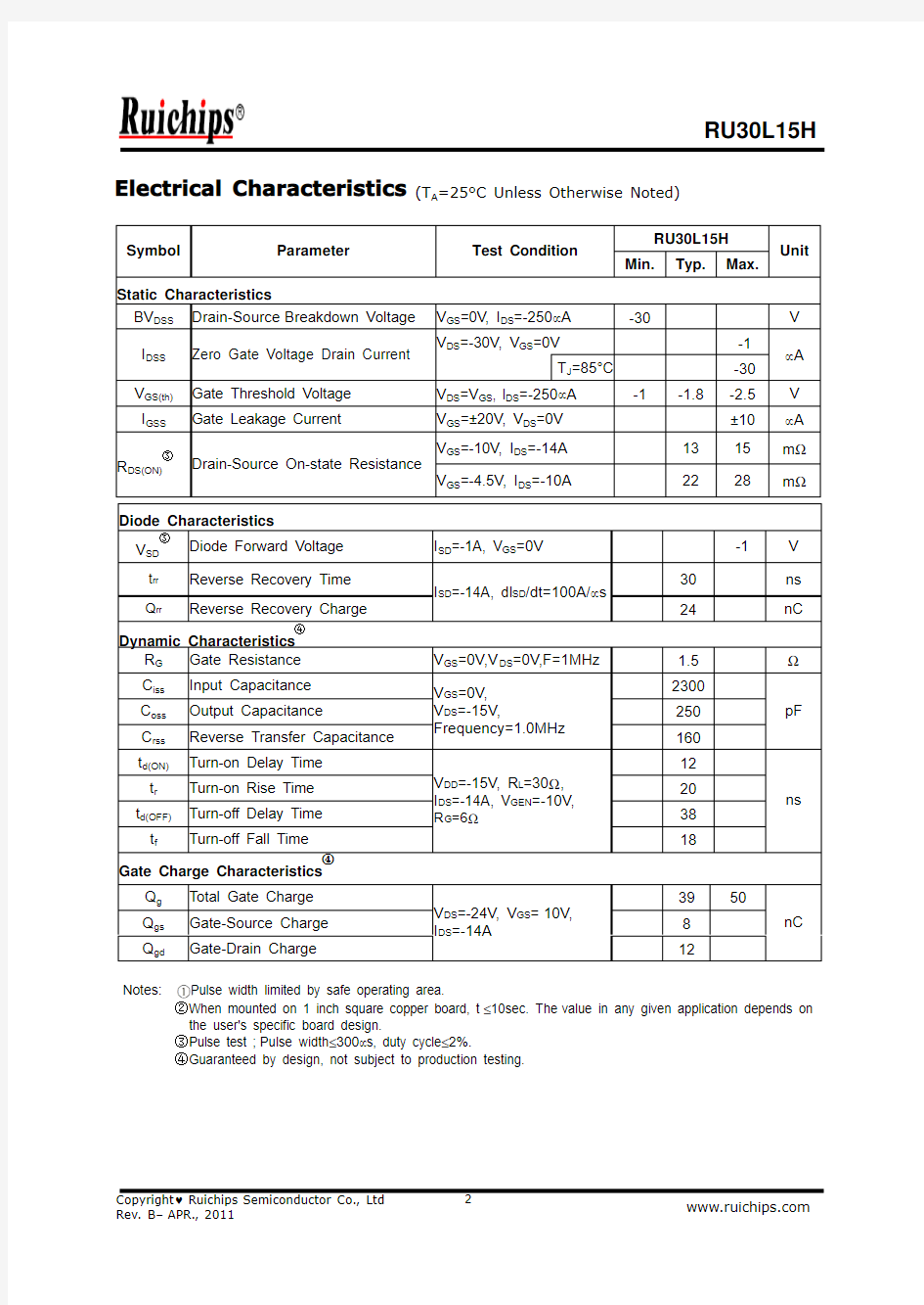
Electrical Characteristics
(T A =25°C Unless Otherwise Noted)
RU30L15H Symbol
Parameter Test Condition Min.
Typ.
Max.
Unit
Static Characteristics BV DSS Drain-Source Breakdown Voltage V GS =0V, I DS =-250μA -30
V V DS =-30V, V GS =0V
-1I DSS Zero Gate Voltage Drain Current T J =85°C
-30
μA V GS(th)Gate Threshold Voltage V DS =V GS , I DS =-250μA -1
-1.8
-2.5V I GSS Gate Leakage Current
V GS =±20V, V DS =0V ±10
μA V GS =-10V, I DS =-14A 1315m ?R DS(ON)
③
Drain-Source On-state Resistance
V GS =-4.5V, I DS =-10A
22
28
m ?
Notes:
Pulse width limited by safe operating area.
②When mounted on 1 inch square copper board, t ≤10sec. The value in any given application depends on the user's specific board design.
③Pulse test ;Pulse width ≤300μs, duty cycle ≤2%.
④Guaranteed by design, not subject to production testing.
Diode Characteristics V SD
③
Diode Forward Voltage I SD =-1A, V GS =0V
-1V t rr Reverse Recovery Time 30ns Q rr
Reverse Recovery Charge
I SD =-14A, dl SD /dt=100A/μs
24
nC Dynamic Characteristics
④
R G Gate Resistance
V GS =0V,V DS =0V,F=1MHz 1.5?C iss Input Capacitance 2300C oss Output Capacitance
250C rss Reverse Transfer Capacitance V GS =0V,V DS =-15V,
Frequency=1.0MHz
160pF
t d(ON)Turn-on Delay Time 12
t r Turn-on Rise Time 20t d(OFF)Turn-off Delay Time 38t f
Turn-off Fall Time
V DD =-15V, R L =30?,I DS =-14A, V GEN =-10V,R G =6?
18
ns
Gate Charge Characteristics
④
Q g Total Gate Charge 3950
Q gs Gate-Source Charge 8Q gd
Gate-Drain Charge
V DS =-24V, V GS =10V,
I DS =-14A
12
nC
Typical Characteristics
Power Dissipation Drain Current
P t
o
t
-
P
o
w
e
r
(
W
)
-
I
D
-
D
r
a
i
n
C
u
r
r
e
n
t
(
A
)
T j- Junction Temperature(°C)T j- Junction Temperature(°C) Safe Operation Area Thermal Transient Impedance
-
I
D
-
D
r
a
i
n
C
u
r
r
e
n
t
(
A
)
N
o
r
m
a
l
i
z
e
d
E
f
f
e
c
t
i
v
e
T
r
a
n
s
i
e
n
t
-V DS- Drain-Source Voltage(V)Square Wave Pulse Duration(sec)
Typical Characteristics
Output Characteristics
Drain-Source On Resistance
-I D - D r a i n C u r r e n t (A )
R D S (O N )- O n R e s i s t a n c e (m Ω)
-V DS - Drain-Source Voltage (V)
-I D -Drain Current (A)
Drain-Source On Resistance Gate Threshold Voltage
R D S (O N )- O n - R e s i s t a n c e (m )
N o r m a l i z e d T h r e s h o l d V o l t a g e
-V GS -Gate-Source Voltage (V)
T j - Junction Temperature (°C)
Typical Characteristics
Drain-Source On Resistance
Source-Drain Diode Forward
N o r m a l i z e d O n R e s i s t a n c e
-I S - S o u r c e C u r r e n t (A )
T j - Junction Temperature (°C)
-V SD - Source-Drain Voltage (V)
Capacitance
Gate Charge
C - C a p a c i t a n c e (p F )
-V G S - G a t e -S o u r c e V o l t a g e (V )
-V DS - Drain-Source Voltage (V)
Q G - Gate Charge (nC)
Avalanche Test Circuit and Waveforms
Switching Time Test Circuit and Waveforms
Ordering and Marking Information
RU30L15
Package (Available)
H :SOP-8
Operating Temperature Range
C :-55 to 150 oC
Assembly Material
G : Green & Lead Free
Packaging
T : TUBE
TR : Tape & Reel
Package Information
SOP-8
ALL DIMENSIONS REFER TO JEDEC STANDARD DO NOT INCLUDE MOLD FLASH OR PROTRUSIONS
MM INCH
MM INCH SYMBOL
MIN MAX MIN
MAX SYMBOL
MIN MAX MIN MAX A 1.350 1.7500.0530.069E 3.800 4.0000.1500.157A10.1000.2500.0040.010E1 5.800 6.2000.2280.244A2 1.350 1.5500.0530.061e 1.270 (BSC)0.050 (BSC)
b 0.3300.5100.0130.020L 0.400 1.2700.0160.050
c 0.1700.2500.0060.010θ
0°
8°
0°
8°
D
4.700
5.100
0.185
0.200
Customer Service
Worldwide Sales and Service:
Sales@https://www.doczj.com/doc/ca5883534.html,
Technical Support:
Technical@https://www.doczj.com/doc/ca5883534.html,
Investor Relations Contacts:
Investor@https://www.doczj.com/doc/ca5883534.html,
Marcom Contact:
Marcom@https://www.doczj.com/doc/ca5883534.html,
Editorial Contact:
Editorial@https://www.doczj.com/doc/ca5883534.html,
HR Contact:
HR@https://www.doczj.com/doc/ca5883534.html,
Legal Contact:
Legal@https://www.doczj.com/doc/ca5883534.html,
Shen Zhen RUICHIPS Semiconductor CO., LTD
Room501,the5floor An Tong Industrial Building,
NO.207Mei Hua Road Fu Tian Area Shen Zhen City,CHINA TEL:(86-755) 8311-5334
FAX: (86-755)8311-4278
E-mail: Sales-SZ@https://www.doczj.com/doc/ca5883534.html,