General Description
The MAX4838–MAX4842 are overvoltage protection ICs that protect low-voltage systems against voltages of up to 28V. If the input voltage exceeds the overvoltage trip level, the MAX4838–MAX4842 turn off the low-cost external n-channel FET(s) to prevent damage to the protected components. An internal charge pump elimi-nates the need for external capacitors and drives the FET gate for a simple, robust solution.
The MAX4838/MAX4839 have a 7.4V overvoltage threshold, and the MAX4840/MAX4841 have a 5.8V overvoltage threshold. The MAX4842 has a 4.7V over-voltage threshold. The MAX4838–MAX4841 have an undervoltage lockout (UVLO) threshold of 3.25V while the MAX4842 has a UVLO of 3.0V. In addition to the single FET configuration, the devices can be config-ured with back-to-back external FETs to prevent cur-rents from being back-driven into the adapter.
On power-up, the device waits for 50ms before driving GATE high. FLAG is held low for an additional 50ms after GATE goes high before deasserting. The MAX4838/MAX4840/MAX4842 have an open-drain FLAG output, and the MAX4839/MAX4841 have a push-pull FLAG output. The FLAG output asserts immediately to an overvoltage fault.
Additional features include a 15kV ESD-protected input (when bypassed with a 1μF capacitor) and a shutdown pin (EN ) to turn off the device (MAX4838/MAX4840/MAX4842).
All devices are offered in a small 6-pin SC70 package and are specified for operation from -40°C to +85°C.
Applications
Cell Phones Digital Still Cameras PDAs and Palmtop Devices MP3 Players
Features
?Overvoltage Protection Up to 28V
?Preset 7.4V, 5.8V, or 4.7V Overvoltage Trip Level ?Drive Low-Cost NMOS FET ?Internal 50ms Startup Delay ?Internal Charge Pump ?Undervoltage Lockout ?15kV ESD-Protected Input ?Voltage Fault FLAG Indicator ?6-Pin SC70 Package
MAX4838–MAX4842
Overvoltage Protection Controllers with
Status FLAG
________________________________________________________________Maxim Integrated Products
1
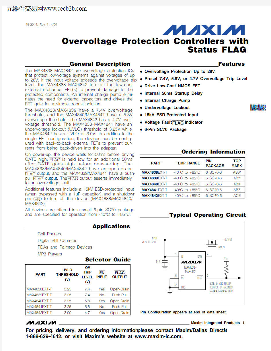
Typical Operating Circuit
19-3044; Rev 1; 4/04
For pricing, delivery, and ordering information,please contact Maxim/Dallas Direct!at 1-888-629-4642, or visit Maxim’s website at https://www.doczj.com/doc/ce3539763.html,.
Pin Configuration appears at end of data sheet.
M A X 4838–M A X 4842
Overvoltage Protection Controllers with Status FLAG 2_______________________________________________________________________________________
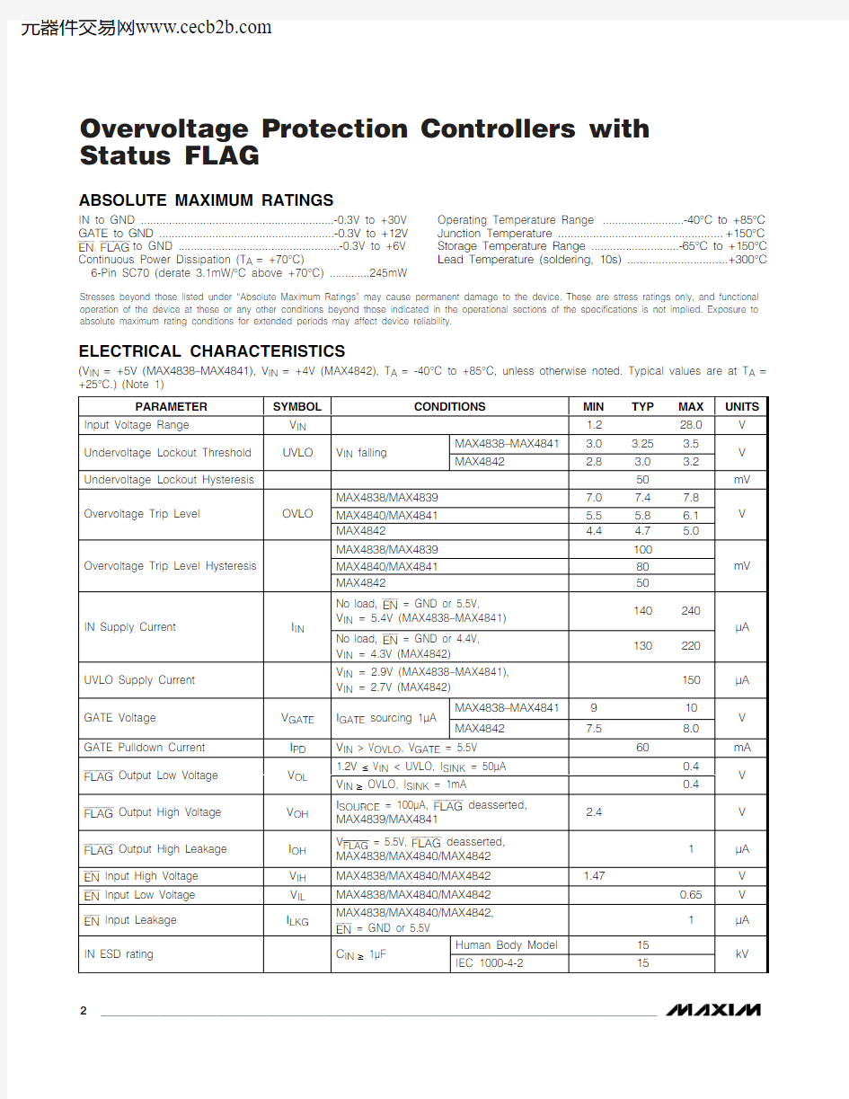
ABSOLUTE MAXIMUM RATINGS
ELECTRICAL CHARACTERISTICS
(V IN = +5V (MAX4838–MAX4841), V IN = +4V (MAX4842), T A = -40°C to +85°C, unless otherwise noted. Typical values are at T A =+25°C.) (Note 1)
Stresses beyond those listed under “Absolute Maximum Ratings” may cause permanent damage to the device. These are stress ratings only, and functional operation of the device at these or any other conditions beyond those indicated in the operational sections of the specifications is not implied. Exposure to absolute maximum rating conditions for extended periods may affect device reliability.
IN to GND ..............................................................-0.3V to +30V GATE to GND ........................................................-0.3V to +12V EN , FLAG to GND ....................................................-0.3V to +6V Continuous Power Dissipation (T A = +70°C)
6-Pin SC70 (derate 3.1mW/°C above +70°C) .............245mW
Operating Temperature Range ..........................-40°C to +85°C Junction Temperature ....................................................+150°C Storage Temperature Range ............................-65°C to +150°C Lead Temperature (soldering, 10s) ................................+300°C
MAX4838–MAX4842
Overvoltage Protection Controllers with
Status FLAG
_______________________________________________________________________________________3
ELECTRICAL CHARACTERISTICS (continued)
(V IN = +5V (MAX4838–MAX4841), V IN = +4V (MAX4842), T A = -40°C to +85°C, unless otherwise noted. Typical values are at T A =+25°C.) (Note 1)
SUPPLY CURRENT vs. INPUT VOLTAGE
M A X 4838 t o c 01
INPUT VOLTAGE (V)
S U P P L Y C U R R E N T (μA )
25
20
15
10
5
10020030040050060000
30
REVERSE CURRENT vs. OUTPUT VOLTAGE
OUTPUT VOLTAGE (V)
R E V E R S E C U R R E N T (μA )
5.04.54.01
10
100
1000
0.1
3.5 5.5
MAX4838–MAX4841
GATE VOLTAGE vs. INPUT VOLTAGE
INPUT VOLTAGE (V)
G A T E V O L T A G E (V )
7
6
5
4
3
6
912
03
8
Typical Operating Characteristics
(V IN = +5V, MAX4838; Si9936DY external MOSFET in back-to-back configuration; T A = +25°C, unless otherwise noted.)
Note 1:All parts are 100% tested at +25°C. Electrical limits across the full temperature range are guaranteed by design and
correlation.
M A X 4838–M A X 4842
Overvoltage Protection Controllers with Status FLAG 4_______________________________________________________________________________________
Typical Operating Characteristics (continued)
(V IN = +5V, MAX4838; Si9936DY external MOSFET in back-to-back configuration; T A = +25°C, unless otherwise noted.)
MAX4842
GATE VOLTAGE vs. INPUT VOLTAGE
INPUT VOLTAGE (V)
G A T E V O L T A G E (V )
7
6
5
1
2
3
4
36
91200
8
GATE VOLTAGE vs. INPUT VOLTAGE
INPUT VOLTAGE (V)
G A T E V O L T A G E (V )
5.4
5.3
5.2
5.1
9.510.0
10.511.0
9.0
5.0
5.5
MAX4838–MAX4841POWER-UP RESPONSE
IN
GATE
5V 0V 0V 5V
0V 5V
10V OUT
FLAG
20ms/div
R OUT = ∞C OUT = 0
MAX4838–MAX4841POWER-UP RESPONSE
20ms/div
5V
0V 0V 1A 0A 5V FLAG I IN GATE
IN
0V
10V R OUT = 5?
OVERVOLTAGE RESPONSE
400ns/div
IN
GATE
I GATE FLAG
5V 8V 0V 40mA
0A 5V 0V
10V POWER-UP OVERVOLTAGE RESPONSE
MAX4838 toc11
1μs/div
8V GATE
IN
I GATE
FLAG
5V
0V 50mA
0A 5V 0V
0V
GATE PULLED UP TO IN WITH 100?
POWER-DOWN RESPONSE
MAX4838 toc12
10ms/div
5V IN
GATE
OUT
FLAG
10V
0V 5V
0V 5V
0V
0V R LOAD = 50?
R FLAG = 100k ? TO +5V
MAX4838 toc08
20ms/div
OUT
GATE
IN
R OUT = ∞C OUT = 0
MAX4838 toc09
FLAG
I GATE
IN
R OUT = 5?
MAX4838–MAX4842
Overvoltage Protection Controllers with
Status FLAG
_______________________________________________________________________________________
5
Figure 1. Startup Timing Diagram
Figure 2. Shutdown Timing Diagram
Figure 3. Power-Up Overvoltage Timing Diagram Figure 4. Disable Timing Diagram
M A X 4838–M A X 4842
Overvoltage Protection Controllers with Status FLAG
Figure 5. Functional Diagram
MAX4838–MAX4842
Overvoltage Protection Controllers with
Status FLAG
_______________________________________________________________________________________7
cally 50ms after the GATE starts going high. At this point the device is in its on state.
At any time if V IN drops below UVLO, FLAG is driven low and GATE is driven to ground.
Applications Information
MOSFET Configuration
The MAX4838–MAX4842 can be used with either a sin-gle MOSFET configuration as shown in the Typical Operating Circuit , or can be configured with a back-to-back MOSFET as shown in Figure 7.
The MAX4838–MAX4842 can drive either a single MOSFET or back-to-back MOSFETs. The back-to-back configuration has almost zero reverse current when the input supply is below the output.
If reverse current leakage is not a concern, a single MOSFET can be used. This approach has half the loss of the back-to-back configuration when used with simi-lar MOSFET types, and is a lower cost solution. Note that if the input is actually pulled low, the output is pulled low as well due to the parasitic body diode in the
MOSFET. If this is a concern, then the back-to-back configuration should be used.
MOSFET Selection
The MAX4838–MAX4842 are designed for use with either a single n-channel MOSFET or dual back-to-back n-channel MOSFETs. In most situations, MOSFETs with R DS(ON) specified for a V GS of 4.5V work well. If the input supply is near the UVLO maximum of 3.5V con-sider using a MOSFET specified for a lower V GS volt-age. Also the V DS should be 30V for the MOSFET to withstand the full 28V IN range of the MAX4838–MAX4842. Table 1 shows a selection of MOSFETs appropriate for use with the MAX4838–MAX4842.
IN Bypass Considerations
For most applications, bypass IN to GND with a 1μF ceramic capacitor. If the power source has significant inductance due to long lead length, take care to pre-vent overshoots due to the LC tank circuit and provide protection if necessary to prevent exceeding the 30V absolute maximum rating on IN.
The MAX4838–MAX4842 provide protection against volt-age faults up to 28V, but this does not include negative voltages. If negative voltages are a concern, connect a Schottky diode from IN to GND to clamp negative input voltages.
ESD Test Conditions
ESD performance depends on a number of conditions.The MAX4838–MAX4842 are specified for 15kV typical ESD resistance on IN when IN is bypassed to ground with a 1μF ceramic capacitor. Contact Maxim for a reli-
Figure 6. State Diagram
Figure 7. Back-to-Back External MOSFET Configuration
M A X 4838–M A X 4842
Overvoltage Protection Controllers with Status FLAG 8_______________________________________________________________________________________
and results.
Human Body Model
Figure 8 shows the Human Body Model and Figure 9shows the current waveform it generates when dis-charged into a low impedance. This model consists of a 100pF capacitor charged to the ESD voltage of inter-est, which is then discharged into the device through a 1.5k ?resistor.
IEC 1000-4-2
Since January 1996, all equipment manufactured and/or sold in the European community has been required to meet the stringent IEC 1000-4-2 specification. The IEC 1000-4-2 standard covers ESD testing and performance of finished equipment; it does not specifically refer to
design equipment that meets Level 3 of IEC 1000-4-2,without additional ESD-protection components.
The main difference between tests done using the Human Body Model and IEC 1000-4-2 is higher peak current in IEC 1000-4-2. Because series resistance is lower in the IEC 1000-4-2 ESD test model (Figure 10),the ESD-withstand voltage measured to this standard is generally lower than that measured using the Human Body Model. Figure 11 shows the current waveform for the ±8kV IEC 1000-4-2 Level 4 ESD Contact Discharge test. The Air-Gap test involves approaching the device with a charger probe. The Contact Discharge method connects the probe to the device before the probe is energized.
Figure 8. Human Body ESD Test Model Figure 9. Human Body Model Current Waveform
MAX4838–MAX4842
Overvoltage Protection Controllers with
Status FLAG
_______________________________________________________________________________________9
Pin Configuration
Chip Information
TRANSISTOR COUNT: 737PROCESS: BiCMOS
M A X 4838–M A X 4842
Overvoltage Protection Controllers with Status FLAG Maxim cannot assume responsibility for use of any circuitry other than circuitry entirely embodied in a Maxim product. No circuit patent licenses are implied. Maxim reserves the right to change the circuitry and specifications without notice at any time.
10____________________Maxim Integrated Products, 120 San Gabriel Drive, Sunnyvale, CA 94086 408-737-7600?2004 Maxim Integrated Products
Printed USA
is a registered trademark of Maxim Integrated Products.
Package Information
(The package drawing(s) in this data sheet may not reflect the most current specifications. For the latest package outline information go to https://www.doczj.com/doc/ce3539763.html,/packages .)