MPEG Clock Generator with VCXO
CY241V08A-11
Features
?Integrated phase-locked loop (PLL)?Low-jitter, high-accuracy outputs ?VCXO with analog adjust
?3.3V operation Benefits
?Highest-performance PLL tailored for multimedia applica-tions
?Meets critical timing requirements in complex system
designs
?Application compatibility for a wide variety of designs
Table 1.Frequency Table
Part Number Outputs Input Frequency Range
Output
Frequencies
VCXO Control
Curve Other Features
CY241V08A-11113.5-MHz pullable crystal input
per Cypress specification One copy of 54 MHz linear Pinout-compatible with
CY2411
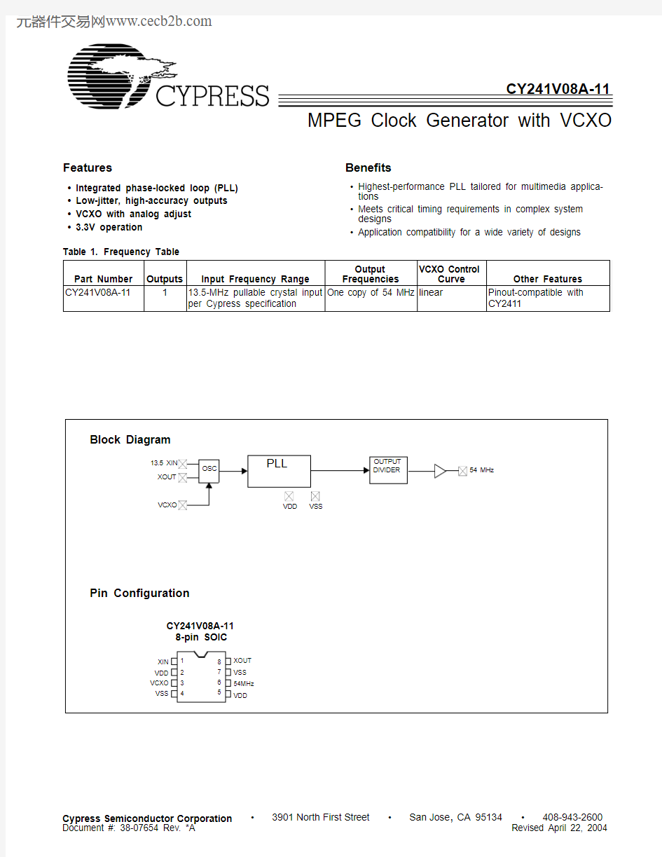
Pin Descriptions
Name Pin Number Description XIN1Reference crystal input.
VDD2,5Voltage supply.
VCXO3Input analog control for VCXO.
VSS4,7Ground.
54MHz654MHz clock output.
XOUT8Reference crystal output.
Absolute Maximum Conditions
Supply Voltage (V DD)........................................–0.5 to +7.0V DC Input Voltage......................................–0.5V to V DD + 0.5 Storage Temperature (Non-condensing).....–55°C to +125°C Junction Temperature................................ –40°C to +125°C Data Retention @ Tj = 125°C................................> 10 years Package Power Dissipation......................................350 mW ESD (Human Body Model) MIL-STD-883.................> 2000V (Above which the useful life may be impaired. For user guide-lines, not tested.)
Pullable Crystal Specifications[1]
Parameter Description Comments Min.Typ.Max.Unit F NOM Nominal crystal frequency Parallel resonance, fundamental mode, AT cut–13.5 –MHz C LNOM Nominal load capacitance–14–pF R1Equivalent series resistance (ESR)Fundamental mode––25?
R3/R1Ratio of third overtone mode ESR to
fundamental mode ESR Ratio used because typical R1 values are much
less than the maximum spec
3–––
DL Crystal drive level No external series resistor assumed150––μW F3SEPHI Third overtone separation from 3*F NOM High side300––ppm F3SEPLO Third overtone separation from 3*F NOM Low side–––150ppm C0Crystal shunt capacitance––7pF C0/C1Ratio of shunt to motional capacitance180–250–C1Crystal motional capacitance14.41821.6fF
Parameter Description Min.Typ.Max.Unit VDD Operating Voltage 3.135 3.3 3.465V T A Ambient Temperature0–70°C C LOAD Max. Load Capacitance ––15pF t PU Power-up time for all V DD pins to reach minimum specified voltage
(power ramps must be monotonic)
0.05–500ms
DC Electrical Specifications
Parameter Name Description Min.Typ.Max.Unit
I OH Output HIGH Current V OH = V DD – 0.5V, V DD = 3.3V1224–mA
I OL Output LOW Current V OL = 0.5V, V DD = 3.3V1224–mA
C IN Input Capacitance Except XIN, XOUT pins––7pF
V VCXO VCXO Input Range0–V DD V
f?XO[2]VCXO Pullability Range Low Side–––115ppm
High Side115––ppm I VDD Supply Current–3035mA AC Electrical Specifications (V DD = 3.3V)[3]
Parameter[3]Name Description Min.Typ.Max.Unit DC Output Duty Cycle Duty Cycle is defined in Figure1, 50% of V DD455055% ER Rising Edge Rate Output Clock Edge Rate, Measured from 20%
to 80% of V DD, C LOAD = 15 pF. See Figure2.
0.8 1.4–V/ns
EF Falling Edge Rate Output Clock Edge Rate, Measured from 80%
to 20% of V DD, C LOAD = 15 pF. See Figure2.
0.8 1.4–V/ns t9Clock Jitter Peak-to-peak period jitter––100ps t10PLL Lock Time––3ms Notes:
1.Crystals that meet this specification include: Ecliptek ECX-5788-13.500M,Siward XTL001050A-13.5-14-400, Raltron A-13.500-14-CL,PDI
HA13500XFSA14XC.
2.–115/+115 ppm assumes 2.5pF of additional board level load capacitance. This range will be shifted down with more board capacitance or shifted up with less
board capacitance.
3.Not 100% tested.
Voltage and Timing Definitions
Test and Measurement Set-up
0.1μF
VDD
Outputs C LOAD
GND
DUT
Ordering Information
Ordering Code Package Name Package Type Operating Range Operating Voltage Features
CY241V08ASC-11S8
8-pin SOIC
Commercial
3.3V Linear VCXO control curve CY241V08ASC-11T
S8
8-pin SOIC – Tape and Reel Commercial
3.3V
Linear VCXO control curve
Figure 1.Duty Cycle Definition
Figure 2.ER = (0.6 x V DD ) /t3, EF = (0.6 x V DD ) /t4
Package Drawing and Dimensions
Document History Page
Document Title: CY241V08A-11 MPEG Clock Generator with VCXO Document Number: 38-07654
REV.ECN NO.Issue
Date
Orig. of
Change Description of Change
**214071See ECN RGL New Data Sheet
*A220461See ECN RGL Minor Change: To post on web