
MOSEL VITELIC V53C516165A
5 VOLT 1M X 1
6 EDO PAGE MODE
CMOS DYNAMIC RAM
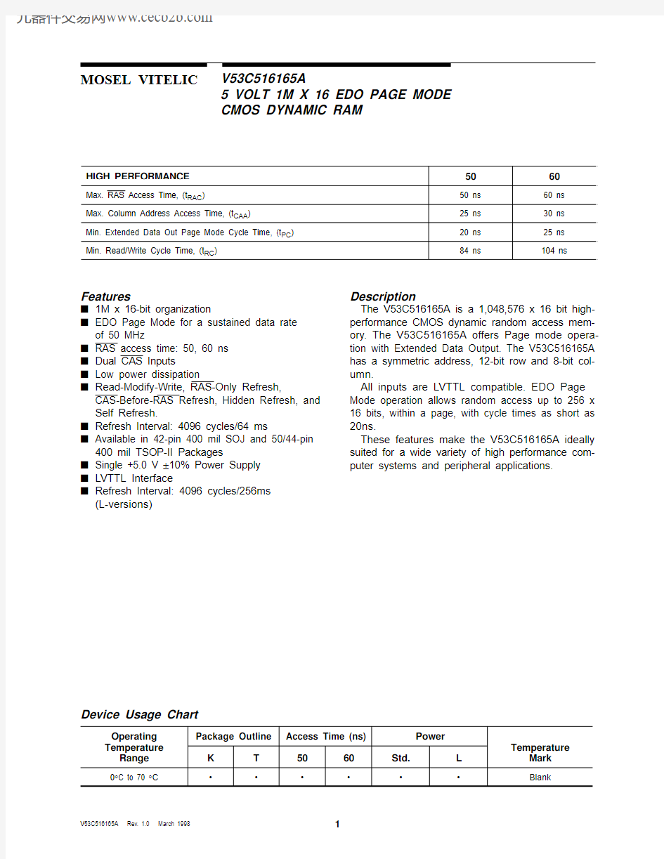
HIGH PERFORMANCE5060 Max. RAS Access Time, (t RAC)50 ns60 ns Max. Column Address Access Time, (t CAA)25 ns30 ns Min. Extended Data Out Page Mode Cycle Time, (t PC)20 ns25 ns Min. Read/Write Cycle Time, (t RC)84 ns104 ns
Features
s1M x 16-bit organization
s EDO Page Mode for a sustained data rate of 50 MHz
s RAS access time: 50, 60 ns
s Dual CAS Inputs
s Low power dissipation
s Read-Modify-Write, RAS-Only Refresh, CAS-Before-RAS Refresh, Hidden Refresh, and Self Refresh.
s Refresh Interval: 4096 cycles/64 ms
s Available in 42-pin 400 mil SOJ and 50/44-pin 400 mil TSOP-II Packages
s Single +5.0 V ±10% Power Supply
s LVTTL Interface
s Refresh Interval: 4096 cycles/256ms
(L-versions)Description
The V53C516165A is a 1,048,576 x 16 bit high-performance CMOS dynamic random access mem-ory. The V53C516165A offers Page mode opera-tion with Extended Data Output. The V53C516165A has a symmetric address, 12-bit row and 8-bit col-umn.
All inputs are LVTTL compatible. EDO Page Mode operation allows random access up to 256 x 16 bits, within a page, with cycle times as short as 20ns.
These features make the V53C516165A ideally suited for a wide variety of high performance com-puter systems and peripheral applications.
Device Usage Chart
Operating Temperature Range Package Outline Access Time (ns)Power
Temperature
Mark K T5060Std.L
0°C to 70 °C??????Blank 元器件交易网https://www.doczj.com/doc/cb1961381.html,
MOSEL VITELIC
V53C516165A
42-Pin Plastic SOJ PIN CONFIGURATION
Top View
50/44-Pin Plastic TSOP-II PIN CONFIGURATION
Top View
Description Pkg.Pin Count
SOJ K 42TSOP-II
T
50/44
Pin Names
A 0 –A 11 Row, Column Address Inputs RAS Row Address Strobe
UCAS Column Address Strobe/Upper Byte Control LCAS Column Address Strobe/Lower Byte Control WE Write Enable OE Output Enable I/O 1 –I/O 16 Data Input, Output V CC +5V Supply V SS
0V Supply NC
No Connect
元器件交易网https://www.doczj.com/doc/cb1961381.html,
MOSEL VITELIC
V53C516165A
Block Diagram
Absolute Maximum Ratings*
Operating temperature range..................0 to 70 ° C Storage temperature range ...............-55 to 150 ° C Soldering temperature..................................260 ° C Soldering time...................................................10 s Input/output voltage....-0.5 to min (V CC +0.5, 7.0) V Power supply voltage ........................-1.0V to 7.0 V Power dissipation ..........................................1.0 W Data out current (short circuit)......................50 mA
* Note: Operation above Absolute Maximum Ratings can
adversely affect device reliability.
Capacitance*
T A = 25 ° C, V CC =5 V ± 10%, V SS = 0 V, f = 1 MHz
* Note: Capacitance is sampled and not 100% tested.
Symbol Parameter Min.Max.Unit C IN1 Address Input —5pF C IN2 RAS, UCAS, LCAS, WE, OE
—7pF C OUT
Data Input/Output
—
7
pF
元器件交易网https://www.doczj.com/doc/cb1961381.html,
MOSEL VITELIC V53C516165A DC and Operating Characteristics (1-2)
T A = 0°C to 70°C, V CC = 5.0 V ± 10%, V SS = 0 V, t T = 2ns, unless otherwise specified.
Symbol Parameter Access
Time
V53C516165A
Unit Test Conditions Notes Min.Typ.Max.
I LI Input Leakage Current
(any input pin)
–1010μA V SS≤ V IN≤ V CC + 0.3V1
I LO Output Leakage Current
(for High-Z State)–1010μA V SS ≤ V OUT≤ V CC + 0.3V
RAS, CAS at V IH
1
I CC1V CC Supply Current,
Operating 50100mA t RC = t RC (min.)2, 3, 4 6090
I CC2V CC Supply Current,
TTL Standby 2mA RAS, CAS at V IH
other inputs ≥ V SS
I CC3V CC Supply Current,
RAS-Only Refresh 50100mA t RC = t RC (min.)2, 4 6090
I CC4V CC Supply Current,
EDO Page Mode
Operation 5070mA Minimum Cycle2, 3, 4 6055
I CC5V CC Supply Current,
CMOS Standby 1.0mA RAS ≥ V CC – 0.2 V,
CAS ≥ V CC – 0.2 V
1
I CC6Average Self Refresh Current
CBR cycle with t RAS > t RASS min.,
CAS held low, WE = V CC – 0.2V,
Address and D IN = V CC – 0.2V
or 0.2V 1.0
250
mA
μA L Version
I CC7V CC Supply Current,
during CAS-before-RAS Refresh 50100mA t RC = t RC (min)2, 4 6090
V IL Input Low Voltage –0.50.8V1
V IH Input High Voltage2V CC+0.5V1
V OL Output Low Voltage0.4V I OUT = 4.2 mA1
V OH Output High Voltage 2.4V I OUT = –5 mA1元器件交易网https://www.doczj.com/doc/cb1961381.html,
MOSEL VITELIC V53C516165A AC Characteristics
T A = 0°C to 70°C, V CC =5.0 V ±10%, V SS = 0V, t T = 2ns unless otherwise noted
JEDEC
Symbol Symbol Parameter
5060
Unit Notes Min.Max.Min.Max.
t RL1RH1t RAS RAS Pulse Width5010K6010K ns
t RL2RL2t RC Read or Write Cycle Time84104ns
t RH2RL2t RP RAS Precharge Time3040ns
t RL1CH1t CSH CAS Hold Time4050ns
t CL1CH1t CAS CAS Pulse Width810K1010K ns
t RL1CL1t RCD RAS to CAS Delay12371445ns
t WH2CL2t RCS Read Command Setup Time00ns
t AVRL2t ASR Row Address Setup Time00ns
t RL1AX t RAH Row Address Hold Time810ns
t AVCL2t ASC Column Address Setup Time00ns
t CL1AX t CAH Column Address Hold Time810ns
t CL1RH1(R)t RSH RAS Hold Time1315ns
t CH2RL2t CRP CAS to RAS Precharge Time55ns
t CH2WX t RCH Read Command Hold Time
Referenced to CAS
0 0ns9
t RH2WX t RRH Read Command Hold Time
Referenced to RAS
0 0ns9
t CL1t COH Output Hold after CAS LOW55ns
t GL1QV t OAC Access Time from OE1315ns
t CL1QV t CAC Access Time from CAS1315ns7, 12
t RL1QV t RAC Access Time from RAS5060ns7, 12
t AVQV t CAA Access Time from Column Address2530ns7, 13
t CL1QX t CLZ CAS to Low-Z Output00ns7
t CH2QX t OFF Output Buffer Turnoff Delay013015ns
t CL1QZ t DZC Data to CAS Low Delay00ns15
t RL1AV t RAD RAS to Column Address Delay Time10251230ns
t GL2QZ t OEZ Output Buffer Turnoff Delay from OE013015ns8
t WL1CH1t CWL Write Command to CAS Lead Time1315ns
t WL1CL2t WCS Write Command Setup Time00ns11
t CL1WH1t WCH Write Command Hold Time810ns
t WL1WH1t WP Write Pulse Width810ns
t GL1QZ t DEO Data to OE Delay00ns15
t WL1RH1t RWL Write Command to RAS Lead Time1315ns
t DVWL2t DS Data in Setup Time00ns10元器件交易网https://www.doczj.com/doc/cb1961381.html,
t WL1DX t DH Data in Hold Time 810ns 10t WL1GL2t WOH Write to OE Hold Time
1013ns 10
t CH2RH2t PRWC EDO Page Mode Read-Write Cycle Time 5868ns t RL2RL2(RMW)t RWC Read-Modify-Write Cycle Time 113138ns t CL1WL2t CWD CAS to WE Delay
2732ns 10t RL1WL2t RWD RAS to WE Delay in Read-Modify-Write Cycle 6477ns 10t AVWL2t AWD Column Address to WE Delay
3947ns 10
t CL2CL2t PC EDO Page Mode Read or Write Cycle Time 2025ns t CH2CL2t CP CAS Precharge Time
810ns t AVRH1t CAR Column Address to RAS Setup Time 25
30
ns t CH2QV t CAP Access Time from Column Precharge 27
32
ns 6
t CL1RL2t CSR CAS Setup Time CAS-before-RAS Refresh
1010ns t RH2CL2t RPC RAS to CAS Precharge Time
55ns t RL1CH1t CHR CAS Hold Time CAS-before-RAS Refresh 1010ns t RH2CL2t RASP RAS Pulse Width (EDO Mode)50200K
60200K ns t RH2CL2t RHCP CAS Precharge Time to RAS Delay 2732ns t RH2CL2t CPWD CAS Precharge Time to WE
4149ns t RH2CL2t CPT CAS Precharge Time (CBR Counter Test)3540ns t RH2CL2t WRP Write to RAS Precharge time (CRB Cycle)1010ns t RH2CL2t WRH Write Hold time reference to RAS (CRB Cycle)
1010ns t RH2CL2t CDD CAS High to Data delay 1013ns 16t RH2CL2t ODD OE High to Data delay 1013ns 16
t T
t T Transition Time (Rise and Fall)1
501
50ns t REF
Refresh Interval (4096 Cycles)
6464ms
Self Refresh AC Characteristics
t RASS RAS Pulse Width During Self Refresh 100K 100K ns 17t RPS RAS Precharge Time During Self Refresh 95110ns 17t CHS CAS Hold Time Width During Self Rerfresh 50
50
ns 17
t REF
Refresh period for L-Version
256
256
ms
JEDEC
Symbol Symbol
Parameter
50
60Unit
Notes
Min.
Max.Min.
Max.AC Characteristics (Cont’d)
Notes:
1. All voltage are referenced to V SS.
2.I CC1, I CC3, I CC4, and I CC7 depend on cycle rate.
3.I CC1 and I CC4 depend on output loading. Specified values are measured with the output open.
4.Address can be changed once or less while RAS = V IL. In the case of I CC4 it can be changed once or less during
an EDO cycle (t HPC).
5.An initial pause of 200 μs is required after power-up followed by 8 RAS cycles of which at least one cycle has to be
a refresh cycle, before proper device operation is achieved. In case of using internal refresh counter, a minimum of
8 CAS-before-RAS initialization cycles instead of 8 RAS cycles are required.
6.V IH (min.) and V IL (max.) are reference levels for measuring timing of input signals. Transition times are also mea-
sured between V IH and V IL.
7.Measured with a load equivalent to 2 TTL gates and 50 pF (V OL = 0.8V and V OH = 2.0V).
8.t OFF (max.) and t OEZ (max.) define the time at which the outputs acheive the open-circuit condition and are not ref-
erenced to output voltage levels.
9.Either t RCH or t RRH must be satisfied for a read cycle.
10.These parameters are referenced to the CAS leading edge in early write cycles and to the WE leading edge in
read-write cycles.
11.t WCS, t RWD, t CWD, t AWD and t CPWD are not restrictive operating parameters. They are included in the data sheet as
electrical characteristics only. If t WCS > t WCS (min.), the cycle is an early write cycle and the I/O pin will remain open-circuit (high impedance) through the entire cycle; if t RWD > t RWD (min.), t CWD > t CWD (min.), t AWD > t AWD (min.), and t CPWD > t CPWD (min.), the cycle is a read-write cycle and I/O pins will contain data read from the selected cells. If neither of the above sets of conditions is satisfied, the condition of the I/O pins (at access time) is indeterminate.
12.Operation within the t RCD (max.) limit ensures that t RAC (max.) can be met. t RCD (max.) is specified as a reference
point only: if t RCD is greater than the specified t RCD (max.) limit, then access time is controlled by t CAC.
13.Operation within the t RAD (max) limit ensures that t RAC (max.) can be met. t RAD (max.) is specified as a reference
point only: if t RAD is greater than the specified t RAD (max.) limit, then access time is controlled by t CAA.
14.AC measurements assume t T = 2 ns.
15.Either t DZC or t DEO must be satisfied.
16.Either t CDD or t ODD must be satisfied.
17.When using Self Refresh mode, the following refresh operations must be performed to ensure proper DRAM oper-
ation:
If row addresses are being refreshed on an evenly distributed manner over the refresh interval using CBR refresh cycles, then only one CBR cycle must be performed immediately after exit from Self Refresh.
If row addresses are being refreshed in any other manner (ROR – Distributed/Burst; or CBR – Burst) over the re-fresh interval, then a full set of row refreshes must be performed immediately before entry to and immediately after exit from Self Refresh.
18.t OFF is referenced from the rising edge of RAS or CAS, whichever occurs last.
Waveforms of Read Cycle
RAS
UCAS
Address
WE
OE
I/O
(Inputs)
I/O
(Outputs)
V IH
V IL
“H” or “L”
511816502-04
V IH V IL
V IH
V IL
V IH
V IL
V IH
V IL
V IH V IL
V V LCAS
Waveforms of Write Cycle (Early Write) RAS
Address
WE
OE
I/O
(Inputs)
I/O (Outputs)
“H” or “L”
511816502-05 V IH
V IL
V IH
V IL
V IH
V IL
V IH
V IL
V IH
V IL
V IH
V IL
V OH
V OL
UCAS LCAS
Waveforms of Write Cycle (OE Controlled Write)
“H” or “L”
RAS
Address
WE
OE
I/O
(Inputs)
I/O
(Outputs)
511816502-06
V IH
V IL
V V V IH V IL
V IH
V IL
V IH
V IL
V IH
V IL
V IH V IL
UCAS
LCAS
Waveforms of Read-Write (Read-Modify-Write) Cycle
I/O
(Outputs)
I/O
(Inputs)
OE
WE
“H” or “L”
RAS
Address
511816502-07
V IH V IL
V IH V IL
V IH
V IL
V IH
V IL
V IH
V IL
V IH
V IL
V OL
V UCAS LCAS
Waveforms of EDO Page Mode Read Cycle
RAS
I/O WE
Address
V IH
V IL
“H” or “L”
OE
(Output)
511816502-08
V IH V IL
V IH
V IL
V IH
V IL
V OH
V OL
V IH V IL
UCAS LCAS
Waveforms of EDO Page Mode Read Cycle (OE Control)
RAS
I/O WE
Address
“H” or “L”
OE
(Output)
511816502-09
V IH
V IL
V IH
V IL
V IH
V IL
V IH
V IL
V V V IH V IL
UCAS LCAS
Waveforms of EDO Page Mode Read Cycle (WE Control)
RAS
I/O WE
Address
“H” or “L”
OE
(Output)
511816502-10
V IH
V IL
V IH V IL
V IH
V IL
V IH
V IL
V V V IH V IL
UCAS LCAS
Waveforms of EDO Page Mode Early Write Cycle
RAS
I/O (Input)
WE
Address
“H” or “L”
OE
511816502-11
V IH
V IL
V IH V IL
V IH
V IL
V IH
V IL
V V V IH
V IL
UCAS LCAS
Waveforms of EDO Page Mode Late Write Cycle
RAS
I/O WE
Address
“H” or “L”
OE
(Input)
511816502-12
V IH
V IL
V IH V IL
V IH
V IL
V IH
V IL
V V V IH V IL
UCAS LCAS
Waveforms of EDO Page Mode Read-Modify-Write Cycle
R A S W E
O E
A d d r e s s
I /O (I n p u t s )
I /O (O u t p u t s )
V I V I V I V I V I V I V I V I V I V I V I V I V O V O U C A S L C A S
511816502-13
Waveforms of RAS Only Refresh Cycle
Address
RAS
I/O
(Outputs)
“H” or “L”
V IH V IL
V IH V IL
V IH
V IL
V OH
V OL
UCAS LCAS
511816502-14
Waveforms of CAS-before-RAS Refresh Cycle
“H” or “L”
RAS
I/O
(Outputs)I/O
(Inputs)
OE
WE
V V IL
V V IL
V V IL
V V IL
V V IL
V V UCAS LCAS
511816502-15
Waveforms of CAS-before-RAS Self Refresh Cycle (Optional)
“H” or “L”
RAS
I/O
(Outputs)I/O
(Inputs)
OE
WE
V V IL
V V IL
V V IL
V V IL
V V IL
V V UCAS LCAS
511816502-15