
R a d i a t e d E M I E m i s s i o n s (d B μV /m )
Frequency (MHz)
C001
Product Folder
Sample &Buy
Technical Documents Tools &Software
Support &Community
LM43602
ZHCSCC9A –APRIL 2014–REVISED APRIL 2014
LM43602SIMPLE SWITCHER?3.5V 至36V 2A 同步降压电压转换器
1特性
3说明
?稳压静态电流27μA
LM43602SIMPLE SWITCHER ?稳压器是一款易于使用的同步降压直流到直流转换器,此转换器能够驱动高?
轻负载时的高效率(断续传导模式(DCM)和脉冲频率调制(PFM))
达2A 的负载电流(输入电压范围为3.5V 至36V (最?符合EN55022/CISPR 22电磁干扰(EMI)标准大绝对值42V ))。LM43602在极小解决方案尺寸内?集成同步整流
提供出色的效率、输出精度和压降电压。扩展系列产?可调频率范围:200kHz 至2.2MHz (缺省值品能够以引脚到引脚兼容封装提供0.5A ,1A 和3A 负500kHz )
载电流选项。采用峰值电流模式控制来实现简单控制?与外部时钟频率同步环路补偿和逐周期电流限制。其他诸如可编程开关频?内部补偿1
率、同步、电源正常标志、精确使能、内部软启动、可?与几乎任一陶瓷、固态电解、钽和铝质电容器组合扩展软启动和跟踪等特性可以为广泛应用提供灵活且易一同工作时保持稳定于使用的平台。轻负载时的断续传导和自动频率调制?电源正常标志
可提升轻负载效率。此系列只需要很少的外部组件,?软启动进入预偏置负载并且引脚排列可实现简单、最优的印刷电路板(PCB)?内部软启动:4.1ms
布局布线。保护特性包括热关断,V CC 欠压闭锁,逐?可由外部电容器延长的软启动时间周期电流限制和输出短路保护。LM43602器件采用带?输出电压跟踪功能
散热片薄型小外形尺寸(HTSSOP)/PWP 16引线封装?程序系统欠压闭锁(UVLO)精确使能(5.1mm x 6.6mm x 1.2mm)。
?具有断续模式的输出短路保护器件信息
?
过热热关断保护
订货编号
封装
封装尺寸LM43602PWP
HTSSOP (16)
5.1mm x
6.6mm
2应用范围
?工业用电源?电信系统
?AM 以下波段汽车应用?通用宽V IN 稳压?
高效负载点稳压
4简化电路原理图
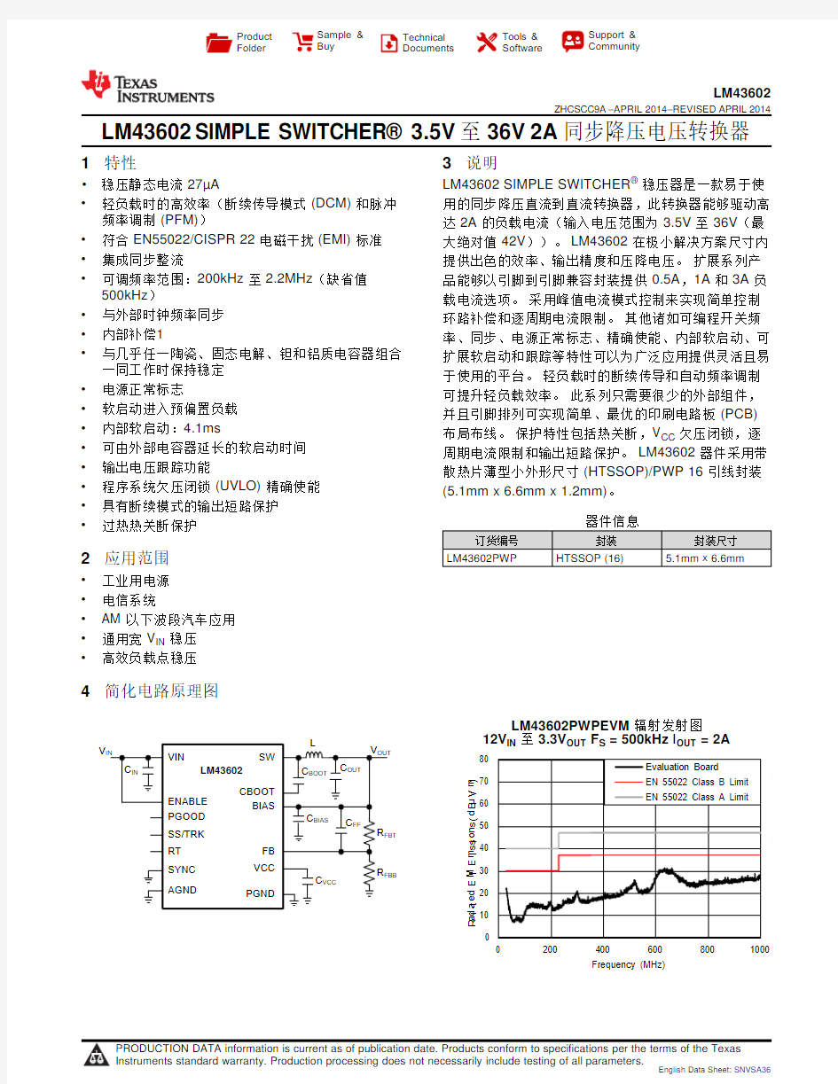
LM43602PWPEVM 辐射发射图
12V IN 至3.3V OUT F S =500kHz I OUT =2A
LM43602
ZHCSCC9A–APRIL2014–REVISED https://www.doczj.com/doc/b518642439.html,
目录
8.1Overview (12)
1特性 (1)
8.2Functional Block Diagram (12)
2应用范围 (1)
8.3Feature Description (13)
3说明 (1)
8.4Device Functional Modes (20)
4简化电路原理图 (1)
9Applications and Implementation (22)
5修订历史记录 (2)
9.1Application Information (22)
6Pin Configuration and Functions (3)
9.2Typical Applications (22)
7Specifications (4)
10Power Supply Recommendations (33)
7.1Absolute Maximum Ratings (4)
11Layout (33)
7.2Handling Ratings (4)
11.1Layout Guidelines (33)
7.3Recommended Operating Conditions (4)
11.2Layout Example (36)
7.4Thermal Information (5)
12器件和文档支持 (37)
7.5Electrical Characteristics (5)
12.1Trademarks (37)
7.6Timing Requirements (6)
12.2Electrostatic Discharge Caution (37)
7.7Switching Characteristics (7)
12.3Glossary (37)
7.8Typical Characteristics (7)
13机械封装和可订购信息 (37)
8Detailed Description (12)
5修订历史记录
Changes from Original(April2014)to Revision A Page ?已更改器件从产品预览改为生产数据 (1)
SW VIN PGND CBOOT VCC BIAS SYNC RT PGOOD
EN SS/TRK AGND FB
SW PGND
VIN LM43602
https://www.doczj.com/doc/b518642439.html,
ZHCSCC9A –APRIL 2014–REVISED APRIL 2014
6Pin Configuration and Functions
16-Pin HTSSOP (PWP)
Top View
Pin Functions
PIN
DESCRIPTION
NAME NUMBER SW 1,2Switching output of the regulator.Internally connected to both power MOSFETs.Connect to power inductor.
CBOOT 3Boot-strap capacitor connection for high-side driver.Connect a high quality 470nF capacitor from CBOOT to SW.
VCC
4
Internal bias supply output for bypassing.Connect bypass capacitor from this pin to
AGND.Do not connect external loading to this pin.Never short this pin to ground during operation.
BIAS 5
Optional internal LDO supply input.To improve efficiency,it is recommended to tie to V OUT when 3.3V ≤V OUT ≤28V,or tie to an external 3.3V or 5V rail if available.When used,place a bypass capacitor (1to 10μF)from this pin to ground.Tie to ground when not in use.
SYNC 6Clock input to synchronize switching action to an external https://www.doczj.com/doc/b518642439.html,e proper high speed termination to prevent ringing.Connect to ground if not used.
RT 7Connect a resistor R T from this pin to AGND to program switching frequency.Leave floating for 500kHz default switching frequency.
PGOOD 8Open drain output for power-good https://www.doczj.com/doc/b518642439.html,e a 10k Ωto 100k Ωpull-up resistor to logic rail or other DC voltage no higher than 12V.
FB 9Feedback sense input pin.Connect to the midpoint of feedback divider to set V OUT .Do not short this pin to ground during operation.
AGND 10Analog ground pin.Ground reference for internal references and logic.Connect to system ground.
SS/TRK 11Soft-start control pin.Leave floating for internal soft-start slew rate.Connect to a capacitor to extend soft start time.Connect to external voltage ramp for tracking.EN
12
Enable input to the internal LDO and regulator.High =ON and low =OFF.Connect to VIN,or to VIN through resistor divider,or to an external voltage or logic source.Do not float.
VIN 13,14
Supply input pins to internal LDO and high side power FET.Connect to power supply and bypass capacitors C IN .Path from VIN pin to high frequency bypass C IN and PGND must be as short as possible.
PGND 15,16
Power ground pins,connected internally to the low side power FET.Connect to system ground,PAD,AGND,ground pins of C IN and C OUT .Path to C IN must be as short as possible.
PAD 17
Low impedance connection to AGND.Connect to PGND on PCB.Major heat dissipation path of the die.Must be used for heat sinking to ground plane on PCB.
LM43602
ZHCSCC9A–APRIL2014–REVISED https://www.doczj.com/doc/b518642439.html, 7Specifications
7.1Absolute Maximum Ratings(1)
Over operating free-air temperature range(unless otherwise noted)
PARAMETER MIN MAX UNIT Input Voltages VIN to PGND-0.342(2)V
EN to PGND-0.3VIN+0.3
FB,RT,SS/TRK to AGND-0.3 3.6
PGOOD to AGND-0.315
SYNC to AGND-0.3 5.5
BIAS to AGND-0.330
AGND to PGND-0.30.3
Output Voltages SW to PGND-0.3VIN+0.3V
SW to PGND less than10ns Transients-3.542
CBOOT to SW-0.3 5.5
VCC to AGND-0.3 3.6
Operating Junction Temperature T J-40+125°C
(1)Stresses beyond those listed under Absolute Maximum Ratings may cause permanent damage to the device.These are stress ratings
only,and functional operation of the device at these or any other conditions beyond those indicated under Recommended Operating Conditions is not implied.Exposure to absolute-maximum-rated conditions for extended periods may affect device reliability.
(2)At max duty cycle of0.01%
7.2Handling Ratings
PARAMETER DEFINITION MIN MAX UNIT
T stg Storage temperature range-65+150°C
V ESD(1)(2)HBM Human body model 1.0kV
CDM Charge device model0.5
(1)Electrostatic discharge(ESD)to measure device sensitivity/immunity to damage caused by assembly line electrostatic discharges into
the device.
(2)ESD testing is performed according to the respective JESD22JEDEC standard.
7.3Recommended Operating Conditions(1)
Over operating free-air temperature range(unless otherwise noted)
PARAMETER MIN MAX UNIT Input Voltages VIN to PGND 3.536V EN-0.3VIN
FB-0.3 1.1
PGOOD-0.312
BIAS input not used-0.30.3
BIAS input used 3.328
AGND to PGND-0.10.1
Output Voltage V OUT 1.028V Output Current I OUT02A Temperature Operating junction temperature range,T J-40+125°C (1)Operating Ratings indicate conditions for which the device is intended to be functional,but do not guarantee specific performance limits.
For guaranteed specifications,see Electrical Characteristics.
LM43602 https://www.doczj.com/doc/b518642439.html, ZHCSCC9A–APRIL2014–REVISED APRIL2014
7.4Thermal Information
HTSSOP
THERMAL METRIC(1)(2)UNIT
(16PINS)
RθJA Junction-to-ambient thermal resistance38.9(3)
RθJC(top)Junction-to-case(top)thermal resistance24.3
RθJB Junction-to-board thermal resistance19.9
°C/W
ψJT Junction-to-top characterization parameter0.7
ψJB Junction-to-board characterization parameter19.7
RθJC(bot)Junction-to-case(bottom)thermal resistance 1.7
(1)The package thermal impedance is calculated in accordance with JESD51-7;
(2)Thermal Resistances were simulated on a4layer,JEDEC board.
(3)See Figure64forθJA vs Copper Area Curve
7.5Electrical Characteristics
Limits apply over the recommended operating junction temperature(T J)range of-40°C to+125°C,unless otherwise stated. Minimum and Maximum limits are specified through test,design or statistical correlation.Typical values represent the most likely parametric norm at T J=25°C,and are provided for reference purposes only.Unless otherwise stated,the following conditions apply:V IN=12V,V OUT=3.3V,F S=500kHz.
SYMBOL PARAMETER CONDITIONS MIN TYP MAX UNIT SUPPLY VOLTAGE(VIN PIN)
V IN-MIN-ST Minimum input voltage for startup 3.8V
I SHDN Shutdown quiescent current V EN=0V 1.2 3.1μA
I Q-NONSW V EN=3.3V
Operating quiescent current(non-
V FB=1.5V 5.010μA switching)from V IN
V BIAS=3.4V external
I BIAS-NONSW V EN=3.3V
Operating quiescent current(non-
V FB=1.5V85130μA switching)from external V BIAS
V BIAS=3.4V external
I Q-SW V EN=3.3V
I OUT=0A
Operating quiescent current(switching)R T=open27μA
V BIAS=V OUT=3.3V
R FBT=1.0Meg
ENABLE(EN PIN)
V EN-VCC-H Voltage level to enable the internal LDO
V ENABLE high level 1.2V output V CC
V EN-VCC-L Voltage level to disable the internal LDO
V ENABLE low level0.525V output V CC
V EN-VOUT-H Precision enable level for switching and
V ENABLE high level 2.00 2.2 2.42V regulator output:V OUT
V EN-VOUT-HYS Hysteresis voltage between V OUT
V ENABLE hysteresis-290mV precision enable and disable thresholds
I LKG-EN Enable input leakage current V EN=3.3V0.85 1.75μA INTERNAL LDO(VCC and BIAS PINS)
V CC Internal LDO output voltage V CC V IN≥3.8V 3.28V
V CC-UVLO Under voltage lock out(UVLO)V CC rising threshold 3.1V thresholds for V CC Hysteresis voltage between rising and-520mV
falling thresholds
V BIAS-ON Internal LDO input change over V BIAS rising threshold 2.94 3.15V threshold to BIAS Hysteresis voltage between rising and-75mV
falling thresholds
LM43602
ZHCSCC9A–APRIL2014–REVISED https://www.doczj.com/doc/b518642439.html,
Electrical Characteristics(continued)
Limits apply over the recommended operating junction temperature(T J)range of-40°C to+125°C,unless otherwise stated. Minimum and Maximum limits are specified through test,design or statistical correlation.Typical values represent the most likely parametric norm at T J=25°C,and are provided for reference purposes only.Unless otherwise stated,the following conditions apply:V IN=12V,V OUT=3.3V,F S=500kHz.
SYMBOL PARAMETER CONDITIONS MIN TYP MAX UNIT VOLTAGE REFERENCE(FB PIN)
V FB Feedback voltage T J=25oC 1.004 1.011 1.018V
T J=-40oC to85oC0.994 1.011 1.026
T J=-40oC to125oC0.994 1.011 1.030
I LKG-FB Input leakage current at FB pin FB=1.0V0.265nA THERMAL SHUTDOWN
T SD(1)Thermal shutdown Shutdown threshold160oC
Recovery threshold150oC CURRENT LIMIT AND HICCUP
I HS-LIMIT Peak inductor current limit 3.65 4.5 5.15A
I LS-LIMIT Inductor current valley limit 1.75 2.0 2.25A SOFT START(SS/TRK PIN)
I SSC Soft-start charge current 1.25 2.0 2.75μA
R SSD Soft-start discharge resistance UVLO,TSD,OCP,or EN=0V18kΩPOWER GOOD(PGOOD PIN)
V PGOOD-HIGH Power-good flag over voltage tripping%of FB voltage110%113% threshold
V PGOOD-LOW Power-good flag under voltage tripping%of FB voltage77%88%
threshold
V PGOOD-HYS Power-good flag recovery hysteresis%of FB voltage6%
R PGOOD PGOOD pin pull down resistance when V EN=3.3V40125Ωpower bad V
=0V60150
EN
MOSFETS(2)
R DS-ON-HS High-side MOSFET ON-resistance I OUT=1A120mΩ
V BIAS=V OUT=3.3V
R DS-ON-LS Low-side MOSFET ON-resistance I OUT=1A65mΩ
V BIAS=V OUT=3.3V
(1)Guaranteed by design
(2)Measured at the pins
7.6Timing Requirements
MIN TYP MAX UNIT CURRENT LIMIT AND HICCUP
N OC Hiccup wait cycles when LS current limit tripped32Cycles
T OC Hiccup retry delay time 5.5ms SOFT START(SS/TRK PIN)
T SS Internal soft-start time when SS pin open circuit 4.1ms POWER GOOD(PGOOD PIN)
T PGOOD-RISE Power-good flag rising transition deglitch delay220μs
T PGOOD-FALL Power-good flag falling transition deglitch delay220μs
LM43602 https://www.doczj.com/doc/b518642439.html, ZHCSCC9A–APRIL2014–REVISED APRIL2014
7.7Switching Characteristics
over operating free-air temperature range(unless otherwise noted)
PARAMETER TEST CONDITIONS MIN TYP MAX UNIT SW(SW PIN)
Minimum high side MOSFET ON
t ON-MIN(1)125165ns time
Minimum high side MOSFET OFF
t OFF-MIN(1)200250ns time
OSCILLATOR(SW and SYNC PINS)
F OSC-
Oscillator default frequency RT pin open circuit425500580kHz DEFAULT
Minimum adjustable frequency200kHz
F ADJ Maximum adjustable frequency With1%resistors at RT pin2200kHz
Frequency adjust accuracy10%
V SYNC-HIGH Sync clock high level threshold2V
V SYNC-LOW Sync clock low level threshold0.4V
D SYNC-MAX Sync clock maximum duty cycle90%
D SYNC-MIN Sync clock minimum duty cycle10%
Mininum sync clock ON and OFF
T SYNC-MIN80ns time
(1)Guaranteed by design
7.8Typical Characteristics
Unless otherwise specified,V IN=12V,V OUT=3.3V,F S=500kHz,L=6.8μH,C OUT=120μF,C FF=100pF.Please refer to Application Performance Curves for Bill of materials for other V OUT and F S combinations.
LM43602
ZHCSCC9A–APRIL2014–REVISED https://www.doczj.com/doc/b518642439.html,
Typical Characteristics(continued)
Unless otherwise specified,V IN=12V,V OUT=3.3V,F S=500kHz,L=6.8μH,C OUT=120μF,C FF=100pF.Please refer to
LM43602 https://www.doczj.com/doc/b518642439.html, ZHCSCC9A–APRIL2014–REVISED APRIL2014
Typical Characteristics(continued)
Unless otherwise specified,V IN=12V,V OUT=3.3V,F S=500kHz,L=6.8μH,C OUT=120μF,C FF=100pF.Please refer to
CBOOT
VIN BIAS
PGOOD
ENABLE
AGND
PGND
SYNC VCC
SW
FB
RT SS/TRK
LM43602
ZHCSCC9A –APRIL 2014–REVISED APRIL 2014
https://www.doczj.com/doc/b518642439.html,
8Detailed Description
8.1Overview
The LM43602Simple Switcher?regulator is an easy to use synchronous step-down DC-DC converter that operates from 3.5V to 36V supply voltage.It is capable of delivering up to 2A DC load current with exceptional efficiency and thermal performance in a very small solution size.An extended family is available in 0.5A,1A,and 3A load options in pin to pin compatible packages.
The LM43602employs fixed frequency peak current mode control with Discontinuous Conduction Mode (DCM)and Pulse Frequency Modulation (PFM)mode at light load to achieve high efficiency across the load range.The device is internally compensated,which reduces design time,and requires fewer external components.The switching frequency is programmable from 200kHz to 2.2MHz by an external resistor R T .It is default at 500kHz without R T resistor.The LM43602is also capable of synchronization to an external clock within the 200kHz to 2.2MHz frequency range.The wide switching frequency range allows the device to be optimized to fit small board space at higher frequency,or high efficient power conversion at lower frequency.
Optional features are included for more comprehensive system requirements,including power-good (PGOOD)flag,precision enable,synchronization to external clock,extendable soft-start time,and output voltage tracking.These features provide a flexible and easy to use platform for a wide range of applications.Protection features include over temperature shutdown,V CC under-voltage lockout (UVLO),cycle-by-cycle current limit,and short-circuit protection with hiccup mode.
The family requires few external components and the pin arrangement was designed for simple,optimum PCB layout.The LM43602device is available in the HTSSOP /PWP 16pins leaded package.
8.2Functional Block Diagram
V -V I n d u c t o r C u r r e n t
S W V o l t a g e
I I LM43602
https://www.doczj.com/doc/b518642439.html,
ZHCSCC9A –APRIL 2014–REVISED APRIL 2014
8.3Feature Description
8.3.1Fixed Frequency Peak Current Mode Controlled Step-Down Regulator
The following operating description of the LM43602will refer to the Functional Block Diagram and to the waveforms in Figure 25.The LM43602is a step-down Buck regulator with both high-side (HS)switch and low-side (LS)switch (synchronous rectifier)integrated.The LM43602supplies a regulated output voltage by turning on the HS and LS NMOS switches with controlled ON time.During the HS switch ON time,the SW pin voltage V SW swings up to approximately V IN ,and the inductor current i L increases with a linear slope (V IN -V OUT )/L.When the HS switch is turned off by the control logic,the LS switch is turned on after a anti-shoot-through dead time.Inductor current discharges through the LS switch with a slope of -V OUT /L.The control parameter of Buck converters are defined as Duty Cycle D =t ON /T SW ,where t ON is the HS switch ON time and T SW is the switching period.The regulator control loop maintains a constant output voltage by adjusting the duty cycle D.In an ideal Buck converter,where losses are ignored,D is proportional to the output voltage and inversely proportional to the input voltage:D =V OUT /V IN .
Figure 25.SW Node and Inductor Current Waveforms in Continuous Conduction Mode (CCM)The LM43602synchronous Buck converter employs peak current mode control topology.A voltage feedback loop is used to get accurate DC voltage regulation by adjusting the peak current command based on voltage offset.The peak inductor current is sensed from the HS switch and compared to the peak current to control the ON time of the HS switch.The voltage feedback loop is internally compensated,which allows for fewer external components,makes it easy to design,and provides stable operation with almost any combination of output capacitors.The regulator operates with fixed switching frequency in Continuous Conduction Mode (CCM)and Discontinuous Conduction Mode (DCM).At very light load,the LM43602will operate in PFM to maintain high efficiency and the switching frequency will decrease with reduced load current.8.3.2Light Load Operation
DCM operation is employed in the LM43602when the inductor current valley reaches zero.The LM43602will be in DCM when load current is less than half of the peak-to-peak inductor current ripple in CCM.In DCM,the LS switch is turned off when the inductor current reaches zero.Switching loss is reduced by turning off the LS FET at zero current and the conduction loss is lowered by not allowing negative current conduction.Power conversion efficiency is higher in DCM than CCM under the same conditions.
In DCM,the HS switch ON time will reduce with lower load current.When either the minimum HS switch ON time (t ON-MIN )or the minimum peak inductor current (I PEAK-MIN )is reached,the switching frequency will decrease to maintain regulation.At this point,the LM43602operates in PFM.In PFM,switching frequency is decreased by the control loop when load current reduces to maintain output voltage regulation.Switching loss is further reduced in PFM operation due to less frequent switching actions.
FB
FBB FBT
OUT FB V R R V V
LM43602
ZHCSCC9A –APRIL 2014–REVISED APRIL 2014
https://www.doczj.com/doc/b518642439.html,
Feature Description (continued)
In PFM operation,a small positive DC offset is required at the output voltage to activate the PFM detector.The lower the frequency in PFM,the more DC offset is needed at V OUT .Please refer to the Typical Characteristics for typical DC offset at very light load.If the DC offset on V OUT is not acceptable for a given application,a static load at output is recommended to reduce or eliminate the offset.Lowering values of the feedback divider R FBT and R FBB can also serve as a static load.In conditions with low VIN and/or high frequency,the LM43602may not enter PFM mode if the output voltage cannot be charged up to provide the trigger to activate the PFM detector.Once the LM43602is operating in PFM mode at higher V IN ,it will remain in PFM operation when VIN is reduced 8.3.3Adjustable Output Voltage
The voltage regulation loop in the LM43602regulates output voltage by maintaining the voltage on FB pin (V FB )to be the same as the internal REF voltage (V REF ).A resistor divider pair is needed to program the ratio from output voltage V OUT to V FB .The resistor divider is connected from the V OUT of the LM43602to ground with the mid-point connecting to the FB pin.
Figure 26.Output Voltage Setting
The voltage reference system produces a precise voltage reference over temperature.The internal REF voltage is 1.011V typically.To program the output voltage of the LM43602to be a certain value V OUT ,R FBB can be calculated with a selected R FBT by
(1)The choice of the R FBT depends on the application.R FBT in the range from 10k Ωto 100k ?is recommended for
most applications.A lower R FBT value can be used if static loading is desired to reduce V OUT offset in PFM operation.Lower R FBT will reduce efficiency at very light load.Less static current goes through a larger R FBT and might be more desirable when light load efficiency is critical.But R FBT larger than 1M Ωis not recommended because it makes the feedback path more susceptible to https://www.doczj.com/doc/b518642439.html,rger R FBT value requires more carefully designed feedback path on the PCB.The tolerance and temperature variation of the resistor dividers affect the output voltage regulation.It is recommended to use divider resistors with 1%tolerance or better and temperature coefficient of 100ppm or lower.
If the resistor divider is not connected properly,output voltage cannot be regulated since the feedback loop is broken.If the FB pin is shorted to ground,the output voltage will be driven close to V IN ,since the regulator sees very low voltage on the FB pin and tries to regulator it up.The load connected to the output could be damaged under such a condition.Do not short FB pin to ground when the LM43602is enabled.It is important to route the feedback trace away from the noisy area of the PCB.For more layout recommendations,please refer to the Layout section.8.3.4Enable (EN)
Voltage on the EN pin (V EN )controls the ON or OFF operation of the LM43602.Applying a voltage less than 0.4V to the EN input shuts down the operation of the LM43602.In shutdown mode the quiescent current drops to typically 1.2μA at V IN =12V.
The internal LDO output voltage V CC is turned on when V EN is higher than 1.2V.The LM43602switching action and output regulation are enabled when V EN is greater than 2.1V (typical).The LM43602supplies regulated output voltage when enabled and output current up to 2A.
The EN pin is an input and cannot be open circuit or floating.The simplest way to enable the operation of the LM43602is to connect the EN pin to VIN pins directly.This allows self-start-up of the LM43602when V IN is within the operation range.
SS SSC SS C I t K
R ENT
R ENB
LM43602
https://www.doczj.com/doc/b518642439.html,
ZHCSCC9A –APRIL 2014–REVISED APRIL 2014
Feature Description (continued)
Many applications will benefit from the employment of an enable divider R ENT and R ENB in Figure 27to establish a precision system UVLO level for the stage.System UVLO can be used for supplies operating from utility power as well as battery power.It can be used for sequencing,ensuring reliable operation,or supply protection,such as a battery.An external logic signal can also be used to drive EN input for system sequencing and protection.
Figure 27.System UVLO By Enable Dividers
8.3.5VCC,UVLO and BIAS
The LM43602integrates an internal LDO to generate V CC for control circuitry and MOSFET drivers.The nominal voltage for V CC is 3.2V.The VCC pin is the output of the LDO must be properly bypassed.A high quality ceramic capacitor with 2.2μF to 10μF capacitance and 6.3V or higher rated voltage should be placed as close as possible to VCC and grounded to the exposed PAD and ground pins.The VCC output pin should not be loaded,left floating,or shorted to ground during operation.Shorting VCC to ground during operation may cause damage to the LM43602.
Under voltage lockout (UVLO)prevents the LM43602from operating until the V CC voltage exceeds 3.15V (typical).The V CC UVLO threshold has 575mV of hysteresis (typically)to prevent undesired shuting down due to temperary V IN droops.
The internal LDO has two inputs:primary from VIN and secondary from BIAS input.The BIAS input powers the LDO when V BIAS is higher than the change-over threshold.Power loss of an LDO is calculated by I LDO *(V IN-LDO -V OUT-LDO ).The higher the difference between the input and output voltages of the LDO,the more power loss occur to supply the same output current.The BIAS input is designed to reduce the difference of the input and output voltages of the LDO to reduce power loss and improve LM43602efficiency,especially at light load.It is recommended to tie the BIAS pin to V OUT when V OUT ≥3.3V.The BIAS pin should be grounded in applications with V OUT less than 3.3V.BIAS input can also come from an external voltage source,if available,to reduce power loss.When used,a 1μF to 10μF high quality ceramic capacitor is recommended to bypass the BIAS pin to ground.
8.3.6Soft-Start and Voltage Tracking (SS/TRK)
The LM43602has a flexible and easy to use start up rate control pin:SS/TRK.Soft-start feature is to prevent inrush current impacting the LM43602and its supply when power is first applied.Soft-start is achieved by slowly ramping up the target regulation voltage when the device is first enabled or powered up.
The simplest way to use the part is to leave the SS/TRK pin open circuit or floating.The LM43602will employ the internal soft-start control ramp and start up to the regulated output voltage in 4.1ms typically.
In applications with a large amount of output capacitors,or higher V OUT ,or other special requirements the soft-start time can be extended by connecting an external capacitor C SS from SS/TRK pin to AGND.Extended soft-start time further reduces the supply current needed to charge up output capacitors and supply any output loading.An internal current source (I SSC =2.2μA)charges C SS and generates a ramp from 0V to V FB to control the ramp-up rate of the output voltage.For a desired soft start time t SS ,the capacitance for C SS can be found by
(2)The LM43602is capable of start up into prebiased output conditions.When the inductor current reaches zero,the LS switch will be turned off to avoid negative current conduction.This operation mode is also called diode emulation mode.It is built-in by the DCM operation in light loads.With prebiased output voltage,the LM43602will wait until the soft-start ramp allows regulation above the prebiased voltage and then follow the soft-start ramp to regulation level.
LM43602
ZHCSCC9A–APRIL2014–REVISED https://www.doczj.com/doc/b518642439.html,
Feature Description(continued)
When an external voltage ramp is applied to the SS/TRK pin,the LM43602FB voltage follows the ramp if the ramp magnitude is lower than the internal soft-start ramp.A resistor divider pair can be used on the external control ramp to the SS/TRK pin to program the tracking rate of the output voltage.The final voltage seen by the SS/TRK pin should not fall below1.2V to avoid abnormal operation.
Figure28.Soft Start Tracking External Ramp
V OUT tracked to external voltage ramps has options of ramping up slower or faster than the internal voltage ramp. V FB always follows the lower potential of the internal voltage ramp and the voltage on the SS/TRK pin.Figure29 shows the case when V OUT ramps slower than the internal ramp,while Figure30shows when V OUT ramps faster than the internal ramp.Faster start up time may result in inductor current tripping current protection during https://www.doczj.com/doc/b518642439.html,e with special care.
Enable
Internal SS Ramp
Ext Tracking Signal to SS pin
V OUT
Figure29.Tracking with Longer Start-up Time Than The Internal Ramp
Enable
Internal SS Ramp
Ext Tracking Signal to SS pin
V OUT
Figure30.Tracking with Shorter Start-up Time Than The Internal Ramp
8.3.7Switching Frequency(RT)and Synchronization(SYNC)
The switching frequency of the LM43602can be programmed by the impedance R T from the RT pin to ground. The frequency is inversely proportional to the R T resistance.The RT pin can be left floating and the LM43602will operate at500kHz default switching frequency.The RT pin is not designed to be shorted to ground.For a desired frequency,typical R T resistance can be found by Equation3.Table1gives typical R T values with a given F S.
R T(k?)=40200/Freq(kHz)-0.6(3)
050
100
150
200250
500
1000
1500
2000
2500
R T R e s i s t a n c e (k )
Switching Frequency (kHz)
C008
LM43602
https://www.doczj.com/doc/b518642439.html,
ZHCSCC9A –APRIL 2014–REVISED APRIL 2014
Feature Description (continued)
Figure 31.RT vs Frequency Curve
Table 1.Typical Frequency Setting R T Resistance
F S (kHz)R T (k Ω)20020035011550078.775053.6100039.2150026.1200019.62200
17.8
The LM43602switching action can also be synchronized to an external clock from 200kHz to 2.2MHz.Connect an external clock to the SYNC pin,with proper high speed termination,to avoid ringing.The SYNC pin should be grounded if not used.
Figure 32.Frequency Synchronization
The recommendations for the external clock include:high level no lower than 2V,low level no higher than 0.4V,duty cycle between 10%and 90%and both positive and negative pulse width no shorter than 80ns.When the external clock fails at logic high or low,the LM43602will switch at the frequency programmed by the R T resistor after a time-out period.It is recommended to connect a resistor R T to the RT pin such that the internal oscillator frequency is the same as the target clock frequency when the LM43602is synchronized to an external clock.This allows the regulator to continue operating at approximately the same switching frequency if the external clock fails.
The choice of switching frequency is usually a compromise between conversion efficiency and the size of the circuit.Lower switching frequency implies reduced switching losses (including gate charge losses,switch transition losses,etc.)and usually results in higher overall efficiency.However,higher switching frequency allows use of smaller LC output filters and hence a more compact design.Lower inductance also helps transient response (higher large signal slew rate of inductor current),and reduces the DCR loss.The optimal switching frequency is usually a trade-off in a given application and thus needs to be determined on a case-by-case basis.It is related to the input voltage,output voltage,most frequent load current level(s),external component choices,and circuit size requirement.The choice of switching frequency may also be limited if an operating condition triggers T ON-MIN or T OFF-MIN .
10000
100000
1000000
F r e q u e n c y (H z )
VIN (V)
C007
LM43602
ZHCSCC9A –APRIL 2014–REVISED APRIL 2014
https://www.doczj.com/doc/b518642439.html,
Feature Description (continued)
8.3.8Minimum ON-time,Minimum OFF-time and Frequency Foldback at Drop-Out Conditions
Minimum ON-time,T ON-MIN ,is the smallest duration of time that the HS switch can be on.T ON-MIN is typically 125ns in the LM43602.Minimum OFF-time,T OFF-MIN ,is the smallest duration that the HS switch can be off.T OFF-MIN is typically 200ns in the LM43602.
In CCM operation,T ON-MIN and T OFF-MIN limits the voltage conversion range given a selected switching frequency.The minimum duty cycle allowed is
D MIN =T ON-MIN ×F S
(4)And the maximum duty cycle allowed is
D MAX =1-T OFF-MIN ×F S
(5)
Given fixed T ON-MIN and T OFF-MIN ,the higher the switching frequency the narrower the range of the allowed duty cycle.In the LM43602,frequency foldback scheme is employed to extend the maximum duty cycle when T OFF-MIN is reached.The switching frequency will decrease once longer duty cycle is needed under low VIN conditions.The switching frequency can be decreased to approximately 1/10of the programmed frequency by R T or the synchronization clock.Such wide range of frequency foldback allows the LM43602output voltage stays in regulation with much lower supply voltage V IN .This leads to a lower effective drop-out voltage.Please refer to Typical Characteristics for more details.
Given a output voltage,the choice of the switching frequency affects the allowed input voltage range,solution size and efficiency.The maximum operatable supply voltage can be found by
V IN-MAX =V OUT /(F S *T ON-MIN )
(6)
At lower supply voltage,the switching frequency will decrease once T OFF-MIN is tripped.The minimum V IN without frequency foldback can be approximated by
V IN-MIN =V OUT /(1-F S *T OFF-MIN )
(7)
Taking considerations of power losses in the system with heavy load operation,V IN-MIN is higher than the result calculated in Equation 7.With frequency foldback,V IN-MIN is lowered by decreased F S .
Figure 33.V OUT =5V F s =500kHz Frequency Foldback at Dropout
8.3.9Internal Compensation and C FF
The LM43602is internally compensated with R C =400k Ωand C C =50pF as shown in Functional Block Diagram .The internal compensation is designed such that the loop response is stable over the entire operating frequency and output voltage range.Depending on the output voltage,the compensation loop phase margin can be low with all ceramic capacitors.An external feed-forward cap C FF is recommended to be placed in parallel with the top resistor divider R FBT for optimum transient performance.
VOUT
LM43602 https://www.doczj.com/doc/b518642439.html, ZHCSCC9A–APRIL2014–REVISED APRIL2014 Feature Description(continued)
Figure34.Feed-forward Capacitor for Loop Compensation
The feed-forward capacitor C FF in parallel with R FBT places an additional zero before the cross over frequency of the control loop to boost phase margin.The zero frequency can be found by
f Z-CFF=1/(2π×R FBT×C FF).(8) An additional pole is also introduced with C FF at the frequency of
f P-CFF=1/(2π×C FF×(R FBT//R FBB)).(9) The C FF should be selected such that the bandwidth of the control loop without the C FF is centered between f Z-CFF and f P-CFF.The zero f Z-CFF adds phase boost at the crossover frequency and improves transient response.The pole f P-CFF helps maintainin
g proper gain margin at frequency beyond the crossover.
Designs with different combinations of output capacitors need different C FF.Different types of capacitors have different Equivalent Series Resistance(ESR).Ceramic capacitors have the smallest ESR and need the most C FF.Electrolytic capacitors have much larger ESR and the ESR zero frequency
f Z-ESR=1/(2π×ESR×C OUT)(10) would be low enough to boost the phase up around the crossover frequency.Designs usin
g mostly electrolytic capacitors at the output may not need any C FF.
The C FF creates a time constant with R FBT that couples in the attenuated output voltage ripple to the FB node.If the C FF value is too large,it can couple too much ripple to the FB and affect V OUT regulation.It could also couple too much transient voltage deviation and falsely trip PGOOD thresholds.Therefore,C FF should be calculated based on output capacitors used in the system.At cold temperatures,the value of C FF might change based on the tolerance of the chosen component.This may reduce its impedance and ease noise coupling on the FB node.To avoid this,more capacitance can be added to the output or the value of C FF can be reduced.Please refer to the Detailed Design Procedure for the calculation of C FF.
8.3.10Bootstrap Voltage(BOOT)
The driver of the HS switch requires a bias voltage higher than V IN when the HS switch is ON.The capacitor connected between CBOOT and SW pins works as a charge pump to boost voltage on the CBOOT pin to(V SW+ V CC).The boot diode is integrated on the LM43602die to minimize Bill-Of-Material(BOM).A synchronous switch is also integrated in parallel with the boot diode to reduce voltage drop on CBOOT.A high quality ceramic0.47μF6.3V or higher capacitor is recommended for C BOOT.
8.3.11Power Good(PGOOD)
The LM43602has a built in power-good flag shown on PGOOD pin to indicate whether the output voltage is within its regulation level.The PGOOD signal can be used for start-up sequencing of multiple rails or fault protection.The PGOOD pin is an open-drain output that requires a pull-up resistor to an appropriate DC voltage. Voltage seen by the PGOOD pin should never exceed12V.A Resistor divider pair can be used to divide voltage down from a higher potential.A typical range of pull-up resistor value is10k?to100k?.
When the FB voltage is within the power-good band,+4%above and-7%below the internal reference V REF typically,the PGOOD switch will be turned off and the PGOOD voltage will be pulled up to the voltage level defined by the pull up resistor or divider.When the FB voltage is outside of the tolerance band,+10%above or-13%below V REF typically,the PGOOD switch will be turned on and the PGOOD pin voltage will be pulled low to indicate power bad.Both rising and falling edges of the power-good flag have a built-in220μs(typical)deglitch delay.
LM43602
ZHCSCC9A–APRIL2014–REVISED https://www.doczj.com/doc/b518642439.html, Feature Description(continued)
8.3.12Over Current and Short Circuit Protection
The LM43602is protected from over-current conditions by cycle-by-cycle current limiting on both peak and valley of the inductor current.Hiccup mode will be activated if a fault condition persists to prevent over heating.
High-side MOSFET over-current protection is implemented by the nature of the Peak Current Mode control.The HS switch current is sensed when the HS is turned on after a set blanking time.The HS switch current is compared to the output of the Error Amplifier(EA)minus slope compensation every switching cycle.Please refer to Functional Block Diagram for more details.The peak current of the HS switch is limited by the maximum EA output voltage minus the slope compensation at every switching cycle.The slope compensation magnitude at the peak current is proportional to the duty cycle.
When the LS switch is turned on,the current going through it is also sensed and monitored.The LS switch will not be turned OFF at the end of a switching cycle if its current is above the LS current limit I LS-LIMIT.The LS switch will be kept ON so that inductor current keeps ramping down,until the inductor current ramps below the LS current limit.Then the LS switch will be turned OFF and the HS switch will be turned on after a dead time.If the current of the LS switch is higher than the LS current limit for32consecutive cycles and the power-good flag is low,hiccup current protection mode will be activated.In hiccup mode,the regulator will be shutdown and kept off for5.5ms typically before the LM43602tries to start again.If over-current or short-circuit fault condition still exist,hiccup will repeat until the fault condition is removed.Hiccup mode reduces power dissipation under severe over-current conditions,prevents over heating and potential damage to the device.
Hiccup is only activated when power-good flag is low.Under non-severe over-current conditions when V OUT has not fallen outside of the PGOOD tolerance band,the LM43602will reduce the switching frequency and keep the inductor current valley clamped at the LS current limit level.This operation mode allows slight over current operation during load transients without tripping hiccup.If power-good flag becomes low,hiccup operation will start after LS current limit is tripped32consecutive cycles.
8.3.13Thermal Shutdown
Thermal shutdown is a built-in self protection to limit junction temperature and prevent damages due to over heating.Thermal shutdown turns off the device when the junction temperature exceeds160°C typically to prevent further power dissipation and temperature rise.Junction temperature will reduce after thermal shutdown. The LM43602will attempt to restart when the junction temperature drops to150°C.
8.4Device Functional Modes
8.4.1Shutdown Mode
The EN pin provides electrical ON and OFF control for the LM43602.When V EN is below0.4V,the device is in shutdown mode.Both the internal LDO and the switching regulator are off.In shutdown mode the quiescent current drops to2.3μA typically with V IN=24V.The LM43602also employs under voltage lock out protection.If V CC voltage is below the UVLO level,the output of the regulator will be turned off.
8.4.2Stand-by Mode
The internal LDO has a lower enable threshold than the regulator.When V EN is above1.2V and below the precision enable falling threshold(1.8V typically),the internal LDO regulates the V CC voltage at3.2V.The precision enable circuitry is turned on once V CC is above the UVLO threshold.The switching action and voltage regulation are not enabled unless V EN rises above the precision enable threshold(2.1V typically).
8.4.3Active Mode
The LM43602is in Active Mode when V EN is above the precision enable threshold and V CC is above its UVLO level.The simplest way to enable the LM43602is to connect the EN pin to V IN.This allows self start-up of the LM43602when the input voltage is in the operation range:3.5V to36V.Please refer to Enable(EN)and VCC, UVLO and BIAS for details on setting these operating levels.
In Active Mode,depending on the load current,the LM43602will be in one of four modes:
1.Continuous conduction mode(CCM)with fixed switching frequency when load current is above half of the
peak-to-peak inductor current ripple;
2.Discontinuous conduction mode(DCM)with fixed switching frequency when load current is lower than half of