CMR3000-D01 CMR3000-D01 3-AXIS LOW POWER GYRO WITH DIGITAL SPI AND I2C INTERFACE
Features
? 2.5 V – 3.6 V supply voltage,
1.6 V – 3.6 V digital I/O voltage
?Low 5 mA current consumption
?±2000 °/s measurement range
?20 Hz and 80 Hz user selectable
bandwidths
?SPI and I2C digital interface
?Interrupt signal triggered by data ready
?Size 3.1x4.1x0.83 mm3
?Proven capacitive 3D-MEMS technology ? High shock durability
?RoHS compliant / lead free soldering Applications
CMR3000-D01 is targeted to battery operated
devices. Typical but not limited applications are ?Gaming input devices
?Computer peripherals and remote controllers ? Mobile Phones
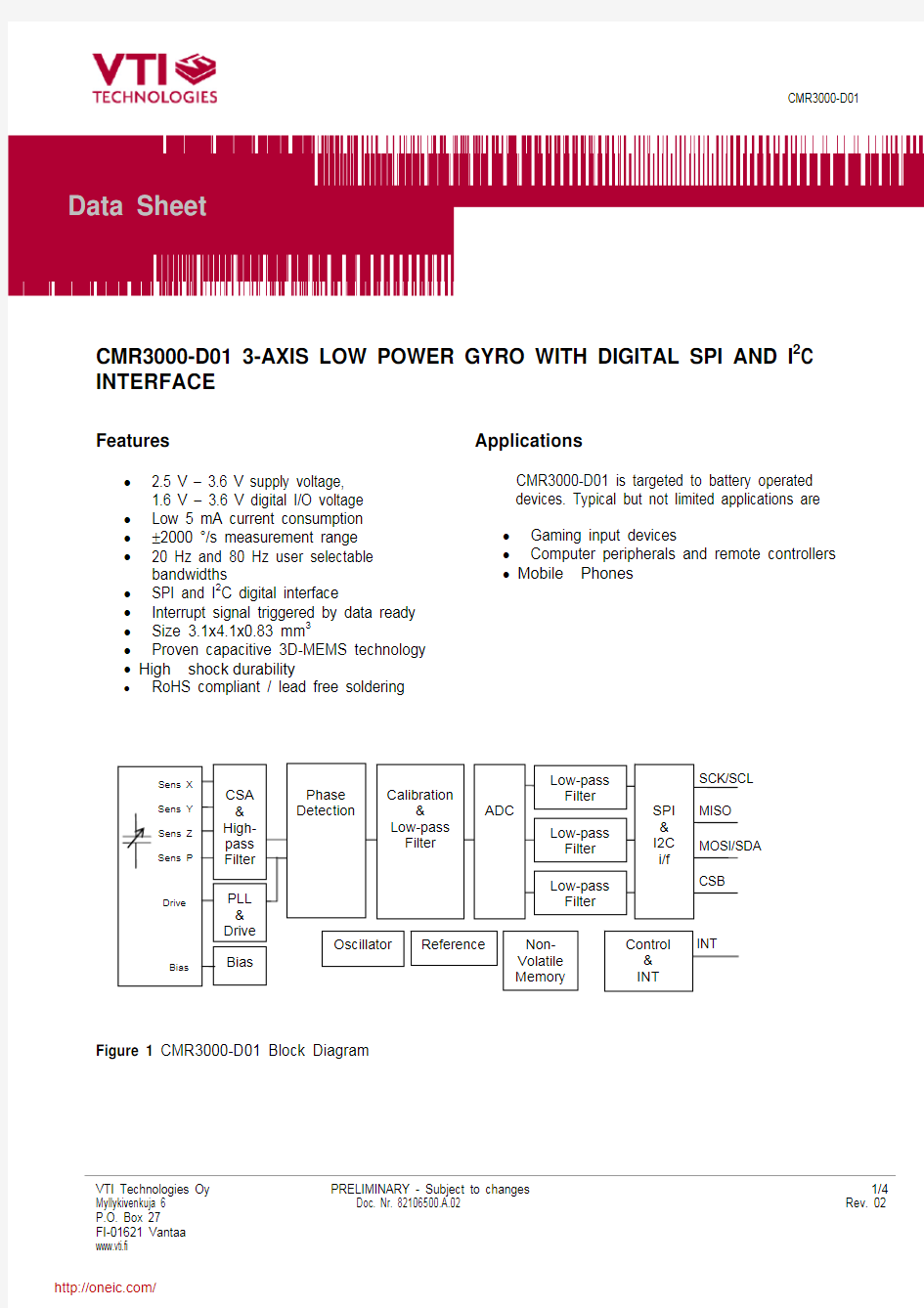
Figure 1 CMR3000-D01 Block Diagram Data Sheet
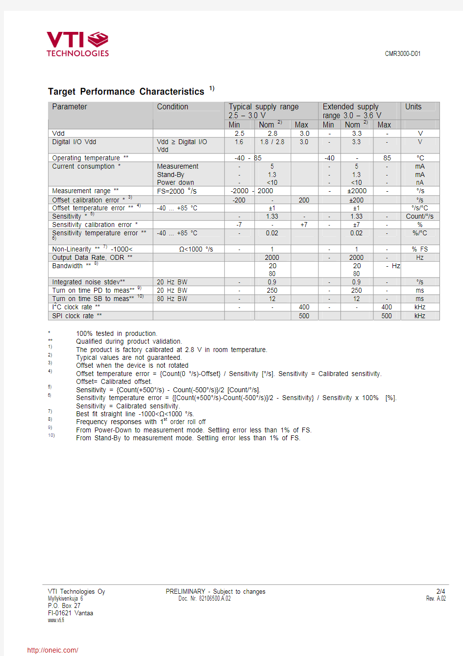
VTI Technologies Oy PRELIMINARY - Subject to changes 2/4Target Performance Characteristics 1)
Typical supply range 2.5 – 3.0 V Extended supply
range 3.0 – 3.6 V Units Parameter
Condition
Min Nom 2) Max
Min Nom 2) Max
Vdd 2.5 2.8 3.0 - 3.3 - V Digital I/O Vdd Vdd ≥ Digital I/O Vdd
1.6 1.8 /
2.8
3.0 - 3.3 - V
Operating temperature ** -40 - 85 -40 - 85 °C Current consumption * Measurement Stand-By Power down - - - 5 1.3 <10 - - - 5 1.3 <10 - - - mA
mA nA
Measurement range ** FS=2000 °/s
-2000 - 2000 - ±2000 - °/s Offset calibration error * 3)
-200 - 200 ±200 °/s
Offset temperature error ** 4)
-40 ... +85 °C ±1 ±1 °/s/°C
Sensitivity * 5)
- 1.33 - - 1.33 - Count/°/s Sensitivity calibration error * -7 - +7 - ±7 - % Sensitivity temperature error ** 6)
-40 ... +85 °C - 0.02 0.02 - %/°C Non-Linearity ** 7) -1000
Bandwidth ** 8)
20 80 20 80
- Hz
Integrated noise stdev** 20 Hz BW - 0.9 - 0.9 - °/s
Turn on time PD to meas** 9)
20 Hz BW - 250 - 250 - ms
Turn on time SB to meas** 10)
80 Hz BW - 12 - 12 - ms I 2
C clock rate ** - - 400 - - 400 kHz SPI clock rate ** 500 500 kHz
* 100% tested in production.
** Qualified during product validation.
1) The product is factory calibrated at 2.8 V in room temperature. 2) Typical values are not guaranteed. 3) Offset when the device is not rotated
4) Offset temperature error = {Count(0 °/s)-Offset} / Sensitivity [°/s]. Sensitivity = Calibrated sensitivity.
Offset= Calibrated offset.
5) Sensitivity = {Count(+500°/s) - Count(-500°/s)}/2 [Count/°/s].
6)
Sensitivity temperature error = {[Count(+500°/s)-Count(-500°/s)]/2 - Sensitivity} / Sensitivity x 100% [%].
Sensitivity = Calibrated sensitivity.
7) Best fit straight line -1000
Frequency responses with 1st order roll off
9)
From Power-Down to measurement mode. Settling error less than 1% of FS. 10)
From Stand-By to measurement mode. Settling error less than 1% of FS.
VTI Technologies Oy PRELIMINARY - Subject to changes 3/4
Figure 2 Package dimensions in mm
SPI
Figure 3 Application schematics for I 2C and SPI bus
VTI Technologies Oy PRELIMINARY - Subject to changes 4/4
Figure 4 Recommended layout pattern (not actual size, for reference only)
Table 1 Pin descriptions (top view)
Pin # Name
Function
1 DVSS Digital ground
2 INT Interrupt
3 MOSI_SDA SPI Serial Data Input (MOSI) / I 2C Serial Data (SDA)
4 CSB
Chip select / I 2C enable 5 AVSS Analog ground 6 AVDD Analog supply voltage
7 SCK_SCL SPI Serial Clock (SCK) / I 2C Serial Clock (SCL)
8 MISO
SPI Serial Data Output (MISO) / I2C slave address LSB ADDR[0] 9 DVIO I/O Supply 10 DVDD
Digital supply voltage
Document Change Control
Rev. Date Change Description 0.1 04-May-09 1st version 0.2 04-Sep-09 Block diagram, package dimensions & layout pattern added 0.3 01-Oct-10 Package dimensions updated 0.4 09-Apr-10 Target Performance Characteristics updated 0.5 20-May-10 Target Performance Characteristics, Table 1, Figure 3 updated 0.6 01-Oct-10 Target Performance Characteristics updated A.01 03-Nov-10 Fig.2 updated, Target Performance Characteristics updated A.02 25-Mar-11 Target Performance Characteristics updated
分销商库存信息: MURATA
CMR3000-D01