HD74LV123A
Dual Retriggerable Monostable Multivibrators
ADE-205-258C (Z)
4th Edition
January 2001 Description
The HD74LV123A features output pulse-duration control by three methods. In the first method, the A input is low and the B input goes high. In the second method, the B input is high and the A input goes low. In the third method, the A input is low, the B input is high, and the clear (CLR) input goes high.
The basic pulse duration is programmed by selecting external resistance and capacitance values.
The external timing capacitor must be connected between Cext and Rext/Cext (positive) and an external resistor connected between Rext/Cext and Vcc
To obtain variable pulse durations, connect an external variable resistance between Rext/Cext and Vcc. Once triggered, the basic pulse duration can be extended by retriggering the gated low-level-active (A) or high-level-active (B) input. Pulse duration can be reduced by taking CLR low.
Features
?V CC = 2.0 V to 5.5 V operation
?All inputs V IH (Max.) = 5.5 V (@V CC = 0 V to 5.5 V)
?All outputs V O (Max.) = 5.5 V (@V CC = 0 V)
?Output current ±6 mA (@V CC = 3.0 V to 3.6 V), ±12 mA (@V CC = 4.5 V to 5.5 V)
HD74LV123A
Rev.4, Jan. 2001, page 2 of 19
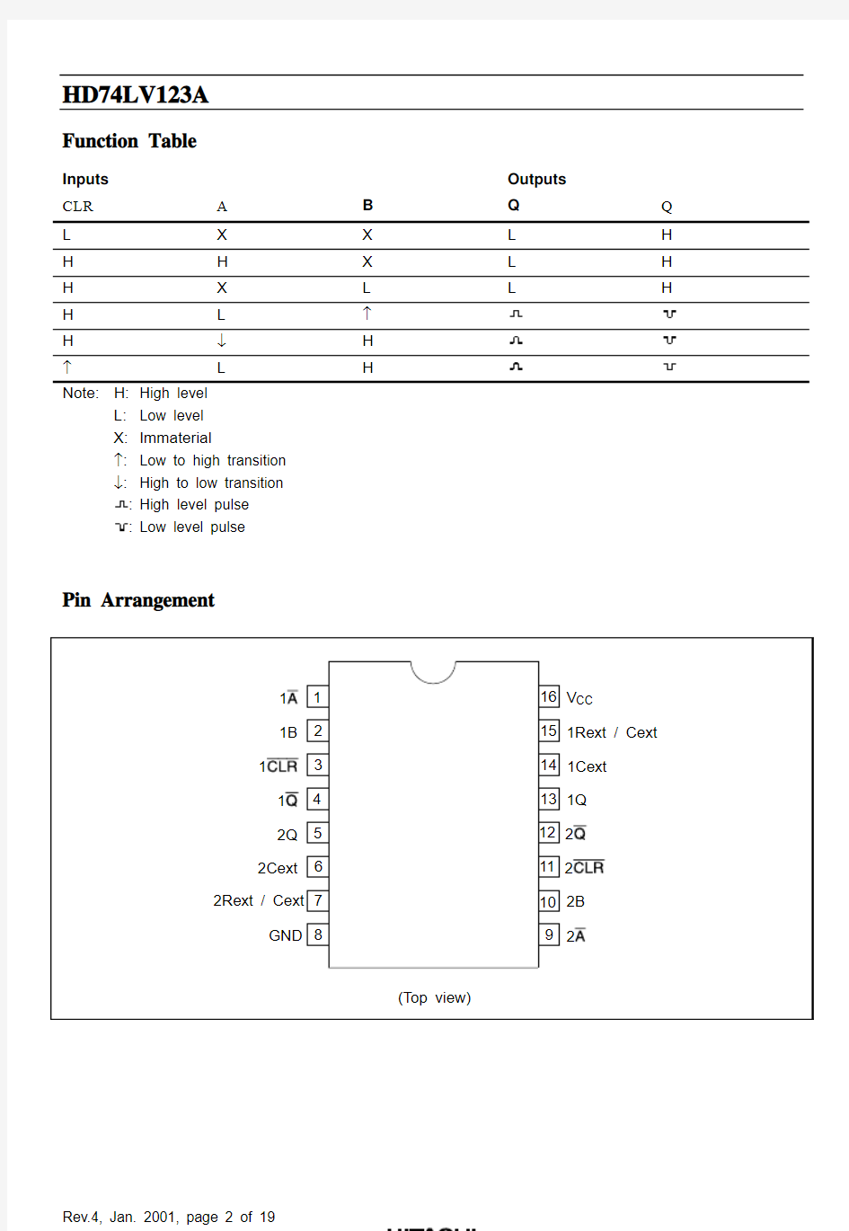
Function Table
Inputs Outputs CLR A B Q Q L X X L H H H X L H H X L L
H
H L
↑H ↓
H ↑L
H
Note:H:
High level L:Low level X:Immaterial
↑:Low to high transition ↓:High to low transition :High level pulse :
Low level pulse
Pin Arrangement
HD74LV123A
Rev.4, Jan. 2001, page 3 of 19
Absolute Maximum Ratings
Item
Symbol Ratings Unit Conditions
Supply voltage range V CC –0.5 to 7.0V Input voltage range *
1V I –0.5 to 7.0V Output voltage range *V O –0.5 to V CC + 0.5V Output: H or L –0.5 to 7.0V CC : OFF Input clamp current I IK –20mA V I < 0
Output clamp current
I OK ±50mA V O < 0 or V O > V CC Continuous output current I O
±25mA V O = 0 to V CC
Continuous current through V CC or GND
I CC or I GND ±50mA Maximum power dissipation
at Ta = 25°C (in still air)*3
P T
785mW
SOP 500
TSSOP
Storage temperature
Tstg –65 to 150°C
Notes:The absolute maximum ratings are values which must not individually be exceeded, and furthermore,
no two of which may be realized at the same time.
1.The input and output voltage ratings may be exceeded if the input and output clamp-current
ratings are observed.
2.This value is limited to 5.5 V maximum.
3.The maximum package power dissipation was calculated using a junction temperature of 150°C.
HD74LV123A
Recommended Operating Conditions
Item Symbol Min Typ Max Unit Conditions Supply voltage range V CC 2.0— 5.5V
Input voltage range V I0— 5.5V
Output voltage range V O0—V CC V
Output current I OH——–50μA V CC = 2.0 V
——–2mA V CC = 2.3 to 2.7 V
——–6V CC = 3.0 to 3.6 V
——–12V CC = 4.5 to 5.5 V
I OL——50μA V CC = 2.0 V
——2mA V CC = 2.3 to 2.7 V
——6V CC = 3.0 to 3.6 V
——12V CC = 4.5 to 5.5 V Input transition rise or fall rate?t /?v0—200ns/V V CC = 2.3 to 2.7 V
0—100V CC = 3.0 to 3.6 V
0—20V CC = 4.5 to 5.5 V External timing registance Rext5——k?V CC = 2.0 V
1——V CC≥ 2.3 V External timing capacitance Cext—Unlimited—F
Power-up ramp rate?t /?V CC1——ms/V
Operating free-air temperature Ta–40—85°C
Note:Unused or floating inputs must be held high or low.
Rev.4, Jan. 2001, page 4 of 19
HD74LV123A Logic Diagram
Rev.4, Jan. 2001, page 5 of 19
HD74LV123A
Rev.4, Jan. 2001, page 6 of 19
DC Electrical Characteristics
Ta = –40 to 85°C
Item Symbol V CC (V)*Min Typ Max Unit Test Conditions
Input voltage
V IH
2.0 1.5——V
2.3 to 2.7V CC × 0.7——
3.0 to 3.6
V CC × 0.7——
4.5 to
5.5V CC × 0.7——V IL
2.0——0.52.3 to 2.7——V CC × 0.3
3.0 to 3.6——V CC × 0.3
4.5 to
5.5
——V CC × 0.3Output voltage
V OH
Min to Max V CC – 0.1——V
I OH = –50 μA 2.3 2.0——I OH = –2 mA 3.0 2.48——I OH = –6 mA 4.5
3.8——I OH = –12 mA V OL
Min to Max ——0.1I OL = 50 μA 2.3——0.4I OL = 2 mA 3.0
——0.44I OL = 6 mA
4.5——0.55I OL = 12 mA Input current I IN 0 to
5.5——±1μA V IN = 5.5 V or GND Input current Rext / Cext I IN 5.5——±2.5μA V IN = V CC or GND Quiescent supply current I CC 5.5——20μA V IN = V CC or GND, I O = 0Active state supply current (per circuit)
?I CC
2.3
—
—
220
μA V IN = V CC or GND Rext/Cext = 0.5 V CC
3.0——280
4.5——650
5.5
——975Output leakage current I OFF 0——5μA V O = 5.5 V Input
capacitance
C IN
3.3
—
4.0
—
pF
V I = V CC or GND
Note:For conditions shown as Min or Max, use the appropriate values under recommended operating
conditions.
HD74LV123A
Rev.4, Jan. 2001, page 7 of 19
Switching Characteristics
V CC = 2.5 ± 0.2 V
Ta = 25°C
Ta = –40 to 85°C Item Symbol Min Typ Max Min Max Unit Test Conditions FROM (Input)TO
(Output)Propa-gation delay time
t PLH t PHL
—
13.5
31.4
1.0
37.0
ns
C L = 15 pF
A or B
Q or Q
—16.036.0 1.042.0C L = 50 pF —11.025.0 1.029.5C L = 15 pF CLR
Q or Q
—13.032.8 1.034.5C L = 50 pF —14.033.4 1.039.0C L = 15 pF CLR Q or Q
—
16.038.0 1.044.0C L = 50 pF
(Trigger)
Output pulse width
t wQ
—
170
260
—
320
ns
C L = 50 pF,
Cext = 28 pF, Rext = 2 k ?9010011090110μs C L = 50 pF,
Cext = 0.01 μF, Rext = 10 k ?0.9
1.0 1.10.9 1.1ms C L = 50 pF,
Cext = 0.1 μF, Rext = 10 k ??t wQ
—±1———%C L = 50 pF Pulse width t w 6.0—— 6.5—ns A , B or CLR
Retrigger time
t rr
—40———ns A , or B
(Rext = 1 k ?, Cext = 100 pF)—
1.5
—
—
—
μs
A , or B
(Rext = 1 k ?, Cext = 0.01 μF)
HD74LV123A
Rev.4, Jan. 2001, page 8 of 19
Switching Characteristics (cont)
V CC = 3.3 ± 0.3 V
Ta = 25°C
Ta = –40 to 85°C Item Symbol Min Typ Max Min Max Unit Test Conditions FROM (Input)TO
(Output)Propa-gation delay time
t PLH t PHL
—
9.7
20.6
1.0
24.0
ns
C L = 15 pF
A or B
Q or Q
—11.524.1 1.027.5C L = 50 pF —8.015.8 1.018.5C L = 15 pF CLR
Q or Q
—9.519.3 1.022.0C L = 50 pF —9.922.4 1.026.0C L = 15 pF CLR Q or Q
—
11.525.9 1.029.5C L = 50 pF
(Trigger)
Output pulse width
t wQ
—
150
240
—
300
ns
C L = 50 pF,
Cext = 28 pF, Rext = 2 k ?9010011090110μs C L = 50 pF,
Cext = 0.01 μF, Rext = 10 k ?0.9
1.0 1.10.9 1.1ms C L = 50 pF,
Cext = 0.1 μF, Rext = 10 k ??t wQ
—±1———%C L = 50 pF Pulse width t w 5.0—— 5.0—ns A , B or CLR
Retrigger time
t rr
—30———ns A , or B
(Rext = 1 k ?, Cext = 100 pF)—
1.2
—
—
—
μs
A , or B
(Rext = 1 k ?, Cext = 0.01 μF)
HD74LV123A
Rev.4, Jan. 2001, page 9 of 19
Switching Characteristics (cont)
V CC = 5.0 ± 0.5 V
Ta = 25°C
Ta = –40 to 85°C Item Symbol Min Typ Max Min Max Unit Test Conditions FROM (Input)TO
(Output)Propa-gation delay time
t PLH t PHL
—
7.3
12.0
1.0
14.0
ns
C L = 15 pF
A or B
Q or Q
—8.514.0 1.016.0C L = 50 pF — 5.99.4 1.011.0C L = 15 pF CLR
Q or Q
—7.511.4 1.013.0C L = 50 pF —7.312.9 1.015.0C L = 15 pF CLR Q or Q
—
8.714.9 1.017.0C L = 50 pF
(Trigger)
Output pulse width
t wQ
—
140
200
—
240
ns
C L = 50 pF,
Cext = 28 pF, Rext = 2 k ?9010011090110μs C L = 50 pF,
Cext = 0.01 μF, Rext = 10 k ?0.9
1.0 1.10.9 1.1ms C L = 50 pF,
Cext = 0.1 μF, Rext = 10 k ??t wQ
—±1———%C L = 50 pF Pulse width t w 5.0—— 5.0—ns A , B or CLR
Retrigger time
t rr
—20———ns A , or B
(Rext = 1 k ?, Cext = 100 pF)—
0.95
—
—
—
μs
A , or B
(Rext = 1 k ?, Cext = 0.01 μF)
HD74LV123A
Rev.4, Jan. 2001, page 10 of 19
Operating Characteristics
C L = 50 pF
Ta = 25°C
Item Symbol V CC (V)Min Typ Max Unit Test Conditions Power dissipation capacitance
C PD
3.3
—
74.0
—
pF
f = 10 MHz
5.0—8
6.0—
Test Circuit
HD74LV123A Timing diagram
Rev.4, Jan. 2001, page 11 of 19
HD74LV123A
Rev.4, Jan. 2001, page 12 of 19
HD74LV123A
Rev.4, Jan. 2001, page 13 of 19
HD74LV123A Application Data
Rev.4, Jan. 2001, page 14 of 19
HD74LV123A
Rev.4, Jan. 2001, page 15 of 19
HD74LV123A
Rev.4, Jan. 2001, page 16 of 19
HD74LV123A Package Dimensions
Rev.4, Jan. 2001, page 17 of 19
HD74LV123A
Rev.4, Jan. 2001, page 18 of 19
HD74LV123A
Rev.4, Jan. 2001, page 19 of 19
Disclaimer
1.Hitachi neither warrants nor grants licenses of any rights of Hitachi’s or any third party’s patent,
copyright, trademark, or other intellectual property rights for information contained in this document.Hitachi bears no responsibility for problems that may arise with third party’s rights, including intellectual property rights, in connection with use of the information contained in this document.2.
Products and product specifications may be subject to change without notice. Confirm that you have received the latest product standards or specifications before final design, purchase or use.
3.Hitachi makes every attempt to ensure that its products are of high quality and reliability. However,contact Hitachi’s sales office before using the product in an application that demands especially high quality and reliability or where its failure or malfunction may directly threaten human life or cause risk of bodily injury, such as in aerospace, aeronautics, nuclear power, combustion control, transportation,traffic, safety equipment or medical equipment for life support.
4.Design your application so that the product is used within the ranges guaranteed by Hitachi particularly for maximum rating, operating supply voltage range, heat radiation characteristics, installation
conditions and other characteristics. Hitachi bears no responsibility for failure or damage when used beyond the guaranteed ranges. Even within the guaranteed ranges, consider normally foreseeable failure rates or failure modes in semiconductor devices and employ systemic measures such as fail-safe devices,so that the equipment incorporating the Hitachi product does not cause bodily injury, fire or other consequential damage due to operation of the Hitachi product.5.This product is not designed to be radiation resistant.
6.No one is permitted to reproduce or duplicate, in any form, the whole or part of this document without written approval from Hitachi.
7.Contact Hitachi’s sales office for any questions regarding this document or Hitachi semiconductor products.
Sales Offices
Hitachi, Ltd.
Semiconductor & Integrated Circuits.
Nippon Bldg., 2-6-2, Ohte-machi, Chiyoda-ku, Tokyo 100-0004, Japan Tel: Tokyo (03) 3270-2111 Fax: (03) 3270-5109
Copyright Hitachi, Ltd., 2001. All rights reserved. Printed in Japan.
Hitachi Asia Ltd. Hitachi Tower
16 Collyer Quay #20-00, Singapore 049318
Tel : <65>-538-6533/538-8577 Fax : <65>-538-6933/538-3877URL : https://www.doczj.com/doc/b415011187.html,.sg URL
NorthAmerica : https://www.doczj.com/doc/b415011187.html,/Europe : https://www.doczj.com/doc/b415011187.html,/hel/ecg Asia : https://www.doczj.com/doc/b415011187.html,
Japan : http://www.hitachi.co.jp/Sicd/indx.htm
Hitachi Asia Ltd.
(Taipei Branch Office)
4/F, No. 167, Tun Hwa North Road, Hung-Kuo Building, Taipei (105), Taiwan Tel : <886>-(2)-2718-3666 Fax : <886>-(2)-2718-8180 Telex : 23222 HAS-TP
URL : https://www.doczj.com/doc/b415011187.html,
Hitachi Asia (Hong Kong) Ltd.
Group III (Electronic Components) 7/F., North Tower, World Finance Centre,
Harbour City, Canton Road Tsim Sha Tsui, Kowloon, Hong Kong
Tel : <852>-(2)-735-9218 Fax : <852>-(2)-730-0281
URL : https://www.doczj.com/doc/b415011187.html,
Hitachi Europe Ltd.
Electronic Components Group.Whitebrook Park
Lower Cookham Road Maidenhead
Berkshire SL6 8YA, United Kingdom Tel: <44> (1628) 585000Fax: <44> (1628) 585160
Hitachi Europe GmbH
Electronic Components Group Dornacher Stra§e 3
D-85622 Feldkirchen, Munich Germany
Tel: <49> (89) 9 9180-0Fax: <49> (89) 9 29 30 00Hitachi Semiconductor (America) Inc.
179 East Tasman Drive,San Jose,CA 95134 Tel: <1> (408) 433-1990Fax: <1>(408) 433-0223
For further information write to:
Colophon 2.0