NCP5369
Integrated Driver and MOSFET
The NCP5369 integrates a MOSFET driver, high?side MOSFET and low?side MOSFET into a 6 mm x 6 mm 40?pin QFN package. The driver and MOSFETs have been optimized for high?current DC?DC buck power conversion applications. The NCP5369 integrated solution greatly reduces package parasitics and board space compared to a discrete component solution.
Features
?Capable of Switching Frequencies Up to 1 MHz ?Capable of Output Currents Up to 35 A
?Internal Bootstrap Diode
?Zero Current Detection
?Undervoltage Lockout
?Internal Thermal Warning / Thermal Shutdown
?These are Pb?Free Devices
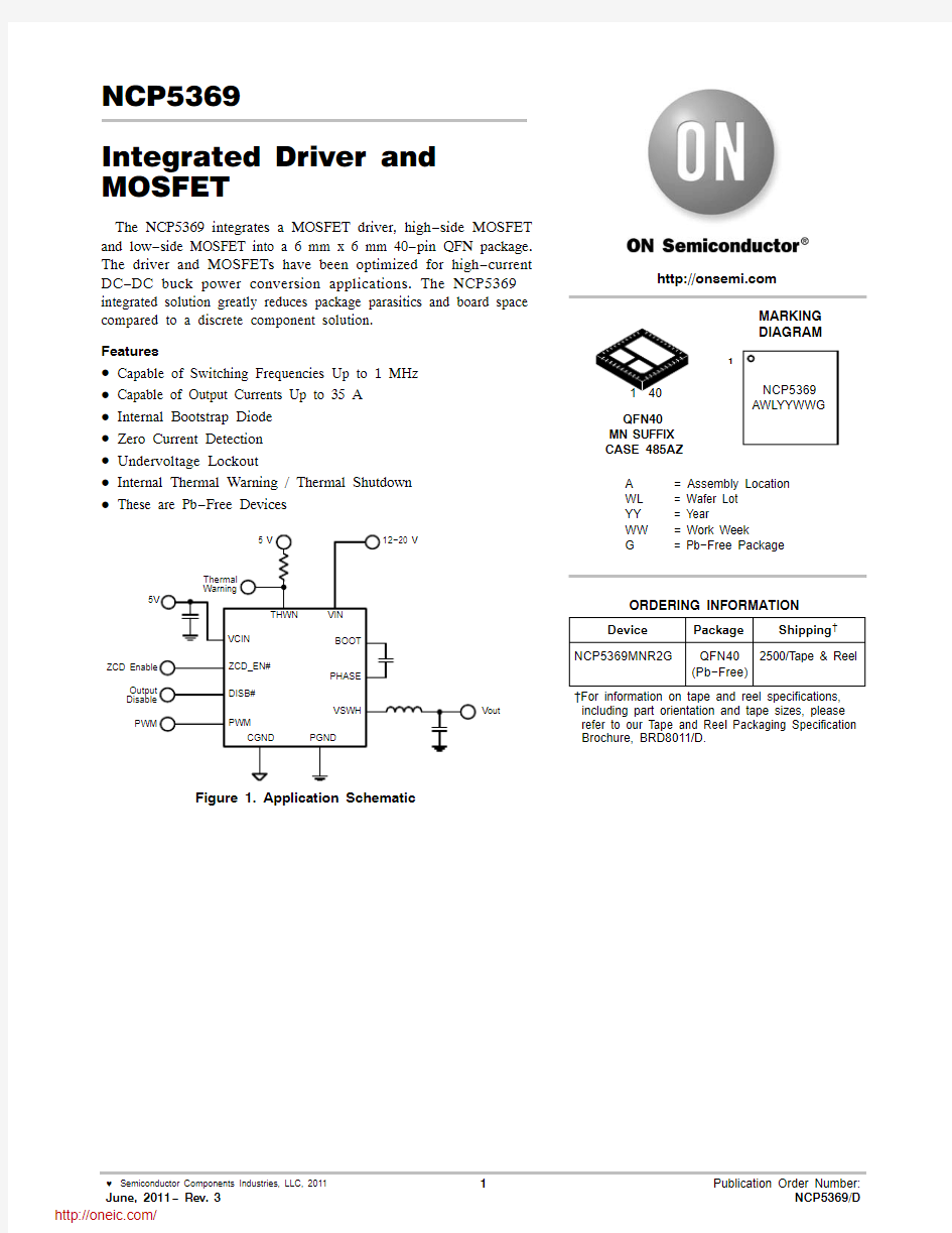
Vout Figure 1. Application Schematic
Device Package Shipping?
ORDERING INFORMATION
QFN40
(Pb?Free)
2500/Tape & Reel NCP5369MNR2G
MARKING
DIAGRAM
QFN40
MN SUFFIX
CASE 485AZ
https://www.doczj.com/doc/b513797467.html,
?For information on tape and reel specifications, including part orientation and tape sizes, please refer to our Tape and Reel Packaging Specification Brochure, BRD8011/D.
NCP5369
AWLYYWWG
1
A= Assembly Location
WL= Wafer Lot
YY= Year
WW= Work Week
G= Pb?Free Package
PWM
VCIN
DISB#
VIN
BOOT
GH
GL
ZCD_EN#
THWN
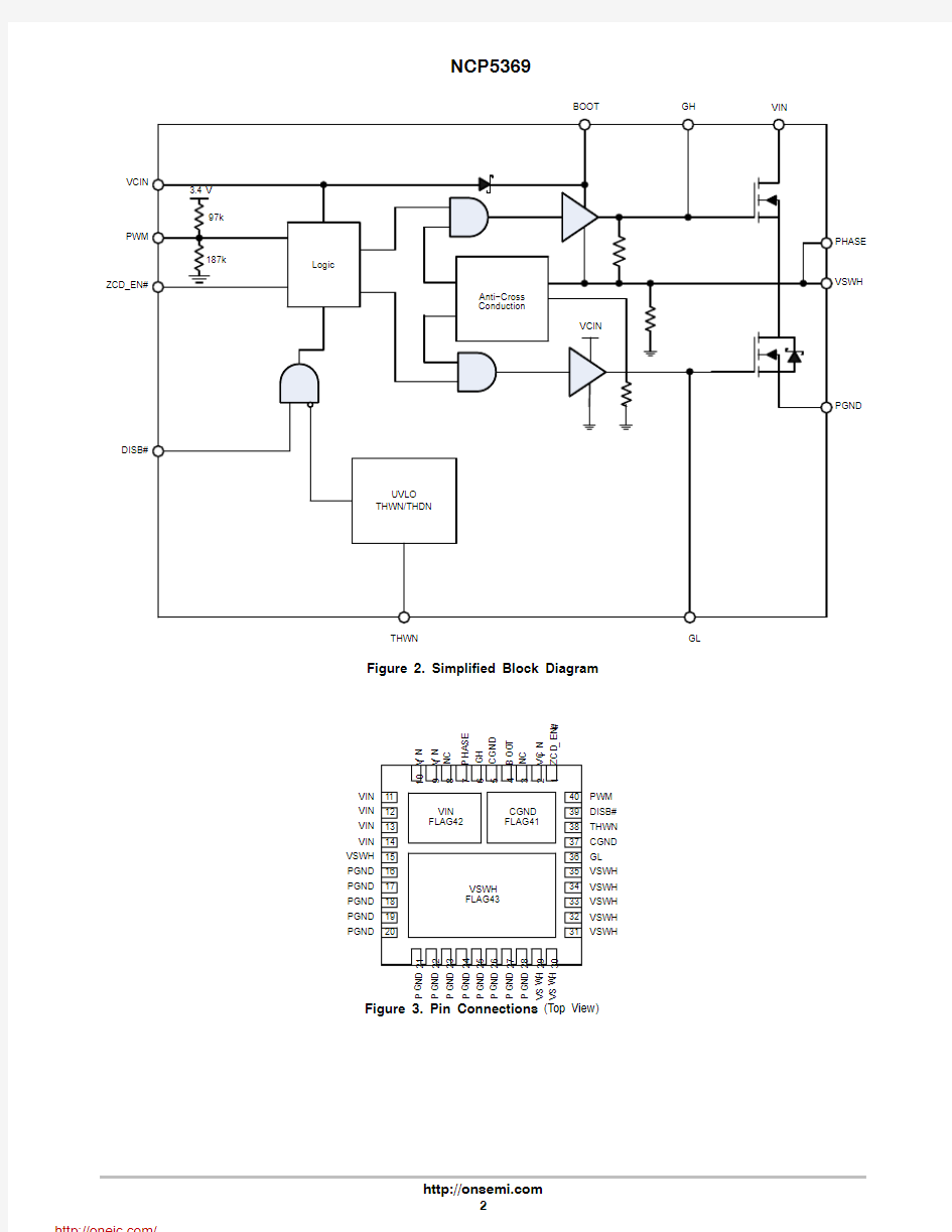
Figure 2. Simplified Block Diagram
PWM DISB#CGND THWN GL VSWH VSWH VSWH
VSWH VSWH VIN VIN VIN VIN VSWH PGND PGND PGND
PGND PGND P G N Figure 3. Pin Connections (Top View)
P G N P G N P G N P G N P G N P G N P G N V S W V S W V I N
V I N N C
P H A S E
G H C G N D
B O O T N C
V C I N
Z C D _E N #
Table 1. PIN FUNCTION DESCRIPTION
Pin No.Pin Name Description
1ZCD_EN#Enable Zero Current Detection
2VCIN Control Input Voltage
3, 8NC No Connect
4BOOT Bootstrap Voltage
5, 37, FLAG 41CGND Control Signal Ground
6GH High Side FET Gate Access
7PHASE Provides a return path for the high side driver of the internal IC. Place a high frequency ceram-
ic capacitor of 0.1 uF to 1.0 uF from this pin to BOOT pin.
9?14, FLAG 42VIN Input Voltage
15, 29?35,
FLAG 43
VSWH Switch Node Output
16?28PGND Power Ground
36GL Low Side FET Gate Access
38THWN Thermal Warning
39DISB#Output Disable Pin
40PWM PWM Drive Logic
Table 2. ABSOLUTE MAXIMUM RATINGS
Symbol Pin Name / Rating Min Max Unit VCIN Control Input Voltage?0.37V VIN Power Input Voltage?0.330V BOOT Bootstrap Voltage?0.3 V wrt/VSWH35 V wrt/PGND
40 V < 50 ns wrt/PGND
7 V wrt/VSWH
V
VSWH Switch Node Output?5 V
?10 V < 200 ns
35 V
40 V < 50 ns
V
ZCD_EN#Zero Current Detection?0.3 6.5V PWM PWM Drive Logic?0.3 6.5V DISB#Output Disable?0.3 6.5V THWN Thermal Warning?0.3 6.5V T J Junction Temperature?55 to 150°C T S Storage Temperature?55 to 150°C R q JPCB Thermal Resistance, High?Side FET13°C/W R q JPCB Thermal Resistance, Low?Side FET5°C/W MSL Moisture Sensitivity Level3
Stresses exceeding Maximum Ratings may damage the device. Maximum Ratings are stress ratings only. Functional operation above the Recommended Operating Conditions is not implied. Extended exposure to stresses above the Recommended Operating Conditions may affect device reliability.
Table 3. OPERATING RANGES
Rating Symbol Min Typ Max Unit Control Input Voltage VCIN 4.55 5.5V Input Voltage VIN 4.51225V
ELECTRICAL CHARACTERISTICS (Note 1) (VCIN = 5 V, VIN = 12 V, T A = ?10°C to +100°C, unless otherwise noted) Parameter Symbol Condition Min Typ Max Unit SUPPLY CURRENT
1420mA VCIN Current (normal mode)?DISB# = 5 V, PWM = OSC,
FSW = 400 kHz
VCIN Current (shutdown mode)?DISB# = GND1530m A UNDERVOLTAGE LOCKOUT
UVLO Startup? 3.8 4.35 4.5V UVLO Hysteresis?150200250mV BOOTSTRAP DIODE
Forward Voltage?VCIN = 5 V, forward bias current = 2 mA0.10.40.6V PWM INPUT
PWM Input Voltage High V PWM_HI 3.6??V PWM Input Voltage Mid?State V PWM_MID 1.3? 3.0V PWM Input Voltage Low V PWM_LO??0.7V Tri?State Shutdown Holdoff Time t holdoff250ns PWM Input Resistance63k W PWM Input Bias Voltage 2.2V OUTPUT DISABLE
Output Disable Input Voltage High V DISB#_HI 2.0??V Output Disable Input Voltage Low V DISB#_LO??0.8V Output Disable Hysteresis??500?mV Output Disable Propagation Delay?2040ns ZERO CROSS DETECT
Zero Cross Detect High V ZCD_EN#_HI 2.0??V Zero Cross Detect Low V ZCD_EN#_LO??0.8V Zero Cross Detect Threshold?6mV ZCD Blanking Timer250ns THERMAL WARNING/SHUTDOWN
Thermal Warning Temperature150°C Thermal Warning Hysteresis15°C Thermal Shutdown Temperature180°C Thermal Shutdown Hysteresis25°C 1.Performance guaranteed over the indicated operating temperature range by design and/or characterization tested at T J = T A = 25°C. Low
duty cycle pulse techniques are used during testing to maintain the junction temperature as close to ambient as possible.
APPLICATIONS INFORMATION
Theory of Operation
The NCP5369 is an integrated driver and MOSFET module designed for use in a synchronous buck converter topology. A single PWM input signal is all that is required to properly drive the high?side and low?side MOSFETs. Low?Side Driver
The low?side driver is designed to drive a ground?referenced low R DS(on) N?Channel MOSFET. The voltage rail for the low?side driver is internally connected to VCIN and PGND.
High?Side Driver
The high?side driver is designed to drive a floating low RDS(on) N?channel MOSFET. The gate voltage for the high side driver is developed by a bootstrap circuit referenced to Switch Node (VSWH) pin.
The bootstrap circuit is comprised of the internal diode and an external bootstrap capacitor. When the NCP5369 is starting up, the VSWH pin is at ground, so the bootstrap capacitor will charge up to VCIN through the bootstrap diode See Figure 1. When the PWM input goes high, the high?side driver will begin to turn on the high?side MOSFET using the stored charge of the bootstrap capacitor. As the high?side MOSFET turns on, the VSWH pin will rise. When the high?side MOSFET is fully on, the switch node will be at 12 V, and the BST pin will be at 5 V plus the charge of the bootstrap capacitor (approaching 17 V). The bootstrap capacitor is recharged when the switch node goes low during the next cycle.
Zero Current Detect
When ZCD_EN# is set high, the NCP5369 will operate in normal PWM mode.
When ZCD_EN# is set low, zero current detect (ZCD) will be enabled. If PWM goes high, GH will go high after the non?overlap delay. If PWM goes low, GL will go high after the non?overlap delay, and stay high for the duration of the ZCD blanking timer. Once this timer has expired, VSWH will be monitored for zero current detection, and will pull GL low once detected. The threshold on VSWH to determine zero current undergoes an auto-calibration cycle every time DISB# is brought from low to high. This auto-calibration cycle typically takes 55 m s to complete. Safety Timer and Overlap Protection Circuit
It is very important that MOSFETs in a synchronous buck regulator do not both conduct at the same time. Excessive shoot?through or cross conduction can damage the MOSFETs, and even a small amount of cross conduction will cause a decrease in the power conversion efficiency.
The NCP5369 prevents cross conduction by monitoring the status of the MOSFETs and applying the appropriate amount of “dead?time” or the time between the turn off of one MOSFET and the turn on of the other MOSFET. When the PWM input pin goes high, the gate of the low?side MOSFET (GL pin) will go low after a propagation delay (tpdlGL). The time it takes for the low?side MOSFET to turn off (tfGL) is dependent on the total charge on the low?side MOSFET gate. The NCP5369 monitors the gate voltage of both MOSFETs and the switchnode voltage to determine the conduction status of the MOSFETs. Once the low?side MOSFET is turned off an internal timer will delay (tpdhGH) the turn on of the high?side MOSFET. Likewise, when the PWM input pin goes low, the gate of the high?side MOSFET (GH pin) will go low after the propagation delay (tpdlGH). The time to turn off the high?side MOSFET (tfGH) is dependent on the total gate charge of the high?side MOSFET. A timer will be triggered once the high?side MOSFET has stopped conducting, to delay (tpdhGL) the turn on of the low?side MOSFET.
Th ermal Warning / Thermal Shutdown
When the temperature of the driver reaches 150°C, the THWN pin will be pulled low indicating a thermal warning. At this point, the part continues to function normally. When the temperature drops below 135°C, the THWN will go high.
If the driver temperature exceeds 180°C, the part will enter thermal shutdown and turn off both MOSFETs. Once the temperature falls below 155°C, the part will resume normal operation. The THWN pin has a maximum current capability of 30 mA.
Power Supply Decoupling
The NCP5369 can source and sink relatively large current to the gate pins of the MOSFETs. In order to maintain a constant and stable supply voltage (VCIN) a low ESR capacitor should be placed near the power and ground pins.
A 1 m F to 4.7 m F multi layer ceramic capacitor (MLCC) is usually sufficient.
Bootstrap Circuit
The bootstrap circuit uses a charge storage capacitor (C BST) and the internal diode. The bootstrap capacitor must have a voltage rating that is able to withstand twice the maximum supply voltage. A minimum 50 V rating is recommended. A bootstrap capacitance greater than 100 nF and a minimum 50 V rating is recommended. A good quality ceramic capacitor should be used.
ZCD_EN#
PWM
IL
GL
GH
Figure 4. Zero Current Detection
PWM
GL
GH
Figure 5. Tri ?State Operation
PACKAGE DIMENSIONS
QFN40 6x6, 0.5P
MN SUFFIX
CASE 485AZ?01
ISSUE O
NOTES:
1.DIMENSIONING AND TOLERANCING PER
ASME Y14.5M, 1994.
2.CONTROLLING DIMENSIONS: MILLIMETERS.
3.DIMENSION b APPLIES TO PLATED
TERMINAL AND IS MEASURED BETWEEN
0.15 AND 0.30mm FROM TERMINAL
4.COPLANARITY APPLIES TO THE EXPOSED
PAD AS WELL AS THE TERMINALS.
5.POSITIONAL TOLERANCE APPLIES TO ALL
THREE EXPOSED PADS.
DIM MIN MAX
MILLIMETERS
A0.80 1.00
A1???0.05
A30.20 REF
b0.180.30
D 6.00 BSC
D2 2.30 2.50
E 6.00 BSC
4.50
E2 4.30
e0.50 BSC
L0.300.50
K0.20???
D3 1.40 1.60
2.10
E3 1.90
L1???0.15
L1
DETAIL A
L
ALTERNATE
CONSTRUCTIONS
DETAIL B
ALTERNATE
CONSTRUCTION
G 2.20 BSC
DIMENSIONS: MILLIMETERS
PKG
ON Semiconductor and are registered trademarks of Semiconductor Components Industries, LLC (SCILLC). SCILLC reserves the right to make changes without further notice to any products herein. SCILLC makes no warranty, representation or guarantee regarding the suitability of its products for any particular purpose, nor does SCILLC assume any liability arising out of the application or use of any product or circuit, and specifically disclaims any and all liability, including without limitation special, consequential or incidental damages.
“Typical” parameters which may be provided in SCILLC data sheets and/or specifications can and do vary in different applications and actual performance may vary over time. All operating parameters, including “Typicals” must be validated for each customer application by customer’s technical experts. SCILLC does not convey any license under its patent rights nor the rights of others. SCILLC products are not designed, intended, or authorized for use as components in systems intended for surgical implant into the body, or other applications intended to support or sustain life, or for any other application in which the failure of the SCILLC product could create a situation where personal injury or death may occur. Should Buyer purchase or use SCILLC products for any such unintended or unauthorized application, Buyer shall indemnify and hold SCILLC and its officers, employees, subsidiaries, affiliates, and distributors harmless against all claims, costs, damages, and expenses, and reasonable attorney fees arising out of, directly or indirectly, any claim of personal injury or death associated with such unintended or unauthorized use, even if such claim alleges that SCILLC was negligent regarding the design or manufacture of the part. SCILLC is an Equal Opportunity/Affirmative Action Employer. This literature is subject to all applicable copyright laws and is not for resale in any manner.
PUBLICATION ORDERING INFORMATION
分销商库存信息: ONSEMI
NCP5369MNR2G