Parameter
Typ.
Max.
Units
R θJA
Maximum Junction-to-Ambient
75
100
°C/W
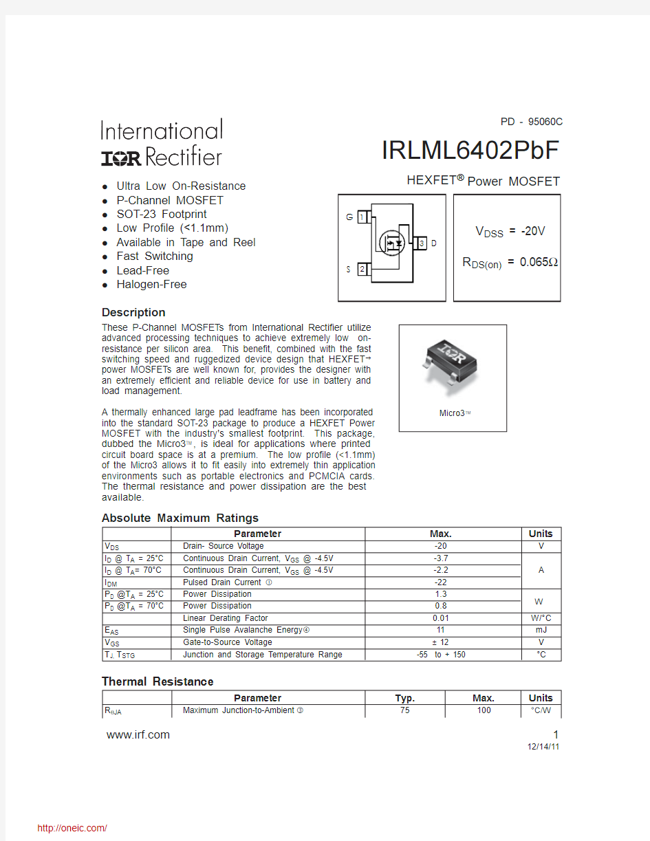
These P-Channel MOSFETs from International Rectifier utilize advanced processing techniques to achieve extremely low on-resistance per silicon area. This benefit, combined with the fast switching speed and ruggedized device design that HEXFET ?power MOSFETs are well known for, provides the designer with an extremely efficient and reliable device for use in battery and load management.
A thermally enhanced large pad leadframe has been incorporated into the standard SOT-23 package to produce a HEXFET Power MOSFET with the industry's smallest footprint. This package,dubbed the Micro3?, is ideal for applications where printed circuit board space is at a premium. The low profile (<1.1mm)of the Micro3 allows it to fit easily into extremely thin application environments such as portable electronics and PCMCIA cards.The thermal resistance and power dissipation are the best available.
Thermal Resistance
l
Ultra Low On-Resistance l P-Channel MOSFET l SOT-23 Footprint l Low Profile (<1.1mm)
l Available in Tape and Reel l Fast Switching l Lead-Free l Halogen-Free
Description
12/14/11
https://www.doczj.com/doc/b46666828.html, 1
Parameter
Max.
Units
V DS
Drain- Source Voltage
-20V I D @ T A = 25°C Continuous Drain Current, V GS @ -4.5V -3.7I D @ T A = 70°C Continuous Drain Current, V GS @ -4.5V -2.2A I DM
Pulsed Drain Current -22P D @T A = 25°C Power Dissipation 1.3P D @T A = 70°C Power Dissipation 0.8Linear Derating Factor
0.01W/°C E AS Single Pulse Avalanche Energy 11mJ V GS
Gate-to-Source Voltage
± 12V T J, T STG
Junction and Storage Temperature Range
-55 to + 150
°C
Absolute Maximum Ratings
W Micro3?
IRLML6402PbF
https://www.doczj.com/doc/b46666828.html,
Repetitive rating; pulse width limited by max. junction temperature.
Notes:
Pulse width ≤ 400μs; duty cycle ≤ 2%.
Source-Drain Ratings and Characteristics
** For recommended footprint and soldering techniques refer to application note #AN-994.
Surface mounted on 1" square single layer 1oz. copper FR4 board,
steady state.
Starting T J = 25°C, L = 1.65mH
R G = 25Ω, I AS = -3.7A.
Parameter
Min.Typ.Max.Units Conditions V (BR)DSS
Drain-to-Source Breakdown Voltage -20––––––V V GS = 0V, I D = -250μA
ΔV (BR)DSS /ΔT J
Breakdown Voltage Temp. Coefficient –––-0.009–––V/°C Reference to 25°C, I D = -1mA –––0.0500.065V GS = -4.5V, I D = -3.7A
–––0.0800.135V GS = -2.5V, I D = -3.1A V GS(th)Gate Threshold Voltage -0.40-0.55-1.2V V DS = V GS , I D = -250μA g fs Forward Transconductance 6.0––––––S V DS = -10V, I D = -3.7A ––––––-1.0V DS = -20V, V GS = 0V
––––––-25V DS = -20V, V GS = 0V, T J = 70°C Gate-to-Source Forward Leakage ––––––-100V GS = -12V
Gate-to-Source Reverse Leakage ––––––100V GS = 12V Q g Total Gate Charge
–––8.012I D = -3.7A Q gs Gate-to-Source Charge
––– 1.2 1.8nC V DS = -10V Q gd Gate-to-Drain ("Miller") Charge ––– 2.8 4.2V GS = -5.0V t d(on)Turn-On Delay Time –––350–––V DD = -10V t r Rise Time
–––48–––I D = -3.7A
t d(off)Turn-Off Delay Time –––588–––R G = 89Ωt f Fall Time
–––381–––R D = 2.7ΩC iss Input Capacitance –––633–––V GS = 0V C oss Output Capacitance
–––145–––pF V DS = -10V C rss
Reverse Transfer Capacitance
–––110–––? = 1.0MHz
Electrical Characteristics @ T J = 25°C (unless otherwise specified)
I GSS μA
Ω
R DS(on)Static Drain-to-Source On-Resistance I DSS Drain-to-Source Leakage Current nA
ns
IRLML6402PbF
https://www.doczj.com/doc/b46666828.html, 3
Vs. Temperature
IRLML6402PbF
https://www.doczj.com/doc/b46666828.html,
Gate-to-Source Voltage
Fig 5. Typical Capacitance Vs.
Drain-to-Source Voltage Forward Voltage
1
10
100
V DS , Drain-to-Source Voltage (V)
0200
400600
800
1000
C , C a p a c i t a n c e (p F )
IRLML6402PbF
https://www.doczj.com/doc/b46666828.html, 5
Fig 11. Maximum Effective Transient Thermal Impedance, Junction-to-Ambient
Case Temperature
Vs. Drain Current
IRLML6402PbF
https://www.doczj.com/doc/b46666828.html,
Fig 13. Typical On-Resistance Vs.
Drain Current
Fig 12. Typical On-Resistance Vs.
Gate Voltage 2.0
3.0
4.0
5.0
6.0
7.0
-V GS, Gate -to -Source Voltage ( V )
0.02
0.04
0.06
0.08
0.10
0.12
0.14
R D S (o n ) , D r a i n -t o -S o u r c e V o l t a g e ( Ω
)
5
10
15
20
25
30
-I D , Drain Current ( A )
0.00
0.04
0.08
0.12
0.16
0.20
R D S ( o n ) , D r a i n -t o -S o u r c e O n R e s i s t a n c e ( Ω )
IRLML6402PbF
https://www.doczj.com/doc/b46666828.html, 7
Micro3 (SOT-23/TO-236AB) Part Marking Information
Micro3 (SOT-23) Package Outline
Dimensions are shown in millimeters (inches)
Note: For the most current drawing please refer to IR website at: https://www.doczj.com/doc/b46666828.html,/package/
1. DIMENSIONING & TOLERANCING PER ANSI Y14.5M-1994
2. DIMEN SION S ARE SHOWN IN MILLIMETERS [INCHES].
3. CONTROLLING D IMENSION: MILLIMETER.
4. DATUM PLAN E H IS LOCATED AT THE MOLD PARTING LIN E.
5. DATUM A AND B TO BE DETERMIN ED AT DATUM PLANE H.
6. D IMENSIO NS D AND E1 ARE MEASUR ED AT DATUM PLANE H. DIMENSION S D OES NO T INCLUDE MOLD PR OTRUSIO NS O R IN TER LEAD FLASH. MOLD PROTRUSIO NS O R INTERLEAD FLASH SHALL NOT EXCEED 0.25 MM [0.010 INCH] PER SIDE.
7. DIMENSION L IS THE LEAD LENGTH FOR SOLDERING TO A SUBSTRATE.
8. OUTLINE CON FO RMS TO JEDEC O UTLINE TO-236 AB.
0.89 1.12SYMBOL
MAX
MIN
A1b 0.010.10c 0.300.50D 0.080.20E 2.80 3.04E1 2.10 2.64e 1.20 1.40A 0.95BSC L 0.400.6008MILLIMETERS A20.88 1.02e1 1.90BSC REF 0.54L1BSC 0.25L2
BSC ! REF 7T8? &$ # "$INCHES 8
0 !# %7T8 "& $$ #& # '" ! ' " ! ! #0.0004MIN
MAX
## "$DIMENSIONS
Recommended Footprint
F = IRLM L6401A 2001A 27Notes: T his pa rt ma rking informa tion a pplies to de vic e s p roduce d a fte r 02/26/2001
ODE
LEA D FREE
DA TE C E = IRLML6402X = PA RT NUM BER CODE REFERENCE:
D = IRLML5103C = IRLML6302B = IRLML2803A = IRLM L2402W = (1-26) IF PRECEDED BY LA ST DIG IT OF C A LENDA R YEA R
W = (27-52) IF PRECEDED BY A LETTER
Y 820083*********YEA R 20022520052004420072006762010
20099YEA R Y C 03WORK WEEK 0102A W B 04
D
242625Z
Y WORK WEEK W H = IRLM L5203G = IRLM L2502K
H G F E D C B 20062003200220052004200820072010
2009J 292830
C B D
50I = IRLML0030J = IRLM L2030L = IRLML0060M = IRLML0040K = IRLML0100N = IRLM L2060P = IRLML9301R = IRLML9303
Cu W IRE
HA LOG PA
IRLML6402PbF
https://www.doczj.com/doc/b46666828.html,
Micro3?(SOT-23/TO-263AB) T ape & Reel Information
Dimensions are shown in millimeters
(inches)
2.05 ( .080 )1.95 ( .077 )
TR
FEED DIRECTION
4.1 ( .161 )3.9 ( .154 )
1.6 ( .062 )1.5 ( .060 )
1.85 ( .072 )1.65 ( .065 )
3.55 ( .139 )3.45 ( .136 )
1.1 ( .043 )0.9 ( .036 )4.1 ( .161 )3.9 ( .154 )
0.35 ( .013 )0.25 ( .010 )
8.3 ( .326 )7.9 ( .312 )
1.32 ( .051 )1.12 ( .045 )
9.90 ( .390 )8.40 ( .331 )
178.00( 7.008 ) MAX.
NOTES:
1. CONTROLLING DIMENSION : MILLIMETER.
2. OUTLINE CONFORMS TO EIA-481 & EIA-541.
Data and specifications subject to change without notice.
IR WORLD HEADQUARTERS: 101N.Sepulveda Blvd, El Segundo, California 90245, USA Tel: (310) 252-7105
TAC Fax: (310) 252-7903
Visit us at https://www.doczj.com/doc/b46666828.html, for sales contact information . 12/2011
分销商库存信息: IR
IRLML6402TRPBF