JOURNAL OF LIGHTW A VE TECHNOLOGY ,VOL.18,NO.3,MARCH 2000
273
A Photonic Front-End Processor in a WDM ATM
Multicast Switch
H.J.Chao ,Senior Member,IEEE ,L.Wu ,Member,IEEE ,Z.Zhang,S.H.Yang,L.M.Wang,Y .Chai,J.Y .Fan,
and F.S.Choa
Abstract—Dense wavelength-division multiplexing (DWDM)technology has provided tremendous transmission capacity in optical fiber communications.However,switching and routing capacity is still far behind transmission capacity.This is because most of today's packet switches and routers are implemented using electronic technologies.Optical packet switches are the potential candidate to boost switching capacity to be comparable with transmission capacity.In this paper,we present a photonic asynchronous transfer mode (ATM)front-end processor that has been implemented and is to be used in an optically transparent WDM ATM Multicast (3M)switch.We have successfully demon-strate the front-end processor in two different experiments.One performs cell delineation based on ITU standards and overwrites VCI/VPI optically at 2.5Gb/s.The other performs cell synchro-nization,where cells from different input ports running at 2.5Gb/s are phase-aligned in the optical domain before they are routed in the switch fabric.The resolution of alignment is achieved to the extent of 100ps (or 1/4bit).An integrated 1
neering,U Publish
274JOURNAL OF LIGHTW A VE TECHNOLOGY ,VOL.18,NO.3,MARCH
2000
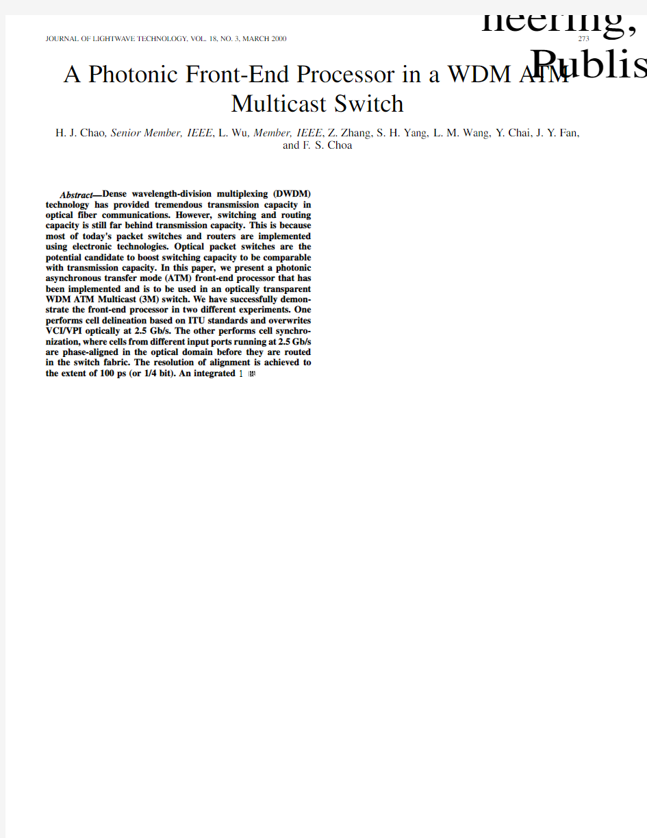
Fig.1.Architecture of the WDM ATM multicast (3M)
Switch.
Fig.2.Cell format adopted in the system.
also been proposed to identify packet boundaries for IP over WDM [9].Once cell boundaries are identified,the VPI/VCI and header error control (HEC)fields are replaced optically with the new values by the VCI-overwrite unit.These two units have been implemented and demonstrated at the data rate of 2.5Gb/s.
The cell synchronization unit is used to align the phases of in-coming ATM cells in the optical domain.The synchronization issue is also addressed in [19].Zucchelli and Burzio have imple-mented a two-stage cell synchronizer [10],[11],coarse and fine synchronizer,at the rate of 622Mb/s.The former uses a few
slow
thermooptic
switches to control the cells through different fiber delay lines.The latter uses a tunable wavelength converter to convert the wavelength of the cells to finely adjust the delay along a highly dispersive fiber.In our design,we adjust the phases of optical cells at 2.5Gb/s to a reference cell clock with the adjustment range from 1to 511bits and with a precision of 1/4bit (or 100ps).We have adopted a novel sampling method to achieve 100-ps precision without using a 10-GHz clock.In this paper,Section II presents an overview of the enhanced 3M switch and the optical random access memory.Section III describes the architecture of the photonic ATM front-end pro-cessor.Section IV shows the implementation and testing results.Section V presents the conclusions.
II.A N O VERVIEW OF THE 3M S WITCH
Fig.1shows the architecture of an
enhanced 3M switch,where incoming cells running at 2.5Gb/s are optically split into two paths.Cells on the top path remain in the op-tical domain and are routed through the optical switch
plane.
Fig.3.An optical random access memory.
Cells on the bottom path are converted to the electronic domain,where their headers are extracted for processing (e.g.,finding the output ports for which the cells are destined and finding new VPI/VCI values to replace the old VPI/VCI values).An electronic central controller,as shown in Fig.1,performs cell delineation,VCI-overwrite,cell synchronization,and routing.The first three functions are implemented in the photonic ATM front-end processor,while the last one is handled by a route con-troller that routes cells to proper output ports.
As shown in Fig.2,the cell format adopted in our system has 64bytes with 5bytes of header,48bytes of payload,and 2guard time fields (with all ones),which are 6and 5bytes
CHAO et al.:A PHOTONIC FRONT-END PROCESSOR IN A WDM ATM MULTICAST SWITCH275
Fig.4.An optical shared memory controlled by a route controller.
long,respectively.The guard times are used to accommodate
the slow switching of optical devices,such as optical tunable
filters.The lengths of the guard times between the cells,and
between the cell header and the payload were arbitrarily chosen
to demonstrate the feasibility of the technology.
The incoming optical cells are first delayed by fiber lines,
processed for their headers,and synchronized in the front-end
processor before they are sent to the switch fabric.In the
switch fabric,cells are converted to different wavelengths by
wavelength converters(WC’s)that are controlled by the route
controller,which keeps track of the available wavelengths in
the WDM optical shared memory.It is a fiber loop memory,
as shown in Fig.3,and is used to store optical cells until they
are ready to be transmitted to the next https://www.doczj.com/doc/a316049275.html,ing a3-dB
directional coupler,cells are coupled into the optical memory
and coexist with the existing cells.Accessing cells in the
optical memory is done by controlling the space switches
(SW’s),e.g.,semiconductor optical amplifier(SOA)gate.The
maximum number of cells(i.e.,wavelengths)simultaneously
stored in this memory is
output ports by a splitter and selected by the
destined output port(or ports,if multicast)through tunable
filters that are tuned by the route controller at a per-cell basis.
The final wavelength converter stage converts cells to their
predetermined wavelengths.Other optical loop memory can be
found in[20]–[22].
Fig.4shows how the shared memory is controlled by a
route controller.
276JOURNAL OF LIGHTW A VE TECHNOLOGY ,VOL.18,NO.3,MARCH
2000
Fig.6.Block diagram of the cell delineation
unit.
Fig.7.Block diagram of the VCI-overwrite unit.
The write controller and read controller generate proper signals to coordinate all functional blocks.
The jitter from the high-speed control circuits (2.5GHz)has been minimized by taking some careful steps,such as opti-mizing circuits design at 2.5GHz,using high-speed ECL and GaAs chips,Getek PCB material.
III.T HE A RCHITECTURE OF THE P HOTONIC ATM F RONT -E ND
P ROCESSOR The header of an ATM cell carries all necessary routing in-formation.The photonic ATM front-end processor is designed to extract cell headers and perform cell delineation,VCI-over-
CHAO et al.:A PHOTONIC FRONT-END PROCESSOR IN A WDM ATM MULTICAST SWITCH
277
Fig.8.Block diagram of the cell synchronization unit.
write,and cell synchronization.The front-end processor pre-sented in the paper is used for an OC-48line.The optical devices in the system need to have flat gain over wide bandwidth to ac-commodate WDM applications.The gain of the optical switches used in the system is kept just enough to overcome the insertion loss while input power is sufficiently high to suppress the ASE noise.
A.Cell Delineation Unit
As shown in Fig.1,an optical cell stream is tapped from each input line,converted to electronic format,and sent to the cell delineation unit.Cell delineation is a process used to identify cell boundaries so that the incoming cell stream can be further processed at the cell level by the following units,such as VCI-overwrite.
We adopted the standardized HEC checking mechanism to find cell boundaries.It takes advantage of the inherent Cyclic Redundancy Check(CRC)coding correlation between the cell header to be protected(the first4bytes)and HEC byte(the fifth byte of the cell header).Fig.5shows the state diagram of cell delineation.Initially,a cell boundary is arbitrarily assumed and checked by performing a polynomial division bit-by-bit in the HUNT state(Fig.5).If the remainder(i.e.,syndrome)for a com-plete calculation is zero,then this boundary is assumed to be correct.Otherwise,shift a bit from the data stream and repeat the operation until the syndrome is zero.Once a cell boundary is determined,it has to be confirmed cell-by-cell for eight con-secutive times in the PRESYNC state before the cell boundary is claimed to be found.It then goes to the SYNC state.Once in the SYNC state,the cell boundary is claimed to be lost when seven consecutive mismatches occur.As a result,the above procedure for cell delineation will start over again(from the HUNT
state).Fig.9.Block diagram of the timing signal generator.
As shown in Fig.6,to reduce the high-speed circuit require-ment,the serial bit stream at2.5Gb/s is first converted to16-bit parallel words(155Mb/s)through a serial to parallel converter. A16-bit parallel format of the CRC circuit is used to perform polynomial division and the syndrome is checked every three word clock cycles.An HPS(HUNT,PRESYNC,and SYNC)fi-nite state machine performs the state transition between HUNT, PRESYNC,and SYNC states in Fig.5.If a syndrome equals zero,then the finite state machine goes to the PRESYNC state from the HUNT state and disables a set of control and shift cir-cuits by a signal Y.Otherwise,the finite state machine informs the control and shift circuits to inhibit a bit or a byte every three cell clock cycles.Once the cell boundary is confirmed,the state machine goes to the SYNC state and sends a signal X to create a cell clock,which indicates the location of the cell boundary.The cell clock and signal X are passed to the VCI-overwrite unit to-gether with the old VPI/VCI and the word clock.In our design, the cell boundary can be identified within72cell time slots from a random bit stream.
Identifying cell boundaries for a back-to-back cell stream at 2.5Gb/s without using SONET frames is much more difficult than the case where cells are carried over SONET frames.In our design,when an error HEC is detected in the HUNT state,
278JOURNAL OF LIGHTW A VE TECHNOLOGY ,VOL.18,NO.3,MARCH
2000
Fig.10.Sample timing of the fine adjustment circuit (1=4
bit).
Fig.11.Fine delay comparator.
the system clock (2.5GHz)is shifted by one bit to restart the HEC hunting process as opposed to shifting one byte in the case where cells are carried over SONET frames.This is achieved by masking a clock pulse at 2.5GHz (or 200ps),which is very challenging.
B.VCI-Overwrite Unit
Once cell boundaries are recognized and confirmed by the cell delineation unit,the state machine moves to the SYNC state
and enables the VCI-overwrite unit with the cell clock and signal X,as shown in Fig.7.The main function of this unit is to over-write the VPI/VCI field of the incoming cell header in the op-tical domain.The VCI-overwrite unit performs table lookups in the electronic domain,converts the new VPI/VCI to an op-tical signal,and replaces the old VPI/VCI by using
a op-tical switch.The routing table (i.e.,VCI/VPI translation table)is pre-programmed manually for permanent virtual connections (PVC’s)and not by UNI and PNNI signaling protocols that are used for switched virtual connections (SVC’s).The challenge is how to handle the high-speed overwriting at the bit rate of 2.5Gb/s with each bit only 400ps.We resolve it by (a)replacing the whole cell header instead of just the VPI/VCI fields,and (b)using electronic variable delay lines (programmable delay)to compensate for the time difference between the old header and the new header.
As shown in Fig.7,the new header obtained from the table lookup is converted to a serial format by a parallel to serial con-verter.It is then used to control a laser driver to drive a DFB laser diode that generates the cell header in the optical domain.
The new header replaces the old one using
a
optical switch that is controlled by a 6-byte wide pulse in every cell time slot.
CHAO et al.:A PHOTONIC FRONT-END PROCESSOR IN A WDM ATM MULTICAST SWITCH 279
TABLE I
C ONVERSION T ABLE B ETWEEN [D0,D1,
D2,D3]AND [C10,
C11]
Fig.12.The PCB’s of the cell delineation and VCI-overwrite
units.
Fig.13.A portion of the PCB of the cell synchronization unit.
TABLE II
S UMMARY OF THE P RINTED C IRCUIT B
OARDS
The successfully overwritten cells are sent to fiber delay lines in the cell synchronization unit.
The switching speed of
the optical switch is 1GHz,which is sufficiently fast for our application.The time delay of the VCI-overwrite Unit is mainly caused by the VPI/VCI table lookup and is negligible as compared to the propagation delay between switch nodes.C.Cell Synchronization Unit
In the 3M switch,synchronization is done at two levels.The cell contention resolution,VCI/VPI overwrite and cell read/write from/to the loop memory are executed at the cell level while the interaction between electronic and optical signals is at the bit level.For instance,cell header overwrite optically is done at the bit level.Furthermore,synchronization among the incoming optical cells is achieved at 1/4bit.
The cell synchronization unit in Fig.8is used to optically align cells from different inputs to the extent
of
(where
280JOURNAL OF LIGHTW A VE TECHNOLOGY,VOL.18,NO.3,MARCH2000
Fig.14.A fabricated122SOA gates switch.
Fig.15.Switching characteristics of an SOA switch(200ps/div.).
Fig.16.Testing setup of the cell delineation and the VCI-overwrite units.
100ps,the phase adjustment error is limited to100ps.Table I
shows the mapping of the fine sampled value(D0–D3)to the
last two bits of the delay line control(C10,C11).
With different combinations of C1to C11,the optical delay
elements are tuned to insert the desired delay needed to align the
phase of incoming cells.For example,with[C1,C2,
[1,0,1,0,0,0,0,0,0,0,1],a total delay of
(the last term is
CHAO et al.:A PHOTONIC FRONT-END PROCESSOR IN A WDM ATM MULTICAST SWITCH 281
bit stream to 16-bit parallel words at 155Mb/s,reducing the number of high-speed components and implementation costs.A number of EPROM chips are used for VCI translation in the VCI-overwrite PCB.A 16-bit multiplexer performs parallel-to-serial conversion for the cell headers and overwrites the old VCI optically.In the cell synchronization PCB,several programmable delay chips are used to adjust the phase of some signals in the coarse and fine adjustment circuits.The delay adjustment range varies from 1390to 3630ps with approximate 20-ps delay step resolution.
Fig.12is a photograph of the cell delineation and VCI-over-write PCB’s.Fig.13shows a portion of the cell synchroniza-tion PCB.Table II summarizes the characteristics of these three PCB’s.
B.
SOA Switches
We have developed the
integrated
Y-junction SOA switches that are used in optical delay elements of the cell syn-chronization unit and the WDM optical shared memory.
Fig.14shows our
integrated
Y-junction SOA photonic switch that
is
mm.It can be fabricated on an InP sub-strate by wet etching and regrowth processing.The Y-junction passive waveguide,with a stripe width of
3.75
m.The
total length of the passive waveguide is
1200
m.They are made of InGaAs–InGaAsP
multiple quantum well around 1550nm.After the antireflec-tion coating,the ripple in the spontaneous emission spectrum is smaller than 0.2dB at the working bias current.
Fig.15shows the switching characteristics of the fabricated SOA switches.An optical “dc”signal is switched on and off by the SOA gates controlled by external electrical signals.Both the rising and falling times are around 600ps,which is par-tially limited by the driving electronics.Further improvement of the speed by reducing the area of the electrical contact 5to 10times is possible.However,since guard times between cells are employed,the subnanosecond switching speed of the de-vice is good enough for our applications.By using the fabri-
cated
SOA switch,we have demonstrated the data-block switching operation.
C.Testing of the Cell Delineation and VCI-Overwrite Units Testing is divided into two parts,one demonstrating cell de-lineation and VCI-overwrite,and the other demonstrating cell synchronization.
We integrate two PCB’s (cell delineation and VCI-overwrite units)with the necessary optical devices as shown in Fig.16.A data generator generates the 2.5-GHz Bit_clk and a series of 2.5-Gb/s back-to-back cells.To simplify the test,the gener-ated cells with the format shown in Fig.2have a random pay-load but an identical cell header pattern,which is {00001010,11001100,11101110,11110000,10100000}.We assume that only the third byte (representing VCI)and the fifth byte (HEC byte)are updated in the VCI-overwrite
unit.
Fig.17.Testing result of the cell delineation and VCI-overwrite units (3.6
ns/div).
Fig.18.Coarse delays adjustment.
Since inputs and outputs of two PCB’s have standard ECL
voltage levels,
with
V ,which is different from that of the laser driver
(
V),an amplifier is needed.
The optical switch is accomplished by two modulators and drivers that are controlled by the VCI-overwrite unit.A high-speed os-cilloscope is used to examine the overwritten cell stream,which is converted from optical format to electronic format by an O/E converter.
When the system is powered on,the data generator provides a cell stream and a Bit_clk to the system.Depending on the position of the first cell boundary selected by the cell delineation unit,the correct updated cells can be obtained and monitored in the oscilloscope.
Fig.17shows the testing results of the cell delineation and VCI-overwrite units.The new header becomes {00001010,11001100,00010001,11110000,01110111},which meets our expectation.
D.Testing of the Cell Synchronization Unit
The cell synchronizer PCB controls the 11stages of optical delay elements through C1to C11signals that turn on or off
the
Y-junction SOA switches.The fiber delay length varies
from
to is the number of delay stages.Fig.18illustrates
the
282JOURNAL OF LIGHTW A VE TECHNOLOGY,VOL.18,NO.3,MARCH2000
Fig.19.Testing setup of the cell synchronization unit.
Fig.20.Fine delay adjustments(200ps/div).
The testing setup shown in Fig.19generates three cell
streams at2.5Gb/s through Routes1,2,and3.To simplify
the testing,instead of using the Cell_clk derived from the cell
delineation unit,we use the Cell_clk from the data generator
with a frequency of of the bit clock(2.5GHz).Since the
most challenging part of the experiment is to adjust the phase
of the incoming cells to the neighborhood of one bit,we only
control the last three stages of the delay elements,while the
first eight stages are replaced by a fiber line(Delay2)with a
delay of510bits.In our setup,we let the Ref_clk synchronize
with the Cell_clk.By varying the length of fiber delay line
(Delay1),the phase of the cell stream is set to
1010(64bytes),has
been shown to delay by511
CHAO et al.:A PHOTONIC FRONT-END PROCESSOR IN A WDM ATM MULTICAST SWITCH
283
Fig.22.X-axis:time,2ns/div;Y-axis:relevant voltage.A partial PRBS pattern of a cell operating at 2.5Gb/s and circulating up to 23loops with the wavelength of 1556.5
nm.
Fig.23.X-axis:wavelength;Y-axis:relevant power.The optical spectrum of the two WDM cells operating at 2.5Gb/s.
and the number of circulations of the ATM cell in the loop memory.
The testing setup is shown in Fig.21.Four bit streams are generated from the Pattern Generator and carried by four different wavelengths.At the rate of 2.5Gb/s,each consists of a 64-byte cell followed by a string of zero bits.The cell is generated according to pseudorandom binary sequence (PRBS)and its duration (t2)is 205ns.These four wave-lengths are multiplexed by a 4-to-1multiplexer.Through a coupler,50%of the power is fed to the loop memory and the other 50%is used for monitoring.The waveguide grating router (WGR)splits the multiplexed wavelengths into four separate paths,each passing a polarization controller (PC),optical switch (SW),and attenuator.The erbium-doped fiber amplifier (EDFA)is used to compensate for the power loss due to multiple circulations in the loop memory.The four optical switches are controlled by the FPGA chip with S1–S4signals according to the operation modes,e.g.,writing cells
into the loop memory,reading cells from the loop memory,and circulating cells in the loop memory.Fig.21(b)shows one of the input bit streams,D1.Two cells carried
by
generated from the Pattern Generator.CLOCK is an external clock signal to the FPGA controller,which is independent from
the bit streams
.The duration of the S1signal (t4and t5)corresponds to the write and read cycles,respectively,as does t6and t7in the S2signal.The duration can be adjusted flexibly by the FPGA chip and the adjustment precision is 9ns.The guard time,t3,is 13%–20%of t2.
Fig.22shows a partial PRBS pattern of a cell operating at 2.5Gb/s and circulating up to 23loops with the wavelength of 1556.5nm.Fig.23shows the optical spectrum of two WDM cells operating at 2.5Gb/s,and their corresponding wavelengths
(
Y-junction
SOA switch has been developed and used as the space switch in the cell synchronizer and the WDM loop memory.
284JOURNAL OF LIGHTW A VE TECHNOLOGY,VOL.18,NO.3,MARCH2000
The WDM loop memory has been demonstrated to be able to store two WDM cells and circulate them up to23turns at2.5 Gb/s.A dynamic refresh controller for multiple WDM channels in the loop memory is being designed with FPGA chips.
R EFERENCES
[1]N.V.Srinivasan,“Add-drop multiplexers and cross-connects for multi-
wavelength optical networking,”in Tech.Dig.,OFC'98,San Jose,CA, 1998,pp.57–58.
[2] C.K.Chan,F.Tong,L.K.Chen,and K.W.Cheung,“Demonstration of
an add-drop network node with time slot access for high-speed WDMA dual bus/ring packet networks,”in Tech.Dig.,OFC'98,San Jose,CA, 1998,pp.62–64.
[3]G.Chang,G.Ellinas,J.K.Gamelin,M.Z.Iqbal,and C.A.Brackett,
“Multiwavelength reconfigurable WDM/ATM/SONET network testbed,”J.Lightwave Technol.,vol.14,pp.1320–1340,1996.
[4]R.E.Wanger,R.C.Alferness,A.A.M.Saleh,and M.S.Goodman,
“MONET:Multiwavelength optical networking,”J.Lightwave Technol., vol.14,pp.1349–1355,1996.
[5]S.Okamoto and K.Sato,“Optical path cross-connect systems for pho-
tonic transport networks,”in Proc.IEEE Global Telecommun.Conf., 1993,pp.474–480.
[6] A.K.Srivastava,Y.Sun,J.W.Sulhoff,C.Wolf,M.Zirngibl,R.Mon-
nard,A.R.Chraplyvy,A.A.Abramov,R.P.Espindola,T.A.Strasser, J.R.Pedrazzani,A.M.Vengsarkar,J.L.Zyskind,J.Zhou,D.A.Fer-rand,P.F.Wysocki,J.B.Judkins,S.W.Granlund,and Y.P.Li,“1Tb/s transmission of100WDM10Gb/s channels over400km of Truewave?fiber,”in Proc.OFC'98,San Jose,CA,1998,PD10-1-4.
[7] F.S.Choa and H.J.Chao,“On the optically transparent WDM ATM
multicast(3M)switches,”Fiber Integr.Opt.,vol.15,pp.109–123,1996.
[8]Y.Chai,J.H.Chen,F.S.Choa,J.P.Zhang,J.Y.Fan,and W.Lin,
“Scalable and modularized optical random access memories for optical packet switching networks,”in Proc.CLEO'98,,1998,CThO17.
[9]J.Carlson,J.Manchester,and https://www.doczj.com/doc/a316049275.html,ngner,PPP over simple data link
(SDL)Using SONET/SDH with ATM-like framing,Nov.6,1998.In-ternet-Draft.
[10]M.Burzio,P.Cinato,R.Finotti,P.Gambini,M.Puleo,E.Vezzoni,and
L.Zucchelli,“Optical cell synchronization in an ATM optical switch,”
in Proc.ECOC'94,Firenze,Italy,1994,pp.581–584.
[11]L.Zucchelli,M.Burzio,and P.Gambini,“New solution for optical
packet delineation and synchronization in optical packet switched networks,”in Proc.ECOC'96,Oslo,Norway,1996,pp.301–304. [12]Y.Chai,J.H.Chen,X.J.Zhao,J.P.Zhang,J.Y.Fan,F.S.Choa,and
W.Lin,“Optical DRAM’s using refreshable WDM loop memories,”in Proc.ECOC'98,Madrid,Spain,1998.
[13]H.J.Chao,Z.Zhang,L.Wu,S.Yang,F.S.Choa,and L.Wang,“A
photonic ATM front-end processor,”in Proc.IEEE LEOS'98,Orlando, FL,Dec.1–4,1998,pp.287–288.
[14]H.J.Chao,L.Wu,Z.Zhang,S.H.Yang,L.M.Wang,Y.Chai,J.Y.
Fan,J.P.Zhang,and F.S.Choa,“A2.5Gbit/s optical ATM cell synchro-nizer,”in Proc.OFC'99,San Diego,CA,Feb.21–26,1999,pp.347–349.
[15]M.Guizani,“Simulation and logic design of optical ATM switch,”in
Proc.1997Summer Comput.Simulation Conf.Simulation and Mod-eling Technol.Twenty-First Century,San Diego,CA,1997,pp.203–208.
SCSI.
[16] D.K.Hunter,“Switch with large optical buffers(SLOB)for ATM
traffic,”Proc.SPIE,vol.2919,pp.11–18,1996.
[17]M.Tsukada,D.Z.Wen,T.Matsunaga,M.Asobe,and T.Oohara,“An
ultrafast photonic ATM switch based on bit-interleave multiplexing,”J.
Lightwave Technol.,vol.14,pp.1979–1985,Sept.1996.
[18]M.Guizani and A.M.Memon,“SEROS:A self-routing optical ATM
switch,”https://www.doczj.com/doc/a316049275.html,mun.Syst.,vol.9,no.2,pp.115–125,Mar.–Apr.
1996.
[19]Y.Takahashi,K.Ando,M.Miyata,and E.Amada,“New retiming and
synchronization scheme for optical ATM switching systems,”Electron.
Lett.,vol.26,no.2,pp.99–100,Jan.18,1990.
[20]https://www.doczj.com/doc/a316049275.html,ngenhorst et al.,“Fiber loop optical buffer,”J.Lightwave Technol.,
vol.14,pp.324–335,Mar.1996.
[21]G.Bendelli et al.,“Photonic ATM switch based on a multiwavelength
fiber-loop buffer,”in Proc.OFC'95,Paper WJ4,pp.141–142.
[22]Y.Yamada et al.,“Transparent optical-loop memory for optical FDM
packet buffering with differential receiver,”in Proc.ECOC'96,Sept.
15–19,1996,pp.
317–320.
H.J.Chao(S’82–M’85–SM’95)received the
B.S.E.E.and M.S.E.E.degrees from the National
Chiao-Tung University,Taiwan,R.O.C.,in1977
and1980,respectively.He received the Ph.D.
degree in electrical engineering from The Ohio State
University,Columbus,in1985.
He is Professor of the Department of Electrical
Engineering at Polytechnic University,Brooklyn,
NY,which he joined in January1992.His research
interests include terabit IP routers,optical packet
switches,and quality of service control in IP/ATM networks.From1985to1991,he was a Member of Technical Staff at Bellcore, NJ,where he conducted research in the area of SONET/ATM broad-band networks.He was involved in architecture designs and ASIC implementations, such as the first SONET-like Framer chip,ATM Layer chip,and Sequencer chip(the first chip handling packet scheduling).
Dr.Chao received the Bellcore Excellence Award in1987.He served as Guest Editor for the IEEE J OURNAL ON S ELECTED A REAS IN C OMMUNICATIONS (JSAC)with special topics on“Advances in ATM Switching Systems for B-ISDN”(June1997)and“Next Generation IP Switches and Routers”(June 1999).He is currently serving as an Editor for the IEEE/ACM T RANSACTIONS ON N ETWORKING
.
L.Wu(M’97)received the B.S.,M.S.,and Ph.D.de-
grees in electronic engineering from Tsinghua Uni-
versity,Beijing,China,in1988,1991,and1997,re-
spectively.
He was a Senior Lecturer in the Department
of Electronic Engineering,Tsinghua University
from1994to early1997.After his research and
development work on multimedia DSP chips in
1997,he joined the Center for Advanced Technology
in Telecommunications,the Department of Electrical
Engineering,Polytechnic University,Brooklyn,NY, as a Postdoctoral Fellow,working on design and implementation of high-speed digital control circuits and systems utilized in WDM ATM Multicast optical switching systems.He is also working on ASIC design of the ATM switch chips.His current interest is on high-speed digital circuits and systems utilized in optical fiber communications and ASIC design of ATM switch chips and DSP chips.
Dr.Wu received the Tsinghua University Excellence Graduate Award and Medal in
1988.
Z.Zhang was born in Liaoning,China,in1967.He
received the B.Sc.degree in electronic engineering
and the Ph.D.degree in opto-electronics from
Tsinghua University,China,in1989and1996,
respectively.
During1996,he was with the Department of
Electronic Engineering at Tsinghua University,
working on optical time-division and wavelength-di-
vision multiplexed ATM switching system.From
late1996to1998,he was a postdoctoral Fellow
with the Department of Electrical Engineering at the Polytechnic University,Brooklyn,NY,working on photonic ATM front-end processor and3M(WDM,A TM,Multicast)optical switching system.Since early1999,he has been a Hardware Design Engineer at Fujitsu Network Communications,Inc.,Pearl River,NY,working on ATM switching systems. His research interests are in ATM network,photonic packet switching and optical WDM
network.
S.H.Yang received the B.S.degree in physics from
Soochow University,Taiwan,R.O.C.,in1987,the
M.S.degree in electro/optical engineering from the
National Chiao-Tung University,Taiwan,in1989,
and the Ph.D.degree in electrical engineering from
Polytechnic University,Brooklyn,NY,in1999.
In1999,he joined the Transcomm Technology
System,Inc.,Fremont,CA,where he works in the
area of access networks.His research interests are
in the area of ATM switches,IP routers,and access
network systems.
CHAO et al.:A PHOTONIC FRONT-END PROCESSOR IN A WDM ATM MULTICAST SWITCH 285
L.M.Wang received the B.S.degree in physics and the M.S.degree in Optics from the University of Electronic Science and Technology of China,Chengdu,Sichuan,China,in 1985and 1991,respectively.He received a second M.S.de-gree in physics from Indiana University–Purdue University at Indianapolis,IN,in 1996.He received the Ph.D.degree in electrical engineering from the Uni-versity of Maryland Baltimore County (UMBC),Baltimore,MD,in May 1999.From July 1996to May 1999,he worked on the opto-electronic devices and their applications in optical access networks and all-optical packet switches.He joined Corning,Inc.,Corning,NY ,in May 1999,as Senior Scientist in fiber communications.His current interests are dispersion-managed fibers and soliton
transmissions.Y.Chai received the B.S.,M.S.,and Ph.D.degrees in electrical engineering from Tsinghua University,Beijing,China,in 1986,1988,and 1992,respectively.He was a Lecturer and an Associate Professor in the Department of Electronic Engineering,Tsinghua University,Beijing,China,from 1992to 1996.He joined the faculty of the Department of Computer Science and Electrical Engineering,University of Maryland Baltimore County (UMBC),Baltimore,MD,as a Research Associate from 1996to 1999.He is now with Tyco Submarine
Systems,Ltd.,Eatontown,NJ.He worked on tunable semiconductor lasers,laser frequency stabilization,optical FDM transmission,high-speed WDM transmission system,and optical packet switching networks.He has more than 60publications and presentations,and holds two patents.His current interest is on undersea optical WDM transmission systems and gain-flattened broad-band
EDFA.
J.Y.Fan received the B.S.degree in physics from the National Tsinghua University,Taiwan,R.O.C.,in 1988,the M.S.degree in electro-optical engineering from the National Chiao-Tung University,Taiwan,in 1990and the Ph.D.degree in electrical engineering from the University of Maryland Baltimore County (UMBC),Baltimore,MD,in 1999.His Ph.D.work concentrated on the design,fabrication,and implementation of high-speed photonic switching in a photonic IP/ATM system and demultiplexing/mul-tiplexing for TDM system,and wavelength converts
for WDM system.
He is now with Nanovation Technologies,Inc.,Evanston,IL,where he is doing research work in thin-film photonic devices for optical communications.
F.S.Choa received the B.S.degree from the National Taiwan University,Taiwan,R.O.C.,and the M.S.and Ph.D.degrees from the State University of New York (SUNY)at Buffalo,NY .
After his Ph.D.research work on femtosecond infrared lasers and detectors in 1988,he joined AT&T Bell Laboratories,in Holmdel and Murray Hill,NJ,where he worked in the area of photonic integrated circuits and chemical beam epitaxy.Since joining the University of Maryland Baltimore County (UMBC),Baltimore,MD,he has been working in the areas of III–V compound semi-conductor material growth and processing,RF-photonic devices and systems,photonic IP/ATM switching,ultrahigh capacity WDM communications and net-works,and fiber-optic sensors for biomedical sensing.He has authored and coauthored more than 130refereed journal and conference publications.
Dr.Choa is a Topical Editor for Optics Letters and Associate Editor of the Journal of High-Speed Networks .
play a part (in) 重要程度:★☆☆☆☆难易程度:★★☆☆☆ Have you realized the part computers have ___________ in the daily life? A. made B. given C. caused D. played 【参考答案】D 【拓展延伸】 1. play a part (in) 在……中扮演一个角色;参与;在……中起作用 2. play the role of 扮演……的角色 play an important role / part in...在……中起重要作用 play the leading role / part主演;起带头作用 3. take part in 参加 for the most part多半;在很大程度上 for one’s part就某人而言,对某人来说 1. Colors play an important ___________ in the way you look. A. part B. form C. effect D. pride 2. Mr. Huang will ___________ in the movement. A. play a leading part B. take parts C. play leading part D. take a part 3. __________ part that women ___________ in society is great. A. The; plays B. A; takes C. A; plays
【摘要】黄自先生是我国杰出的音乐家,他以艺术歌曲的创作最为代表。而黄自先生特别强调了钢琴伴奏对于艺术歌曲组成的重要性。本文是以黄自先生创作的具有爱国主义和人道主义的艺术歌曲《天伦歌》为研究对象,通过对作品分析,归纳钢琴伴奏的弹奏方法与特点,并总结黄自先生的艺术成就与贡献。 【关键词】艺术歌曲;和声;伴奏织体;弹奏技巧 一、黄自艺术歌曲《天伦歌》的分析 (一)《天伦歌》的人文及创作背景。黄自的艺术歌曲《天伦歌》是一首具有教育意义和人道主义精神的作品。同时,它也具有民族性的特点。这首作品是根据联华公司的影片《天伦》而创作的主题曲,也是我国近代音乐史上第一首为电影谱写的艺术歌曲。作品创作于我国政治动荡、经济不稳定的30年代,这个时期,这种文化思潮冲击着我国各个领域,连音乐艺术领域也未幸免――以《毛毛雨》为代表的黄色歌曲流传广泛,对人民大众,尤其是青少年的不良影响极其深刻,黄自为此担忧,创作了大量艺术修养和文化水平较高的艺术歌曲。《天伦歌》就是在这样的历史背景下创作的,作品以孤儿失去亲人的苦痛为起点,发展到人民的发愤图强,最后升华到博爱、奋起的民族志向,对青少年的爱国主义教育有着重要的影响。 (二)《天伦歌》曲式与和声。《天伦歌》是并列三部曲式,为a+b+c,最后扩充并达到全曲的高潮。作品中引子和coda所使用的音乐材料相同,前后呼应,合头合尾。这首艺术歌曲结构规整,乐句进行的较为清晰,所使用的节拍韵律符合歌词的特点,如三连音紧密连接,为突出歌词中号召的力量等。 和声上,充分体现了中西方作曲技法融合的创作特性。使用了很多七和弦。其中,一部分是西方的和声,一部分是将我国传统的五声调式中的五个音纵向的结合,构成五声性和弦。与前两首作品相比,《天伦歌》的民族性因素增强,这也与它本身的歌词内容和要弘扬的爱国主义精神相对应。 (三)《天伦歌》的伴奏织体分析。《天伦歌》的前奏使用了a段进唱的旋律发展而来的,具有五声调性特点,增添了民族性的色彩。在作品的第10小节转调入近关系调,调性的转换使歌曲增添抒情的情绪。这时的伴奏加强和弦力度,采用切分节奏,节拍重音突出,与a段形成强弱的明显对比,突出悲壮情绪。 c段的伴奏采用进行曲的风格,右手以和弦为主,表现铿锵有力的进行。右手为上行进行,把全曲推向最高潮。左手仍以柱式和弦为主,保持节奏稳定。在作品的扩展乐段,左手的节拍低音上行与右手的八度和弦与音程对应,推动音乐朝向宏伟、壮丽的方向进行。coda 处,与引子材料相同,首尾呼应。 二、《天伦歌》实践研究 《天伦歌》是具有很强民族性因素的作品。所谓民族性,体现在所使用的五声性和声、传统歌词韵律以及歌曲段落发展等方面上。 作品的整个发展过程可以用伤感――悲壮――兴奋――宏达四个过程来表述。在钢琴伴奏弹奏的时候,要以演唱者的歌唱状态为中心,选择合适的伴奏音量、音色和音质来配合,做到对演唱者的演唱同步,并起到连接、补充、修饰等辅助作用。 作品分为三段,即a+b+c+扩充段落。第一段以五声音阶的进行为主,表现儿童失去父母的悲伤和痛苦,前奏进入时要弹奏的使用稍凄楚的音色,左手低音重复进行,在弹奏完第一个低音后,要迅速的找到下一个跨音区的音符;右手弹奏的要有棱角,在前奏结束的时候第四小节的t方向的延音处,要给演唱者留有准备。演唱者进入后,左手整体的踏板使用的要连贯。随着作品发展,伴奏与旋律声部出现轮唱的形式,要弹奏的流动性强,稍突出一些。后以mf力度出现的具有转调性质的琶音奏法,要弹奏的如流水般连贯。在重复段落,即“小
我国艺术歌曲钢琴伴奏-精 2020-12-12 【关键字】传统、作风、整体、现代、快速、统一、发展、建立、了解、研究、特点、突出、关键、内涵、情绪、力量、地位、需要、氛围、重点、需求、特色、作用、结构、关系、增强、塑造、借鉴、把握、形成、丰富、满足、帮助、发挥、提高、内心 【摘要】艺术歌曲中,伴奏、旋律、诗歌三者是不可分割的重 要因素,它们三个共同构成一个统一体,伴奏声部与声乐演唱处于 同样的重要地位。形成了人声与器乐的巧妙的结合,即钢琴和歌唱 的二重奏。钢琴部分的音乐使歌曲紧密的联系起来,组成形象变化 丰富而且不中断的套曲,把音乐表达的淋漓尽致。 【关键词】艺术歌曲;钢琴伴奏;中国艺术歌曲 艺术歌曲中,钢琴伴奏不是简单、辅助的衬托,而是根据音乐 作品的内容为表现音乐形象的需要来进行创作的重要部分。准确了 解钢琴伴奏与艺术歌曲之间的关系,深层次地了解其钢琴伴奏的风 格特点,能帮助我们更为准确地把握钢琴伴奏在艺术歌曲中的作用 和地位,从而在演奏实践中为歌曲的演唱起到更好的烘托作用。 一、中国艺术歌曲与钢琴伴奏 “中西结合”是中国艺术歌曲中钢琴伴奏的主要特征之一,作 曲家们将西洋作曲技法同中国的传统文化相结合,从开始的借鉴古 典乐派和浪漫主义时期的创作风格,到尝试接近民族乐派及印象主 义乐派的风格,在融入中国风格的钢琴伴奏写作,都是对中国艺术 歌曲中钢琴写作技法的进一步尝试和提高。也为后来的艺术歌曲写 作提供了更多宝贵的经验,在长期发展中,我国艺术歌曲的钢琴伴 奏也逐渐呈现出多姿多彩的音乐风格和特色。中国艺术歌曲的钢琴
写作中,不可忽略的是钢琴伴奏织体的作用,因此作曲家们通常都以丰富的伴奏织体来烘托歌曲的意境,铺垫音乐背景,增强音乐感染力。和声织体,复调织体都在许多作品中使用,较为常见的是综合织体。这些不同的伴奏织体的歌曲,极大限度的发挥了钢琴的艺术表现力,起到了渲染歌曲氛围,揭示内心情感,塑造歌曲背景的重要作用。钢琴伴奏成为整体乐思不可缺少的部分。优秀的钢琴伴奏织体,对发掘歌曲内涵,表现音乐形象,构架诗词与音乐之间的桥梁等方面具有很大的意义。在不断发展和探索中,也将许多伴奏织体使用得非常娴熟精确。 二、青主艺术歌曲《我住长江头》中钢琴伴奏的特点 《我住长江头》原词模仿民歌风格,抒写一个女子怀念其爱人的深情。青主以清新悠远的音乐体现了原词的意境,而又别有寄寓。歌调悠长,但有别于民间的山歌小曲;句尾经常出现下行或向上的拖腔,听起来更接近于吟哦古诗的意味,却又比吟诗更具激情。钢琴伴奏以江水般流动的音型贯穿全曲,衬托着气息宽广的歌唱,象征着绵绵不断的情思。由于运用了自然调式的旋律与和声,显得自由舒畅,富于浪漫气息,并具有民族风味。最有新意的是,歌曲突破了“卜算子”词牌双调上、下两阕一般应取平行反复结构的惯例,而把下阕单独反复了三次,并且一次比一次激动,最后在全曲的高音区以ff结束。这样的处理突出了思念之情的真切和执著,并具有单纯的情歌所没有的昂奋力量。这是因为作者当年是大革命的参加者,正被反动派通缉,才不得不以破格的音乐处理,假借古代的
play a part in的用法 Do you know this pretty girl Right! She is Audrey Hepburn who played many classic roles in a great many famous films. For example, < Roman Holiday> is the one of the films which earned Hepburn her first Academy Award for Best Actress. Audrey Hepburn played the part/role of Princess Ann in this film. play the part/role of…扮演……角色
Audrey Hepburn played a leading part in
Audrey Hepburn also played leading roles in < Funny Face>and < My Fair Lady〉.( My Fair Lady 窈窕淑女影片讲述下层卖花女被语言学教授改造成优雅贵妇的故事,从头至尾洋溢着幽默和雅趣 .Funny Face 甜姐儿) Play a role in…在……中扮演角色,在……中起作用 play a part/role in doing sth. 在做某事方面起作用,参与做某事 We can?all?play?a?role/part?in?reducing?our?dependence?on?plastic, if we started to?take some small?steps?in?our?everyday?lives?to?be
Unit 7 Will people have robots?知识 点整理 Unit7willpeoplehaverobots?知识点整理 一、词组、短语: 、oncomputers在电脑上, 2、onpaper在纸上, 3、livetobe200yearsold活到200岁, 4、freetime空闲时间, 5、indanger 在危险中, 6、ontheearth在世界上 7、playapartinsth在某方面出力/做贡献, 8、spacestation太空站, 8、lookfor寻找, 9、computerprogrammer电脑程序师, 10、inthefuture 在将来, 11、hundredsof成百上千的, 12、thesame…as与…一样, 13、overandoveragain反复, 14、getbored 无聊,
15、wakeup醒来/唤醒, 16、looklike 看起来像, 17、falldown倒下/落下 二、重要句子(语法) 、will+动词原形 将要做 2、fewer/more+可数名词复数更少/更多… 3、less/more+不可数名词 更少/更多 4、trytodosth. 尽力做某事 5、havetodosth 不得不做某事 6、agreewithsb. 同意某人的意见 7、such+名词(词组) 如此
8、playapartindoingsth 参与做某事 9、makesbdosth 让某人做某事 10、helpsbwithsth 帮助某人做某事 11、Therewillbe+主语+其他 将会有…. 12、Thereis/are+sb.+doingsth 有…正在做… 13、Itis +形容词+forsb+todosth 做某事对某人来说… 语法: whatwillthefuturebelike? citieswillbemorepolluted.Andtherewillbefewertrees. willpeopleusemoneyin100years?
人教版八年级英语上册Unit7知识点归纳整 理 Unit7illpeoplehaverobots? 短语归纳 onputer在电脑上2.onpaper在纸上3.aeup醒 livetodo200yearsold活动200岁5.freetie空闲时间indanger处于危险之中7.ontheearth在地球上 playapartinsth.参与某事9.inthefuture在未 0spacestation太空站11.puterprograer电脑编程员 loofor寻找13.hundredsof许多;成百上千 thesae…as…与……一样15.getbored感到厌烦的 overandoveragain多次;反复地17.falldon倒塌 ill+动词原形将要做…… feer/ore+可数名词复数更少/更多…… 0.less/ore+不可数名词更少/更多…… 1.havetodosth.不得不做某事 2.agreeithsb.同意某人的意见 3.such+名词如此…… playapartindoingsth.参与做某事 Thereillbe+主语+其他将会有…… Thereis/are+sb./sth.+doingsth.有……正在做某事
aesb.dosth.helpsb.ithsth.帮助某人做某事 trytodosth.尽力做某事 It’s+ad+forsb.todosth.对某人来说,做某事……的。 语法讲解 Boosillonlybeonputers,notonpaper.书将只在电脑里,而不是在纸上。 Thereillbeorepollution.将会有更多的污染。 ).Thereillbe+n=Thereis/aregoingtobe+n将会有…ThereisgoingtobeafootballatchthisFriday. ).pollution:污染;公害pollute:污染;弄脏polluted:受污染的 Everyoneshouldplayapartinsavingtheearth.每个人应该参与挽救地球。 Todaytherearealreadyrobotsoringinfactories.现在已经有机器人在工厂里工作了。 Therebesb.doingsth.有某人正在做…Thereisabirdsinginginthetree. Theyagreeitaytaehundredsofyears.他们同意这可能花费几百年的时间。 Ittaes+时间+todosth.某人花费时间区做某事。 Ittooehalfanhourtofinishyhoeor. agreetodosth.eagreetoeetuplaterandtalthingsover
XX九年级英语上册Unit13教案(新版人教 版) 学科English年级9班级 课型fresh课时1/6媒体ataperecorder,cAI 课题Unit13e’retryingtosavetheearth!SectionA1a~1c 话题Protectingtheenvironent 功能Talaboutpollutionandenvironentalprotection 教 学 目 标 知识 技能1.Targetlanguage: e’retryingtosavetheearth. Peoplearethroinglitterintotheriver. Theriverusedtobesoclean. Everyoneshouldhelptocleanuptheriver. Graar: Presentprogressive,usedto,odalverbs ordsandexpressions;
curriculuords:litter,botto,fisheran Usefulexpressions:befullof,put…into,thro…into,cleanup,playapartin,closedon 过程 方法Accordingtodesigningsoetass,totrainstudents’listeningabilityandtotrainstudents’unicativepetence. 情感 态度Everyoneshouldeepourriversclean. 学习策略Listeningforeyords,transforinginforation. 重点TargetLanguage 难点1.Hototrainstudents’listeningability. .Hototrainstudents’unicativepetence. 教学内容及问题情境学生活动设计意图 a.TointroduceSstotheunitgoal,talaboutpollutionanden vironentalprotection. Picture: Thefourpicturesshodifferentforsofenvironentalpollut
八年级上册英语单元知识点归纳 Unit1Wheredidyougoonvacation? 短语归纳 1.goonvacation去度假 2.stayathome待在家里 3.gotothemountains去爬山 4.gotothebeach去海滩 5.visitmuseums参观博物馆 6.gotosummercamp去参加夏令营 7.quiteafew相当多 8.studyfortests为测验而学习 9.goout出去10.mostofthetime大部分时间11.haveagoodtimedoing=havefundoing=enjoyoneself玩得高兴 去购 物because+句子 查明22.goon上上下下 用法: 3.nothing 4.seem+ 13.dislikedoingsth.不喜欢做某事 14.keepdoingsth.继续做某事keepondoingsth不停做某事 15.Whynotdo.sth.=whydon’tyoudosth为什么不做……呢? 16.so+adj.+that+从句如此……以至于…… 17.tellsb.(not)todosth.告诉某人(不要)做某事 18.enough+名词,形容词+enough 19.notreally.真的没有。 20.seemtodosth似乎好像做某事 21.Byefornow!到这该说再见了。
22.Howdoyoulike…=Whatdoyouthinkof…=Whatdoyouthinkabout… Unit2Howoftendoyouexercise? 短语 1.helpwithhousework帮助做家务 2.onweekends=ontheweekend在周末 3.howoften多久 一次howsoon多久(回答in10years)4.hardlyever几乎从不 5.onceaweek每周一次twiceamonth每月两次everyday每天three/four…timesaweek每周三四…次 6.befree=beavailable有空 7.gotothemovies去看电影 https://www.doczj.com/doc/a316049275.html,etheInternet用互联网ontheInternet在网上surftheInternet 上网 9.swingdance摇摆舞10.playtennis打网球play+ 球类/棋类/中国乐器playthe+西洋乐器11.stayuplate熬夜;睡得很晚12.atleast至少atmost最多 擅长 根本firstofall 21.suchas看牙医 用法 少…? 5.主语 7.It’ 10.What Unit3I 短语 和……相同;与……一致bedifferentfrom与……不同5.careabout关心;介意takecareof=lookafter照顾6.belikeamirror像一面镜子7.themostimportant最重要的8.aslongas只要;既然 9.bringout使显现;使表现出10.getbettergrades取得更好的成绩11.reachfor伸手取12.infact 事实上;实际上13.makefriends交朋友14.one…,theother…一个…,另一个15.touchone’sheart 感动某人16.betalentedinmusic有音乐天赋 17.shareeverything分享一切18.talkabout谈论19.primaryschoolstudents小学生middleschoolstudent中学生https://www.doczj.com/doc/a316049275.html,rmation是不可数名词,一则消息:apieceofinformation 21.theEnglishstudycenter英语学习中心 用法
XX八年级英语上册第七单元导学案(人 教版) 本资料为woRD文档,请点击下载地址下载全文下载地址Unit7 willpeoplehaverobots? Period8 SectionBSelfcheck 教师复备栏或 学生笔记栏 【学习目标】 .熟练掌握本单元词汇: 2.熟练掌握本单元句型: 5) In20years,IthinkI’llbeanewspaperreporter. ontheweekend,I’lllooklesssmartbutIwillbemorecomfortable. whatwillyour…belike? 【学习重点 难点】 本单元的单词、短语、语法 【学法指导】 及时练习与巩固
【教学过程】 一、 导入(启发探究 3分钟) 对话复习: Nick:whatareyoureading,jill? jill:It’sbookaboutfuture. Nick:Soundscool.Sowhatwillthefuturebelike? jill:well,citieswillbemorecrowdedandpolluted.Therew illbefewertreesandtheenvironmentwillbeingreatdanger. Nick:Thatsoundsbad!willwehavetomovetootherplanets. jill:maybe.ButIwanttoliveontheearth. Nick:me,too.Thenwhatcanwedo? jill:wecanuselesswaterandplantsmoretrees.Everyonesh ouldplayapartinsavingtheearth. 二、自学(自主探究 6分钟) 用法:
八年级英语上册Unit7 Will people have robots?知识点归纳 课 件www.5y https://www.doczj.com/doc/a316049275.html,八年级英语上册Unit7willpeoplehaverobots?知识点归纳 八年级上Unit7willpeoplehaverobots? oncomputer在电脑上 onpaper在纸上 livetodo200yearsold活动200岁 freetime空闲时间 indanger处于危险之中 ontheearth在地球上 playapartinsth.参与某事 spacestation太空站 lookfor寻找 computerprogrammer电脑编程员 inthefuture在未来 hundredsof许多;成百上千 thesame…as…与……一样 overandoveragain多次;反复地 getbored感到厌烦的
wakeup醒来 falldown倒塌will+动词原形 将要做…… fewer/more+可数名词复数 更少/更多……less/more+不可数名词 更少/更多…… havetodosth.不得不做某事 agreewithsb.同意某人的意见 such+名词(词组) 如此…… playapartindoingsth.参与做某事 Therewillbe+主语+其他 将会有…… Thereis/are+sb./sth.+doingsth.有……正在做某事makesb.dosth.使某人做某事 helpsb.withsth.帮助某人做某事 trytodosth.尽力做某事 It’s+adj.+forsb.todosth. 对某人来说,做某事……的。 1.ThestudentsinourschoollearnEnglish computers. A.at
八年级英语上册Unit7Willpeoplehaverobots?知识点归纳puters在电脑上, 2、onpaper在纸上, 3、livetobe200yearsold活到200岁, 4、freetime空闲时间, 5、indanger在危险中, 6、ontheearth在世界上 7、playapartinsth在某方面出力/做贡献, 8、spacestation太空站, 8、lookfor寻找, 9、computerprogrammer电脑程序师, 10、inthefuture在将来, 11、hundredsof成百上千的, 12、thesame…as与…一样, 13、overandoveragain反复, 14、getbored无聊, 15、wakeup醒来/唤醒, 16、looklike看起来像, 17、falldown倒下/落下 二、重要句子(语法) 1、will+动词原形将要做
2、fewer/more+可数名词复数更少/更多… 3、less/more+不可数名词更少/更多 4、trytodosth.尽力做某事 5、havetodosth不得不做某事 6、agreewithsb.同意某人的意见 7、such+名词(词组)如此 8、playapartindoingsth参与做某事 9、makesbdosth让某人做某事 10、helpsbwithsth帮助某人做某事 11、Therewillbe+主语+其他将会有…. 12、Thereis/are+sb.+doingsth有…正在做… 13、Itis+形容词+forsb+todosth做某事对某人来说…语法: Whatwillthefuturebelike? Citieswillbemorepolluted.Andtherewillbefewertrees. Willpeopleusemoneyin100years? No,theywon’t.Everythingwillbefree. Willtherebeworldpeace? Yes,Ihopeso. Kidswillstuffyathomeoncomputers. Theywon’tgotoschool.
八上英语复习重点总结 Unit1Wheredidyougoonvacation? 单元重点: 1)一般过去时 2)不定代词的用法: a)不定代词作主语,谓语动词用单三 b)形容词修饰不定代词要放在其后 c)something一般用在肯定句中,anything一般用在否定句和疑问句中重点词组: goonvacation去度假stayathome待在家里gotothemountains去爬山gotothebeach去海滩visitmuseums参观博物馆gotosummercamp去参观夏令营quiteafew相当多 studyfor为……而学习 goout出去 mostofthetime大部分时间tastegood尝起来很好吃ofcourse当然 feellike给……的感觉/想要inthepast在过去walkaround四处走走becauseof因为onebowlof…一碗……thenextday第二天 drinktea喝茶 findout找出;查明 goon继续 takephotos照相somethingimportant重要的事upanddown上上下下 comeup出来
用法集锦: 1)buysth.forsb./buysb.sth.为某人买某物 2)taste+adj.尝起来……look+adj.看起来…… 3)nothing…but+动词原形除了……之外什么都没有 4)seem+(tobe)+adj.看起来…… 你还能想到seem的什么用法? 5)arrivein+大地点/arriveat+小地点到达某地 6)decidetodosth.决定去做某事 7)try的用法: 作动词:trydoingsth.尝试做某事/trytodosth.尽力去做某事tryone’sbesttodosth. 作名词:haveatry 8)forgetdoingsth.忘记做过某事/forgettodosth.忘记做某事 9)enjoydoingsth.喜欢做某事 10)dislikedoingsth.不喜欢做某事 11)Whynotdo.sth.?为什么不做……呢? 12)So+adj.+that+从句如此……以至于…… 13)tellsb.(not)todosth.告诉某人(不要)做某事 14)总结keep的用法 Unit2Howoftendoyouexercise? 单元重点: 1)关于how的词组 2)频率副词的位置:放在be动词、助动词、情态动词之后,实意动词之前 3)Howoften与Howman ytimes的区别? 重点词组: helpwithhousework帮助做家务onweekends/ontheweekend在周末