
UNISONIC TECHNOLOGIES CO., LTD
2SB649/A
PNP SILICON TRANSISTOR
BIPOLAR POWER GENERAL PURPOSE TRANSISTOR
APPLICATIONS
* Low frequency power amplifier complementary pair with UTC 2SB669/A
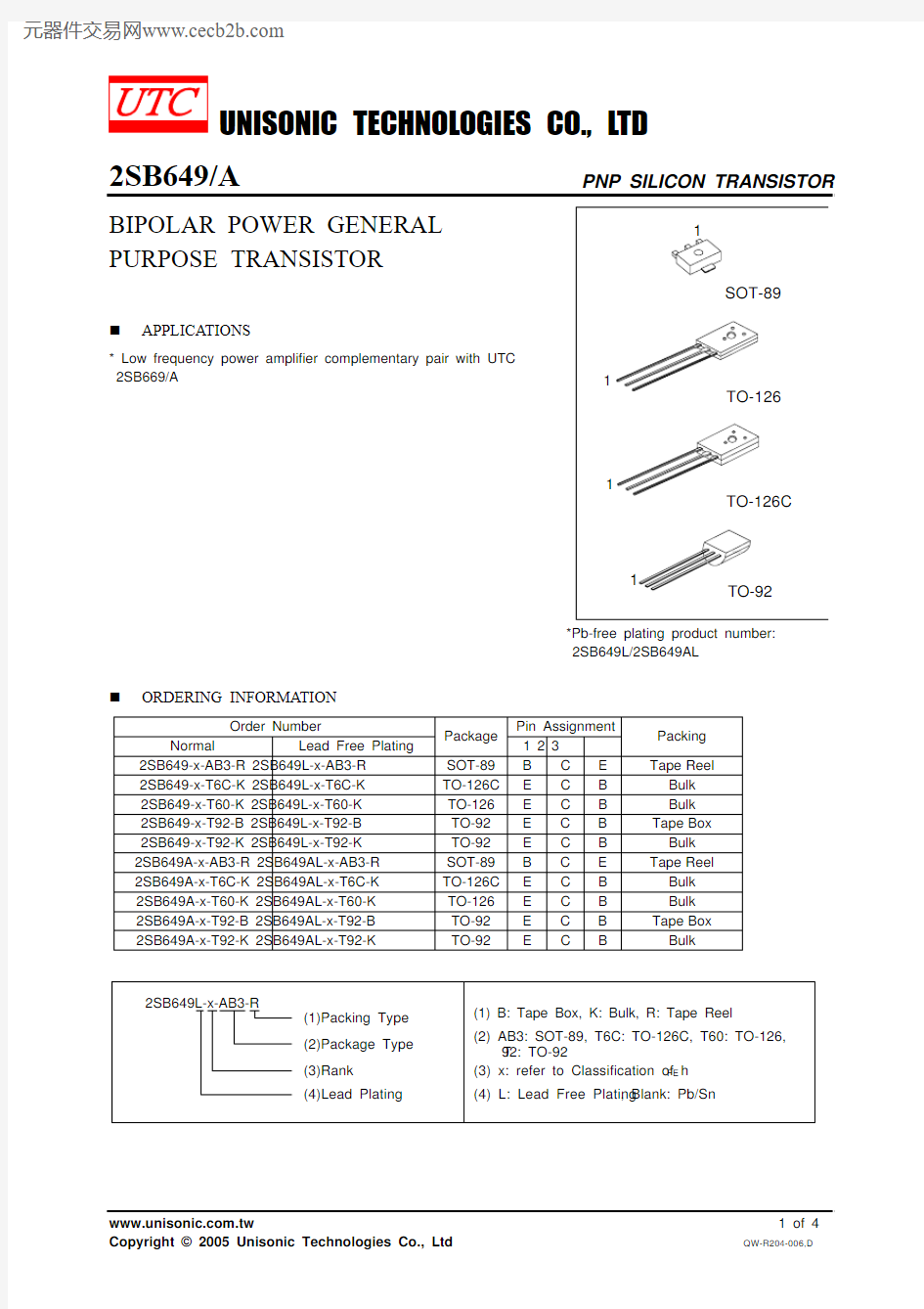
*Pb-free plating product number: 2SB649L/2SB649AL
ORDERING INFORMATION
Order Number Pin Assignment
Normal Lead Free Plating
Package 1 2 3 Packing
2SB649-x-AB3-R 2SB649L-x-AB3-R SOT-89 B C E Tape Reel 2SB649-x-T6C-K 2SB649L-x-T6C-K TO-126C E C B Bulk 2SB649-x-T60-K 2SB649L-x-T60-K TO-126 E C B Bulk 2SB649-x-T92-B 2SB649L-x-T92-B TO-92 E C B Tape Box 2SB649-x-T92-K 2SB649L-x-T92-K TO-92 E C B Bulk 2SB649A-x-AB3-R 2SB649AL-x-AB3-R SOT-89 B C E Tape Reel 2SB649A-x-T6C-K 2SB649AL-x-T6C-K TO-126C E C B Bulk 2SB649A-x-T60-K 2SB649AL-x-T60-K TO-126 E C B Bulk 2SB649A-x-T92-B 2SB649AL-x-T92-B TO-92 E C B Tape Box 2SB649A-x-T92-K 2SB649AL-x-T92-K TO-92 E C B Bulk
ABSOLUTE MAXIMUM RATING (Ta=25℃, unless otherwise specified)
PARAMETER SYMBOL RATING UNIT
Collector-Base Voltage V CBO -180 V
2SB649-120
Collector-Emitter Voltage 2SB649A V CEO -160
V
Emitter-Base Voltage V EBO -5 V Collector Current I C -1.5 A Collector Peak Current l C(PEAK)-3 A
TO-126/TO-126C 1.4 W
TO-92 1 W
Collector Power Dissipation SOT-89 P D 500 mW
Junction Temperature T J +150 °C Storage Temperature T STG -40 ~ +150 °C Note: Absolute maximum ratings are those values beyond which the device could be permanently damaged.
Absolute maximum ratings are stress ratings only and functional device operation is not implied.
ELECTRICAL CHARACTERISTICS (Ta=25℃, unless otherwise specified)
PARAMETER SYMBOL TEST CONDITIONS MIN TYP MAX UNIT
Collector to Base Breakdown Voltage BV CBO I C =-1mA, I E =0 -180 V 2SB649 -120
Collector to Emitter Breakdown Voltage 2SB649A BV CEO I C =-10mA, R BE =∞ -160 V
Emitter to Base Breakdown Voltage BV EBO I E =-1mA, I C =0 -5 V Collector Cut-off Current I CBO V CB =-160V, I E =0 -10μA
h FE1 V CE =-5V, I C =-150mA (note) 60 320
2SB649 h FE2 V CE =-5V, I C =-500mA (note) 30
h FE1 V CE =-5V, I C =-150mA (note) 60 200
DC Current Gain
2SB649A h FE2 V CE =-5V, I C =-500mA (note) 30
Collector-Emitter Saturation Voltage V CE(SAT)Ic=-600mA, I B =-50mA -1 V Base-Emitter Voltage V BE V CE =-5V, I C =-150mA -1.5V Current Gain Bandwidth Product f T V CE =-5V,I C =-150mA 140 MHz Output Capacitance Cob V CB =-10V, I E =0, f=1MHz 27 pF Note: Pulse test.
CLASSIFICATION OF h FE
RANK B C D RANGE 60-120 100-200 160-320
TYPICAL CHARACTERISTICS
0-10-20-30-40-50
0.2
0.40.60.81.0Typical Output Characteristecs Collector to Emitter Voltage, V CE (V)
C o l l e c t o r C u r r e n t , I C (A )
Base to Emitter Voltage , V BE (V)0
-0.2-0.4-0.6-0.8-1.0-1
-10
-100
-500Typical Transfer Characteristics
C o l l e c t o r C u
r r e n t ,
I C (m A )
150100150200250
300-1
-10-100-1,000Collector Current, I C (mA)D C C u r r e n t T r a n s f e r R a t i o , h F E
DC Current Transfer Ratio vs. Collector Current
Collector to Emitter Saturation Voltage
vs. Collector Current
-1-10-100
-1,000
Collector Current, I C (mA)
-0.2-0.4-0.6-0.8-1.0-1.2C o l l e c t o r t o E m i t t e r S a t u r a t i o n V o l t a g e , V C E (S A T ) (V )
350
1
310301003001,000
00.20.40.60.81.01.2Collector C urrent, I C (mA)
Base to Emitter Saturation Voltage
vs. Collector Current B a s e t o E m i t t e r S a t u r a t i o n V o l t a g e , V B E (S A T ) (V )
10
301003001,000Collector Current, I C (mA)
04080120160200240G a i n B a n d w i d t h P r o d u c t , f T (M H z )
Gain Bandwidth Product vs. Collector Current
TYPICAL CHARACTERISTICS(Cont.)
-1
-10-30-100
-325102050100200
Collector to Base Voltage, V CB (V)
Collector Output Capacitance vs. Collector to Base Voltage
C o l l e c t o r O u t p u t C a p a c i t a n c e , C o b (p F )
Area of Safe Operation
Collector to Emitter Voltage, V CE (V)
-1
-3
-10
-100-300
-0.1-0.3-1.0-3-30
C o l l e c t o r C u r r e n t
, I C (A )