Parameter
Max.
Units
V CES
Collector-to-Emitter Breakdown Voltage 600V I C @ T C = 25°C Continuous Collector Current 49I C @ T C = 100°C Continuous Collector Current 27A
I CM Pulsed Collector Current Q
200I LM Clamped Inductive Load Current R 200V GE Gate-to-Emitter Voltage
± 20V E ARV
Reverse Voltage Avalanche Energy S 15mJ P D @ T C = 25°C Maximum Power Dissipation 160P D @ T C = 100°C Maximum Power Dissipation 65
T J Operating Junction and
-55 to + 150
T STG
Storage Temperature Range
Soldering Temperature, for 10 seconds 300 (0.063 in. (1.6mm from case )
°C
Mounting torque, 6-32 or M3 screw.
10 lbf?in (1.1N?m)
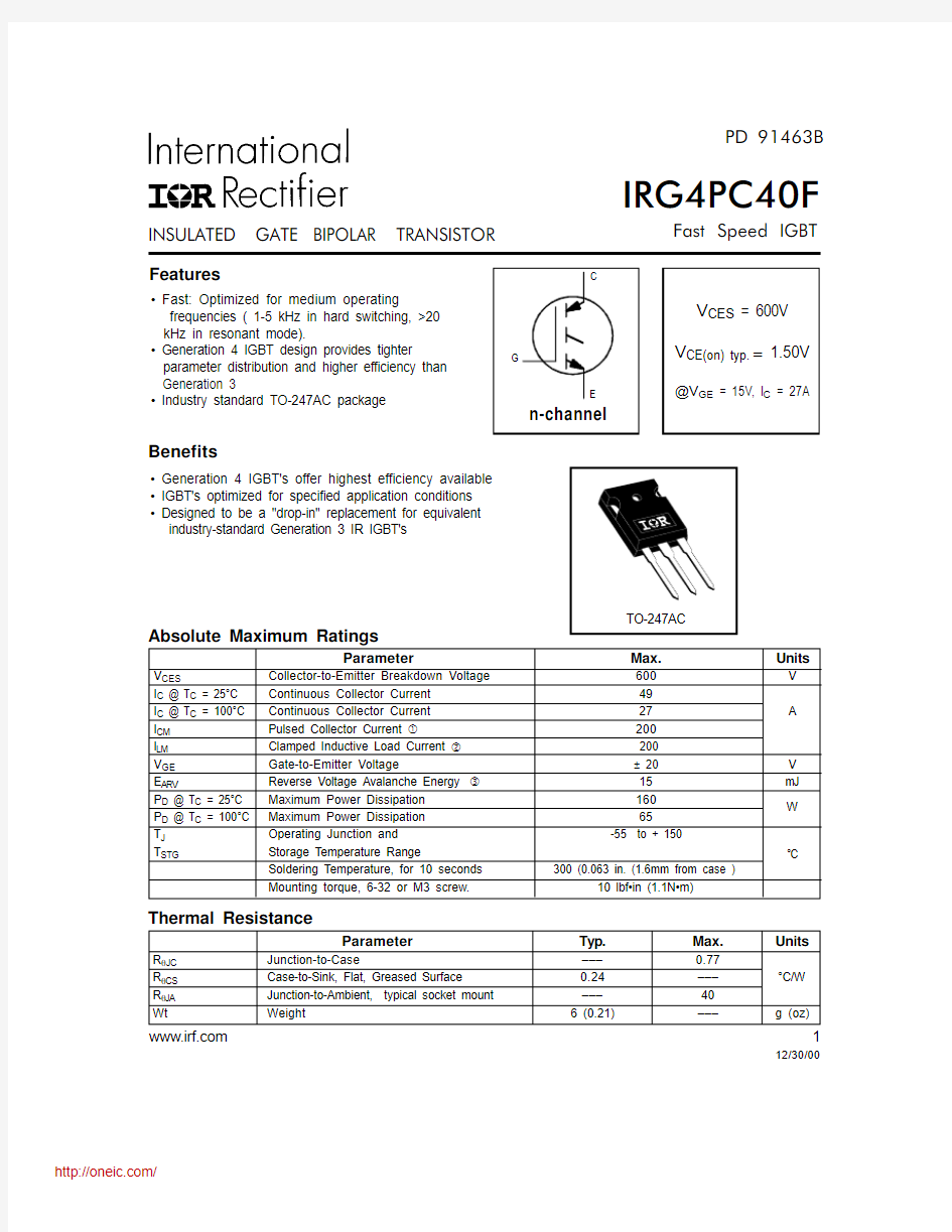
IRG4PC40F
Fast Speed IGBT
INSULATED GATE BIPOLAR TRANSISTOR
PD 91463B
Features
? Fast: Optimized for medium operating
frequencies ( 1-5 kHz in hard switching, >20 kHz in resonant mode).
? Generation 4 IGBT design provides tighter
parameter distribution and higher efficiency than Generation 3
? Industry standard TO-247AC package
?? IGBT's optimized for specified application conditions ? Designed to be a "drop-in" replacement for equivalent industry-standard Generation 3 IR IGBT's
Benefits
12/30/00
Parameter
Typ.
Max.
Units
R θJC Junction-to-Case
–––0.77R θCS Case-to-Sink, Flat, Greased Surface
0.24–––°C/W R θJA Junction-to-Ambient, typical socket mount –––40Wt
Weight
6 (0.21)
–––
g (oz)
Thermal Resistance
Absolute Maximum Ratings
W
https://www.doczj.com/doc/af12173401.html, 1
IRG4PC40F
https://www.doczj.com/doc/af12173401.html,
Parameter
Min.Typ.Max.Units Conditions Q g Total Gate Charge (turn-on)—100150I C = 27A Q ge Gate - Emitter Charge (turn-on)—1523nC V CC = 400V See Fig. 8Q gc Gate - Collector Charge (turn-on)—3553V GE = 15V t d(on)Turn-On Delay Time —26—t r Rise Time
—18—T J = 25°C
t d(off)Turn-Off Delay Time —240360I C = 27A, V CC = 480V t f Fall Time
—170250V GE = 15V, R G = 10?E on Turn-On Switching Loss —0.37—Energy losses include "tail"E off Turn-Off Switching Loss — 1.81—mJ See Fig. 10, 11, 13, 14E ts Total Switching Loss — 2.18 2.8t d(on)Turn-On Delay Time —25—T J = 150°C,t r Rise Time
—21—I C = 27A, V CC = 480V
t d(off)Turn-Off Delay Time —380—V GE = 15V, R G = 10?t f Fall Time
—310—Energy losses include "tail"E ts Total Switching Loss
— 3.9—mJ See Fig. 13, 14L E Internal Emitter Inductance —13—nH Measured 5mm from package C ies Input Capacitance —2200—V GE = 0V C oes Output Capacitance
—140—pF V CC = 30V See Fig. 7C res Reverse Transfer Capacitance
—
29
—? = 1.0MHz
Parameter Min.Typ.
Max.Units Conditions
V (BR)CES Collector-to-Emitter Breakdown Voltage 600—
—V V GE = 0V, I C = 250μA V (BR)ECS
Emitter-to-Collector Breakdown Voltage T 18——V V GE = 0V, I C = 1.0A ?V (BR)CES /?T J Temperature Coeff. of Breakdown Voltage —0.70
—V/°C V GE = 0V, I C = 1.0mA — 1.50
1.7 I C = 27A V GE = 15V V CE(ON)Collector-to-Emitter Saturation Voltage — 1.85
— I C = 49A See Fig.2, 5
— 1.56
— I C = 27A , T J = 150°C V GE(th)Gate Threshold Voltage 3.0— 6.0V CE = V GE , I C = 250μA ?V GE(th)/?T J Temperature Coeff. of Threshold Voltage —-12—mV/°C V CE = V GE , I C = 250μA g fe Forward Transconductance U 9.212
—S V CE = 100V, I C = 27A ——
250V GE = 0V, V CE = 600V
—— 2.0V GE = 0V, V CE = 10V, T J = 25°C ——
1000V GE = 0V, V CE = 600V, T J = 150°C I GES Gate-to-Emitter Leakage Current ——
±100nA V GE = ±20V
Electrical Characteristics @ T J = 25°C (unless otherwise specified)
I CES Zero Gate Voltage Collector Current
V
μA
Switching Characteristics @ T J = 25°C (unless otherwise specified)
ns
ns
T Pulse width ≤ 80μs; duty factor ≤ 0.1%.U Pulse width 5.0μs, single shot.
Notes:
Q Repetitive rating; V GE = 20V, pulse width limited by
max. junction temperature. ( See fig. 13b )
R V CC = 80%(V CES ), V GE = 20V, L = 10μH, R G = 10?,
(See fig. 13a)
S Repetitive rating; pulse width limited by maximum
junction temperature.
IRG4PC40F
https://www.doczj.com/doc/af12173401.html,
3
Fig. 1 - Typical Load Current vs. Frequency
(For square wave, I=I RMS of fundamental; for triangular wave, I=I PK )
Fig. 2 - Typical Output Characteristics Fig. 3 - Typical Transfer Characteristics
110
100
1000
5
6
7
8
9
10
11
12
C
I , C o l l e c t o r -t o -E m i t t e r C u r r e n t (A )GE
V , Gate-to-Emitter Voltage (V)020
40
60
80
0.1
1
10
100
f, Frequency (kHz)
L o a d C u r r e n t (A )
110
100
1000
1
10
CE
V , Collector-to-Em itter V oltage (V )I C , C o l l e c t o r -t o -E m i t t e r C u r r e n t (A )
IRG4PC40F
4
https://www.doczj.com/doc/af12173401.html,
Fig. 6 - Maximum Effective Transient Thermal Impedance, Junction-to-Case
Fig. 5 - Typical Collector-to-Emitter Voltage
vs. Junction Temperature
Fig. 4 - Maximum Collector Current vs. Case
Temperature
010
20
30
40
50
25
50
75
100
125
150
M a x i m u m D C C o l l e c t o r C u r r e n t (A )
T , C ase Tem perature (°C)C
1.01.5
2.0
2.5
-60
-40
-20
20
40
60
80
100120140160
C E V , C o l l e c t o r -t o -E m i t t e r V o l t a g e (V )
T , Junction Temperature (°C)J
0.01
0.1
1
0.00001
0.00010.0010.010.1110
t , Rectangular Pulse Duration (sec)1
t h J C
T h e r m a l R e s p o n s e (Z )
IRG4PC40F
https://www.doczj.com/doc/af12173401.html,
5
Fig. 10 - Typical Switching Losses vs.
Junction Temperature
Fig. 9 - Typical Switching Losses vs. Gate
Resistance Fig. 8 - Typical Gate Charge vs.
Gate-to-Emitter Voltage
Fig. 7 - Typical Capacitance vs.
Collector-to-Emitter Voltage 04
8
12
16
20
20
40
60
80
100
120
G E V , G a t e -t o -E m i t t e r V o l t a g e (V )
g
Q , Total Gate Charge (nC)
0.11
10
-60
-40
-20
20
40
60
80
100
120
140
160
T o t a l S w i t c h i n g L o s s e s (m J )
T , Junction Temperature (°C)J
2.10
2.20
2.30
2.40
2.50
2.60
10
20
30
40
50
60
R , Gate Resistance (?)G
T o t a l S w i t c h i g L o s s e s (m J )
01000
2000
3000
4000
1
10
100
CE V , Collector-to-Emitter Voltage (V)C , C a p a c i t a n c e ( p F )
IRG4PC40F
https://www.doczj.com/doc/af12173401.html,
Fig. 12 - Turn-Off SOA
Fig. 11 - Typical Switching Losses vs.
Collector-to-Emitter Current
02
4
6
8
10
10
20
30
40
50
60
C T o t a l S w i t c h i n g L o s s e s (m J )
I , Collector-to-Emitter Current (A)110
100
1000
1
10
100
1000
C
C E
V , Collector-to-Em itter Voltage (V)I , C o l l e c t o r -t o -E m i t t e r C u r r e n t (A )
IRG4PC40F
https://www.doczj.com/doc/af12173401.html, 7
480V
X C @
* Note: Due to the 50V pow er supply, pulse width and inductor w ill increase to obtain rated Id.
Fig. 13a - Clamped Inductive
Load Test Circuit
Fig. 13b - Pulsed Collector
Current Test Circuit
=
ts o n off
E = (E +E )Fig. 14b - Switching Loss
Waveforms
Fig. 14a - Switching Loss
Test Circuit
* Driver same type as D.U.T., VC = 480V
IRG4PC40F
https://www.doczj.com/doc/af12173401.html,
Case Outline and Dimensions TO-247AC
D im e n sion s in M illim e te rs a n d (In ch es )
CONFORMS TO JEDEC OUTLINE TO-247AC (TO-3P)
- D -
5.30 (.209)4.70 (.185)3.65 (.143)3.55 (.140)
2.50 (.089)1.50 (.059)
4
3X
0.80 (.031)0.40 (.016)2.60 (.102)2.20 (.087)
3.40 (.133)3.00 (.118)
3X
0.25 (.010)M
C A S
4.30 (.170)3.70 (.145)
- C -
2X
5.50 (.217)4.50 (.177)
5.50 (.217)
0.25 (.010)1.40 (.056)1.00 (.039)D M M
B - A -15.90 (.626)15.30 (.602)
- B -
1
2
3
20.30 (.800)19.70 (.775)
14.80 (.583)14.20 (.559)
2.40 (.094)2.00 (.079)
2X 2X
5.45 (.215)
*
N O TE S :
1 D IM E N S IO N S & T O LE R A N C IN G P E R A N S I Y 14.5M , 1982.
2 C O N TR O LLIN G D IM E N S IO N : IN C H.
3 D IM E N S IO N S A R E S H O W N M ILLIM E TE R S (IN C H E S ).
4 C O N FO R M S TO
JE D E C O U TLIN E T O -247AC.
LE A D A S S IG N M E N T S 1 - G A T E
2 - C O LLE C TO R
3 - EM IT TE R
4 - C O LLE C TO R
*
LO N G E R LE A D ED (20m m )
V E R S IO N A V A ILA B LE (TO -247A D )T O O R D E R A D D "-E " S U FF IX T O P A R T N U M B ER
IR WORLD HEADQUARTERS: 233 Kansas St., El Segundo, California 90245, USA Tel: (310) 252-7105
TAC Fax: (310) 252-7903
Visit us at https://www.doczj.com/doc/af12173401.html, for sales contact information .
Data and specifications subject to change without notice. 12/00
Note: For the most current drawings please refer to the IR website at:
https://www.doczj.com/doc/af12173401.html,/package/
分销商库存信息: IR
IRG4PC40F