GS841E18AT/B-180/166/150/130/100
256K x 18 Sync Cache Tag 180 MHz–100 MHz
3.3 V V DD
3.3 V and 2.5 V I/O
TQFP, BGA
Commercial Temp Industrial Temp Features
? 3.3 V +10%/–5% core power supply, 2.5 V or 3.3 V I/O supply
? Dual Cycle Deselect (DCD)
? Intergrated data comparator for Tag RAM application ? FT mode pin for flow through or pipeline operation
? LBO pin for Linear or Interleave (Pentium TM and X86) Burst mode
? Synchronous address, data I/O, and control inputs ? Synchronous Data Enable (DE)? Asynchronous Output Enable (OE)
? Asynchronous Match Output Enable (MOE)
? Byte Write (BWE) and Global Write (GW) operation ? Three chip enable signals for easy depth expansion ? Internal self-timed write cycle
? JTAG Test mode conforms to IEEE standard 1149.1? JEDEC-standard 100-lead TQFP package and 119-BGA ? Pb-Free 100-lead TQFP package available
Functional Description
The GS841E18A is a 256K x 18 high performance synchronous DCD SRAM with integrated Tag RAM comparator. A 2-bit burst counter is included to provide burst interface with Pentium TM and other high performance CPUs. It is designed to be used as a Cache Tag SRAM, as well as data SRAM. Addresses, data IOs, match output, chip enables (CE1, CE2, CE3), address control inputs (ADSP, ADSC, ADV), and write control inputs (BW1, BW2, BWE, GW, DE) are synchronous and are controlled by a positive-edge-triggered clock (CLK).
Output Enable (OE), Match Output Enable, and power down control (ZZ) are asynchronous. Burst can be initiated with either ADSP or ADSC inputs. Subsequent burst addresses are generated internally and are controlled by ADV. The burst sequence is either interleave order (Pentium TM or x86) or linear order, and is controlled by LBO.
Output registers and the Match output register are provided and
controlled by the FT mode pin (Pin 14). Through use of the FT mode pin, I/O registers can be programmed to perform pipeline or flow through operation. Flow Through mode reduces latency.
Byte write operation is performed by using Byte Write Enable (BWE) input combined with two individual byte write signals BW1-2. In addition, Global Write (GW) is available for writing all bytes at one time.
Compare cycles begin as a read cycle with output disabled so that compare data can be loaded into the data input register. The
comparator compares the read data with the registered input data and a match signal is generated. The match output can be either in Pipeline or Flow Through modes controlled by the FT signal.
Low power (Standby mode) is attained through the assertion of the ZZ signal, or by stopping the clock (CLK). Memory data is retained during Standby mode.
JTAG boundary scan interface is provided using IEEE standard 1149.1 protocol. Four pins—Test Data In (TDI), Test Data Out
(TDO), Test Clock (TCK) and Test Mode Select (TMS)—are used to perform JTAG function.
The GS841E18A operates on a 3.3 V power supply and all inputs/outputs are 3.3 V- or 2.5 V-LVTTL-compatible. Separate output (V DDQ ) pins are used to allow both 3.3 V or 2.5 V IO interface.
Dual Cycle Deselect (DCD)
The GS841E18A is a DCD pipelines synchronous SRAM. DCD SRAMs pipeline disable commands to the same degree as read commands. DCD SRAMs hold the deselect command for one full cycle and then begin turning off their outputs just after the second rising edge of the clock.
Parameter Synopsis
–180
-166-150-133-100Pipeline 3-1-1-1t cycle t KQ I DD 5.5 ns 3.2 ns 335 mA 6.0 ns 3.5 ns 310 mA 6.6 ns 3.8 ns 275 mA 7.5 ns 4.0 ns 250 mA 10 ns 4.5 ns 190 mA Flow Through 2-1-1-1
t KQ t cycle I DD
8 ns 9.1 ns 210 mA
8.5 ns 10 ns 190 mA
10 ns 10 ns 190 mA
11 ns 15 ns 140 mA
12 ns 15 ns 140 mA
GS841E18AT/B-180/166/150/130/100
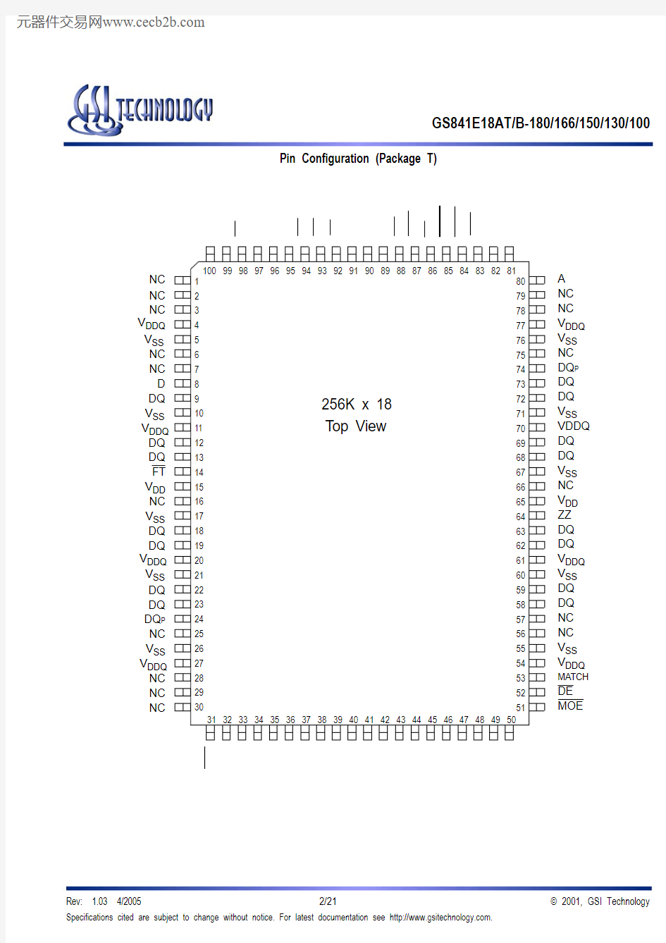
Pin Configuration (Package T)
807978777675747372
7170
69686766656463626160595857565554535251123456789101112131415161718192021222324252627282930V DDQ V SS D DQ V SS V DDQ DQ DQ V DD NC V SS DQ DQ V DDQ V SS DQ DQ DQ P V SS V DDQ V DDQ V SS DQ DQ V SS VDDQ DQ DQ V SS NC V DD ZZ DQ DQ V DDQ V SS DQ DQ V SS V DDQ
L B O A A A A A 1
A 0
T M S T D I V S S
V D D
T D O T C K A A A A A A
A A C E 1
C E 2 N C N C B W 2
B W 1
C E 3
C L K G W B W E V
D D
V S S
O E A D S C A D S P A D V A A
A 256K x 18Top View DQ P A NC NC NC NC NC DE MATCH
MOE
NC NC NC NC NC NC NC
NC NC 100999897969594939291908988878685848382813132333435363738394041424344454647484950
FT
GS841E18AT/B-180/166/150/130/100 GS841E18A PadOut—119-Bump BGA—Top View (Package B)
1234567
A V DDQ A A ADSP A A V DDQ
B N
C E2A ADSC A E3NC
C NC A A V D
D A A NC
D DQ B NC V SS NC V SS DQ P NC
E NC DQ B V SS E1V SS NC DQ A
F V DDQ NC V SS
G V SS DQ A V DDQ
G NC D Q B B B ADV NC NC DQ A
H DQ B N C V SS GW V SS DQ A NC
J V DDQ V DD NC V DD NC V DD V DDQ
K NC DQ B V SS CK V SS NC DQ A
L DQ B NC NC NC B A DQ A NC
M V DDQ DQ B V SS BW V SS MATCH V DDQ
N DQ B NC V SS A1V SS DQ A DE
P NC DQ P V SS A0V SS MOE DQ A
R NC A LBO V DD FT A NC
T NC A A NC A A ZZ
U V DDQ TMS TDI TCK TDO NC V DDQ
GS841E18AT/B-180/166/150/130/100
TQFP Pin Description
Symbol Description
An Address Input Signals—Inputs are registered and must meet setup and hold times, as specified on
page 11.
CLK Clock Input Signal
BWE Byte Write Enable Signal—The byte write enable signal needs to be combined with one of the four
byte write signals for a write operation to occur.
BW1Byte Write signal for data outputs 1 thru 8
BW2Byte Write signal for data outputs 9 thru 16
GW Global Write Enable
CE1,CE2, CE3Chip Enables
OE Output Enable
ADV Burst address advance
ADSP, ADSC Address status signals
DQ Data Input and Output pins
DQP Parity Input and Output pins
MATCH Match Output
MOE Match Output Enable
DE Data Enable—Data input registers are updated only when DE is active.
ZZ Power down control—Application of ZZ will result in a low standby power consumption.
FT Flow Through or Pipeline mode
LBO Linear Order Burst mode
TMS Test Mode Select
TDI Test Data In
TDO Test Data Out
TCK Test Clock
V DD 3.3 V power supply
V SS Ground
V DDQ 2.5 V/3.3 V output power supply
NC No Connect
GS841E18AT/B-180/166/150/130/100
PBGA Pin Description
Symbol Description
An Address Input Signals—Inputs are registered and must meet setup and hold times, as specified on
page 11.
CLK Clock Input Signal
BWE Byte Write Enable Signal—The byte write enable signal needs to be combined with one of the four
byte write signals for a write operation to occur.
BW1Byte Write signal for data outputs 1 thru 8
BW2Byte Write signal for data outputs 9 thru 16
GW Global Write Enable
CE1,CE2, CE3Chip Enables
OE Output Enable
ADV Burst address advance
ADSP, ADSC Address status signals
DQ Data Input and Output pins
DQP Parity Input and Output pins
MATCH Match Output
MOE Match Output Enable
DE Data Enable—Data input registers are updated only when DE is active.
ZZ Power down control—Application of ZZ will result in a low standby power consumption.
FT Flow Through or Pipeline mode
LBO Linear Order Burst mode
TMS Test Mode Select
TDI Test Data In
TDO Test Data Out
TCK Test Clock
V DD 3.3 V power supply
V SS Ground
V DDQ 2.5 V/3.3 V output power supply
NC No Connect
GS841E18AT/B-180/166/150/130/100
Functional Block Diagram
A1
A0
A0A1
D0
D1
Q1
Q0B INARY C OUNTER
Load
D Q
R EGISTE R
D Q
Register D Q
Register D Q
Register D Q
Register D Q
Register D
Q
Register
D
Q
Register
A0-17
LBO ADV CLK ADSC ADSP
GW BWE BW1
BW2
CE1
CE2CE3FT
DQ1-16OE ZZ
Powerdown Control
256K X 18
Memory Array
18
1818
18
2
18
A
Q
D
DQP1-2
DE
D
Q
Register
Match
TAP Controller
Instruction Reg.
ID Reg.Bypass Reg Boundary Scan Registers 54
TCK
TMS TDI
A, DQ, Control
TDO
MOE always (?)
GS841E18AT/B-180/166/150/130/100
Mode Pin Function
LBO
Function
L Linear Burst H or NC
Interleaved Burst
FT
Function
L Flow Through H or NC
Pipeline
Power Down Control
Note:
There are pull up devices on LBO and FT pins and pull down device on ZZ pin, so those input pins can be unconnected and the chip will operate in the default states as specified in the above tables.
ZZ
Function
L or NC Active H
Standby, IDD = ISB
Linear Burst Sequence
A[1:0]A[1:0]A[1:0]A[1:0]
1st address 000110112nd address 011011003rd address 101100014th address
11
00
01
10
Interleaved Burst Sequence
A[1:0]A[1:0]A[1:0]A[1:0]
1st address 000110112nd address 010011103rd address 101100014th address
11
10
01
00
Note: H = logic high, L = logic low, NC = no connect
Byte Write Function
Function
GW
BWE
BW1
BW2
Read H H X X Read H L H H Write all bytes L X X X Write all bytes H L L L Write byte 1H L L H Write byte 2
H
L
H
L
GS841E18AT/B-180/166/150/130/100
Notes:
1.X means “don’t care,” H means “logic high,” L means “logic low.”
2.Write is the logic function of GW, BWE, BW1, BW2. See Byte Write Function table for detail.
3.All inputs, except OE, must meet setup and hold on rising edge of CLK.
4.Suspending busrt generates a wait cycle.
5.ADSP LOW along with SRAM being selected always initiates a Read cycle at the L-H edge of the clock (CLK).
6.
A Write cycle can only be performed by setting Write low for the clock L-H edge of the subsequent wait cycle. Refer to page 12 for the Write timing diagram.
Synchronous Truth Table
Operation
Address Used
CE1CE2CE3ADSP ADSC ADV Write OE CLK DQ Deselect Cycle, Power Down none H X X X L X X X L-H High-Z Deselect Cycle, Power Down none L L X L X X X X L-H High-Z Deselect Cycle, Power Down none L X H L X X X X L-H High-Z Deselect Cycle, Power Down none L L X H L X X X L-H High-Z Deselect Cycle, Power Down none L X H H L X X X L-H High-Z Read Cycle, Begin Burst external L H L L X X X L L-H Q Read Cycle, Begin Burst external L H L L X X X H L-H High-Z Read Cycle, Begin Burst external L H L H L X H L L-H Q Read Cycle, Begin Burst external L H L H L X H H L-H High-Z Write Cycle, Begin Burst external L H L H L X L X L-H D Read Cycle, Continue Burst next X X X H H L H L L-H Q Read Cycle, Continue Burst next X X X H H L H H L-H High-Z Read Cycle, Continue Burst next H X X X H L H L L-H Q Read Cycle, Continue Burst next H X X X H L H H L-H High-Z Write Cycle, Continue Burst next X X X H H L L X L-H D Write Cycle, Continue Burst next H X X X H L L X L-H D Read Cycle, Suspend Burst current X X X H H H H L L-H Q Read Cycle, Suspend Burst current X X X H H H H H L-H High-Z Read Cycle, Suspend Burst current H X X X H H H L L-H Q Read Cycle, Suspend Burst current H X X X H H H H L-H High-Z Write Cycle, Suspend Burst current X X X H H H L X L-H D Write Cycle, Suspend Burst
current
H
X
X
X
H
H
L
X
L-H
D
GS841E18AT/B-180/166/150/130/100
Notes:
1.X means “don’t care,” H means “logic high,” L means “logic low.”
2.Write is the logic function of GW, BWE, BW1, BW2. See Byte Write Function table for detail.
3.CE is defined as CE1=L, CE2=H and CE3=L
4.All signals are synchronous and are sampled by CLK except OE and MOE. OE and MOE are asynchronous and drive the bus immediately.
)
Note:
Permanent damage to the device may occur if the Absolute Maximun Ratings are exceeded. Functional operation should be restricted to the recommended operation conditions. Exposure to higher than recommended voltages, for an extended period of time, could effect the performance and reliability of this component.
Truth Table For Read/Write/Compare/Fill Write Operation
CE
Write
DE
MOE
OE
Match
DQ
Read L H X X L —Q Write L L L X H —D Compare L H L L H Data Out D Fill Write L L H X X —X Match Deselect H X X L X High High Z Deselect
H
X
X
H
X
High Z
High Z
Absolute Maximum Ratings (Voltage reference to V SS = 0 V)
Symbol
Description
Commerical
Unit
V DD Supply Voltage –0.5 to 4.6V V DDQ Output Supply Voltage –0.5 to V DD V V CLK CLK Input Voltage –0.5 to 6V V in Input Voltage –0.5 to V DD + 0.5 (≤ 4.6 V max. )V V out Output Voltage –0.5 to V DD + 0.5 (≤ 4.6 V max. )
V I out Output Current per I/O +/–20mA P D Power Dissipation 1.5W
T OPR Operating Temperature 0 to 70o C T STG
Storage Temperature
–55 to 125
o
C
GS841E18AT/B-180/166/150/130/100
Notes:
1.Junction temperature is a function of SRAM power dissapation, package thermal resistance, mounting board temperature, ambient. Temperature air flow, board density, and PCB thermal resistance.
2.SCMI G-38-87.
3.
Average thermal resistance between die and top surface, MIL SPEC-883, Method 1012.1.
Package Thermal Characteristics
Rating
Layer Board
Symbol
TQFP max
PBGA max
Unit
Notes
Junction to Ambient (at 200 lfm)single R ΘJA 3228°C/W 1,2Junction to Ambient (at 200 lfm)
four R ΘJA 2018°C/W 1,2Junction to Case (TOP)
—
R ΘJC
7
4
°C/W
3
Notes: 1.Include scope and jig capacitance.
2.Test conditions as specified with output loading as shown in Fig. 1 unless otherwise noted.
3.Output load 2 for t LZ , t HZ , t OLZ and t OHZ .
4.
Device is deselected as defined by the Truth Table.
AC Test Conditions
(VDD = 3.135 V–3.6 V, Ta = 0–70°C)
Parameter
Conditions
Input high level V IH = 2.3 V Input low level V IL = 0.2 V Input slew rate TR = 1 V/ns Input reference level 1.25 V Output reference level
1.25 V Output load
Fig. 1& 2
DQ
VT = 1.25 V
50W 30pF 1
DQ
2.5 V F IG . 1
Output load 1
Output load 2F IG . 2225W 225W
5pF 1
GS841E18AT/B-180/166/150/130/100
DC Characteristics and Supply Currents(Voltage reference to V SS = 0 V)
(VDD = 3.135 V–3.6 V, Ta = 0–70°C for Commercial Temperature Offering)
Parameter Symbol Test Conditions Min Max
Input Leakage Current
(except ZZ, FT, LBO pins)
I IL V IN = 0 to V DD–1 uA 1 uA
ZZ Input Current Iin ZZ V DD ≥V IN ≥V IH
0 V≤ V IN ≤ V IH
–1 uA
–1 uA
1 uA
300 uA
Mode Input Current (FT & LBO pins)Iin M
V DD ≥V IN ≥V IL
0 V≤ V IN ≤ V IL
–30 0uA
–1 uA
1 uA
1 uA
Output Leakage Current I ol Output Disable,
V OUT = 0 to V DD–1 uA 1 uA
Output High Voltage V OH I OH = –4 mA, V DDQ = 2.375 V 1.7 V
Output High Voltage V OH I OH = –4 mA, V DDQ = 3.135 V 2.4 V
Output Low Voltage V OL I OL = +4 mA0.4 V
GS841E18AT/B-180/166/150/130/100
Operating Currents
Parameter Test Conditions Symbol
-180-166-150-133-100
Unit 0
to
70°C
–40
to
85°C
to
70°C
–40
to
+85°C
to
70°C
–40
to
+85°C
to
70°C
–40
to
+85°C
to
70°C
–40
to
+85°C
O perating Current Device Selected;
All other inputs
≥ V IH O r ≤ V IL
Output open
I DD
Pipeline
335345310320275285250260190200mA
I DD
Flow
Through
210220190200190200140150140150mA
Standby Current ZZ≥ V DD – 0.2 V
I SB
Pipeline
20303040304030403040mA
I SB
Flow
Through
20303040304030403040mA
Deselect Supply Current Device Deselected;
All other inputs
≥ V IH OR≤ V IL
I DD
Pipeline
55651101201051151001108090mA
I DD
Flow
Through
40508090809065756575mA
GS841E18AT/B-180/166/150/130/100
Notes:
1.These parameters are sampled and are not 100% tested
2.ZZ is an asynchronous signal. However, in order to be recognized on any given clock cycle, ZZ must meet the specified setup and hold
times as specified above.
AC Electrical Characteristics
Parameter
Symbol
-180-166-150-133-100Unit
Min
Max
Min
Max
Min
Max
Min
Max
Min
Max
Pipeline
Clock Cycle Time tKC 5.5— 6.0— 6.7—7.5—10—ns Clock to Output Valid tKQ — 3.2— 3.5— 3.8—4— 4.5ns Clock to Output Invalid
tKQX 1.5— 1.5— 1.5— 1.5— 1.5—ns Clock to Output in Low-Z tLZ 1 1.5— 1.5— 1.5— 1.5— 1.5—ns Clock to Match Valid tKM — 3.2— 3.5— 3.8—4— 4.5ns Clock to Match Invalid tKMX 1.5— 1.5— 1.5— 1.5— 1.5—ns Clock to Match in Low-Z tMLZ 1 1.5— 1.5— 1.5— 1.5— 1.5—ns Flow Through
Clock Cycle Time tKC 9.1—10.0—10.0—15.0—15.0—ns Clock to Output Valid tKQ —8.0—8.5—10.0—11.0—12.0ns Clock to Output Invalid
tKQX 3.0— 3.0— 3.0— 3.0— 3.0—ns Clock to Output in Low-Z tLZ 1 3.0— 3.0— 3.0— 3.0— 3.0—ns Clock to Match Valid tKM —8.5—8.5—10.0—11.0—12.0ns Clock to Match Invalid tKMX 3.0— 3.0— 3.0— 3.0— 3.0—ns Clock to Match in Low-Z tMLZ 1 3.0— 3.0— 3.0— 3.0— 3.0—ns Clock HIGH Time tKH 1.3— 1.3— 1.5— 1.7—2—ns Clock LOW Time tKL 1.5— 1.5— 1.7
—
1.9—
2.2—ns Clock to Output in High-Z tHZ 1 1.5
3.2 1.5 3.5 1.5 3.8 1.54 1.55ns OE to Output Valid tOE — 3.2— 3.5— 3.8—4—5ns OE to output in Low-Z tOLZ 10—0—0—0—0—ns OE to output in High-Z tOHZ 1— 3.2— 3.5— 3.8—4—5ns MOE to Match Valid tMOE — 3.2— 3.5— 3.8—4—5ns MOE to Match in Low-Z tMOLZ 10—0—0—0—0—ns MOE to Match in High-Z
tMOHZ 1— 3.2— 3.5— 3.8—4—5ns Setup time tS 1.5— 1.5— 1.5— 2.0— 2.0—ns Hold time tH 0.5—0.5—0.5—0.5—0.5—ns ZZ setup time tZZS 25—5—5—5—5—ns ZZ hold time tZZH 21—1—1—1—1—ns ZZ recovery
tZZR
20
—
20
—
20
—
20
—
20
—
ns
GS841E18AT/B-180/166/150/130/100
Pipeline Mode Timing
Begin Read A Cont Deselect Deselect Write B
Read C Read C+1Read C+2Read C+3Cont Deselect Deselect
tHZ
tKQX
tKQ
tLZ
tH
tS
tOHZ
tOE
tH
tS
tH
tS
tH
tS
tH tS
tH
tS
tS
tH
tS
tH
tS
tH
tS
tKC
tKL tKH
Q(A)
D(B)
Q(C)
Q(C+1)
Q(C+2)
Q(C+3)
A
B
C
Hi-Z
Deselected with E1
E2 and E3 only sampled with ADSC
ADSC initiated read
CK ADSP
ADSC
ADV
Ao–An
GW
BW
Ba–Bd
E1
E2
E3G
DQa–DQd
GS841E18AT/B-180/166/150/130/100
Flow Through Mode Timing
Begin Read A Cont
Deselect Write B Read C Read C+1Read C+2Read C+3Read C Deselect
tHZ
tKQX tLZ
tH tS
tOHZ
tOE tKQ
tH
tS tH
tS tH
tS
tH tS
tH
tS tH
tS
tH
tS tH
tS tH tS
tH tS tH
tS tKC
tKL tKH
A
B
C
Q(A)
D(B)
Q(C)
Q(C+1)
Q(C+2)
Q(C+3)
Q(C)
E2 and E3 only sampled with ADSP and ADSC
E1 masks ADSP
ADSC initiated read
Deselected with E1
E1 masks ADSP
Fixed High
CK ADSP
ADSC
ADV
Ao–An
GW
BW
Ba–Bd
E1
E2
E3G
DQa–DQd
GS841E18AT/B-180/166/150/130/100
Pipeline Compare Fill Write Cycle
Hit Miss Fill Write
A B
B
A A tKM
tKM
tKMX
tKM tMOE tMLZ
tH tS
tH tS
tH tS
tH tS
tH tS
K
Address
DQ
CE
W G
DE MOE
Match
GS841E18AT/B-180/166/150/130/100
Flow Through Compare Fill Write Cycle
Hit Miss Fill Write
A B
B
A A tKM
tKM tKMX
tKM tMOE tMLZ
tH tS
tH tS
tH tS
tH tS
tH tS
K
Address
DQ
CE
W G
DE MOE
Match
GS841E18AT/B-180/166/150/130/100
TQFP Package Drawing (Package T)
D1
D E1E
Pin 1
b
e c
L
L1
A2
A1
Y
θ
Notes:
1.All dimensions are in millimeters (mm).
2.Package width and length do not include mold protrusion.
Symbol
Description
Min.Nom.Max
A1Standoff 0.050.100.15A2Body Thickness 1.35 1.40 1.45b Lead Width 0.200.300.40c Lead Thickness 0.09—0.20D Terminal Dimension 21.922.022.1D1Package Body 19.920.020.1E Terminal Dimension 15.916.016.1E1Package Body 13.914.014.1e Lead Pitch —0.65—L Foot Length 0.450.600.75L1Lead Length —
1.00
—Y Coplanarity 0.10
θ
Lead Angle
0°
—
7°
GS841E18AT/B-180/166/150/130/100
Package Dimensions—119-Bump FPBGA (Package B, Variation 2)
A B C D E F G H J K L M N P R T U
1 2 3 4 5 6 7
7 6 5 4 3 2 1
A1 TOP VIEW
A1 BOTTOM VIEW 1.277.62
1.27
20.32
14±0.10
22±0.10
B
A 0.20(4x)
?0.10?0.30C
C A B S S ?0.60~0.90 (119x)
C
SEATING PLANE
0.15C
0.50~0.701.86.±0.13
0.70±0.050.15C
A B C D E F G H J K L M N P R T U
0.56±0.05
S S
GS841E18AT/B-180/166/150/130/100 Ordering Information
Org Part Number1Type Package Speed 2
(MHz/ns)T A
3
Status
256K x 18GS841E18AT-180DCD Pipeline/Flow Through TQFP180/8C
256K x 18GS841E18AT-166DCD Pipeline/Flow Through TQFP166/8.5C
256K x 18GS841E18AT-150DCD Pipeline/Flow Through TQFP150/10C
256K x 18GS841E18AT-133DCD Pipeline/Flow Through TQFP133/11C
256K x 18GS841E18AT-100DCD Pipeline/Flow Through TQFP100/12C
256K x 18GS841E18AT-180I DCD Pipeline/Flow Through TQFP180/8I
256K x 18GS841E18AT-166I DCD Pipeline/Flow Through TQFP166/8.5I
256K x 18GS841E18AT-150I DCD Pipeline/Flow Through TQFP150/10I
256K x 18GS841E18AT-133I DCD Pipeline/Flow Through TQFP133/11I
256K x 18GS841E18AT-100I DCD Pipeline/Flow Through TQFP100/12I
256K x 18GS841E18AGT-180DCD Pipeline/Flow Through Pb-Free TQFP180/8C
256K x 18GS841E18AGT-166DCD Pipeline/Flow Through Pb-Free TQFP166/8.5C
256K x 18GS841E18AGT-150DCD Pipeline/Flow Through Pb-Free TQFP150/10C
256K x 18GS841E18AGT-133DCD Pipeline/Flow Through Pb-Free TQFP133/11C
256K x 18GS841E18AGT-100DCD Pipeline/Flow Through Pb-Free TQFP100/12C
256K x 18GS841E18AGT-180I DCD Pipeline/Flow Through Pb-Free TQFP180/8I
256K x 18GS841E18AGT-166I DCD Pipeline/Flow Through Pb-Free TQFP166/8.5I
256K x 18GS841E18AGT-150I DCD Pipeline/Flow Through Pb-Free TQFP150/10I
256K x 18GS841E18AGT-133I DCD Pipeline/Flow Through Pb-Free TQFP133/11I
256K x 18GS841E18AGT-100I DCD Pipeline/Flow Through Pb-Free TQFP100/12I
256K x 18GS841E18AB-180DCD Pipeline/Flow Through119 BGA (var. 2)180/8C
256K x 18GS841E18AB-166DCD Pipeline/Flow Through119 BGA (var. 2)166/8.5C
256K x 18GS841E18AB-150DCD Pipeline/Flow Through119 BGA (var. 2)150/10C
256K x 18GS841E18AB-133DCD Pipeline/Flow Through119 BGA (var. 2)133/11C
256K x 18GS841E18AB-100DCD Pipeline/Flow Through119 BGA (var. 2)100/12C
256K x 18GS841E18AB-180I DCD Pipeline/Flow Through119 BGA (var. 2)180/8I
256K x 18GS841E18AB-166I DCD Pipeline/Flow Through119 BGA (var. 2)166/8.5I
256K x 18GS841E18AB-150I DCD Pipeline/Flow Through119 BGA (var. 2)150/10I
256K x 18GS841E18AI-133I DCD Pipeline/Flow Through119 BGA (var. 2)133/11I
256K x 18GS841E18AB-100I DCD Pipeline/Flow Through119 BGA (var. 2)100/12I
Notes:
1.Customers requiring delivery in Tape and Reel should add the character “T” to the end of the part number. Example: GS841E18AT-166T.
2.The speed column indicates the cycle frequency (Mhz) of the device in Pipelined mode and the latency (ns) in Flow Through mode. Each
device is Pipeline / Flow through mode selectable by the user.
3.T A = C = Commercial Temperature Range. T A = I = Industrial Temperature Range.
4. GSI offers other versions this type of device in many different configurations and with a variety of different features, only some of which
are covered in this data sheet. See the GSI Technology web site for a complete listing of current offerings.