
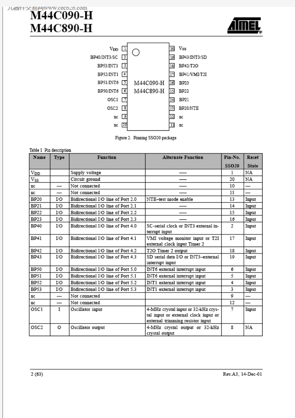
M44C890-H
M44C090-H Rev.A3, 14-Dec-01
3 (63)
Table of Contents
1Introduction 5. . . . . . . . . . . . . . . . . . . . . . . . . . . . . . . . . . . . . . . . . . . . . . . . . . . . . . . . . . . . . . . . . . . . . . 2
MARC4 Architecture 5. . . . . . . . . . . . . . . . . . . . . . . . . . . . . . . . . . . . . . . . . . . . . . . . . . . . . . . . . . . . . . 2.1General Description 5. . . . . . . . . . . . . . . . . . . . . . . . . . . . . . . . . . . . . . . . . . . . . . . . . . . . . . . . . 2.2Components of MARC4 Core 6. . . . . . . . . . . . . . . . . . . . . . . . . . . . . . . . . . . . . . . . . . . . . . . . .
2.2.1ROM 6. . . . . . . . . . . . . . . . . . . . . . . . . . . . . . . . . . . . . . . . . . . . . . . . . . . . . . . . . . . . 2.2.2RAM 6. . . . . . . . . . . . . . . . . . . . . . . . . . . . . . . . . . . . . . . . . . . . . . . . . . . . . . . . . . . . 2.2.3Registers 7. . . . . . . . . . . . . . . . . . . . . . . . . . . . . . . . . . . . . . . . . . . . . . . . . . . . . . . . . 2.2.4ALU 9. . . . . . . . . . . . . . . . . . . . . . . . . . . . . . . . . . . . . . . . . . . . . . . . . . . . . . . . . . . . . 2.2.5I/O Bus 9. . . . . . . . . . . . . . . . . . . . . . . . . . . . . . . . . . . . . . . . . . . . . . . . . . . . . . . . . . 2.2.6Instruction Set 9. . . . . . . . . . . . . . . . . . . . . . . . . . . . . . . . . . . . . . . . . . . . . . . . . . . . . 2.2.7Interrupt Structure 9. . . . . . . . . . . . . . . . . . . . . . . . . . . . . . . . . . . . . . . . . . . . . . . . . .
Software Interrupts 11. . . . . . . . . . . . . . . . . . . . . . . . . . . . . . . . . . . . . . . . . . . . . . . . . Hardware Interrupts 11. . . . . . . . . . . . . . . . . . . . . . . . . . . . . . . . . . . . . . . . . . . . . . . .
2.3Master Reset 11. . . . . . . . . . . . . . . . . . . . . . . . . . . . . . . . . . . . . . . . . . . . . . . . . . . . . . . . . . . . . . .
2.3.1Power-on Reset and Brown-out Detection 12. . . . . . . . . . . . . . . . . . . . . . . . . . . . . . . 2.3.2Watchdog Reset 13. . . . . . . . . . . . . . . . . . . . . . . . . . . . . . . . . . . . . . . . . . . . . . . . . . . 2.3.3External Clock Supervisor 13. . . . . . . . . . . . . . . . . . . . . . . . . . . . . . . . . . . . . . . . . . .
2.4V oltage Monitor 1
3. . . . . . . . . . . . . . . . . . . . . . . . . . . . . . . . . . . . . . . . . . . . . . . . . . . . . . . . . . . .
2.4.1V oltage Monitor Control / Status Register 14. . . . . . . . . . . . . . . . . . . . . . . . . . . . . . .
2.5Clock Generation 15. . . . . . . . . . . . . . . . . . . . . . . . . . . . . . . . . . . . . . . . . . . . . . . . . . . . . . . . . . .
2.5.1Clock Module 15. . . . . . . . . . . . . . . . . . . . . . . . . . . . . . . . . . . . . . . . . . . . . . . . . . . . . 2.5.2Oscillator Circuits and External Clock Input Stage 16. . . . . . . . . . . . . . . . . . . . . . . .
RC-Oscillator 1 Fully Integrated 16. . . . . . . . . . . . . . . . . . . . . . . . . . . . . . . . . . . . . . External Input Clock 16. . . . . . . . . . . . . . . . . . . . . . . . . . . . . . . . . . . . . . . . . . . . . . . . RC-Oscillator 2 with External Trimming Resistor 16. . . . . . . . . . . . . . . . . . . . . . . . . 4-MHz Oscillator 16. . . . . . . . . . . . . . . . . . . . . . . . . . . . . . . . . . . . . . . . . . . . . . . . . . 32-kHz Oscillator 17. . . . . . . . . . . . . . . . . . . . . . . . . . . . . . . . . . . . . . . . . . . . . . . . . .
2.5.3Clock Management 17. . . . . . . . . . . . . . . . . . . . . . . . . . . . . . . . . . . . . . . . . . . . . . . . .
Clock Management Register (CM)17. . . . . . . . . . . . . . . . . . . . . . . . . . . . . . . . . . . . . System Configuration Register (SC)18. . . . . . . . . . . . . . . . . . . . . . . . . . . . . . . . . . .
2.6Power-down Modes 18. . . . . . . . . . . . . . . . . . . . . . . . . . . . . . . . . . . . . . . . . . . . . . . . . . . . . . . . . . 3
Peripheral Modules 19. . . . . . . . . . . . . . . . . . . . . . . . . . . . . . . . . . . . . . . . . . . . . . . . . . . . . . . . . . . . . . . 3.1Addressing Peripherals 19. . . . . . . . . . . . . . . . . . . . . . . . . . . . . . . . . . . . . . . . . . . . . . . . . . . . . . . 3.2Bidirectional Ports 20. . . . . . . . . . . . . . . . . . . . . . . . . . . . . . . . . . . . . . . . . . . . . . . . . . . . . . . . . .
3.2.1Bidirectional Port 221. . . . . . . . . . . . . . . . . . . . . . . . . . . . . . . . . . . . . . . . . . . . . . . . .
Port 2 Data Register (P2DAT)21. . . . . . . . . . . . . . . . . . . . . . . . . . . . . . . . . . . . . . . . Port 2 Control Register (P2CR)21. . . . . . . . . . . . . . . . . . . . . . . . . . . . . . . . . . . . . . .
3.2.2Bidirectional Port 522. . . . . . . . . . . . . . . . . . . . . . . . . . . . . . . . . . . . . . . . . . . . . . . . . 3.2.3Bidirectional Port 42
4. . . . . . . . . . . . . . . . . . . . . . . . . . . . . . . . . . . . . . . . . . . . . . . . .
3.3Universal Timer/Counter / Communication Module (UTCM)25. . . . . . . . . . . . . . . . . . . . . . . .
3.3.1Timer 126. . . . . . . . . . . . . . . . . . . . . . . . . . . . . . . . . . . . . . . . . . . . . . . . . . . . . . . . . .
Timer 1 Control Register 1 (T1C1)27. . . . . . . . . . . . . . . . . . . . . . . . . . . . . . . . . . . . Timer 1 Control Register 2 (T1C2)27. . . . . . . . . . . . . . . . . . . . . . . . . . . . . . . . . . . .
元器件交易网https://www.doczj.com/doc/af5281566.html,
M44C890-H
M44C090-H Rev.A3, 14-Dec-01
4 (63)
Table of Contents (continued)
Watchdog Control Register (WDC)28. . . . . . . . . . . . . . . . . . . . . . . . . . . . . . . . . . . .
3.3.2Timer 228. . . . . . . . . . . . . . . . . . . . . . . . . . . . . . . . . . . . . . . . . . . . . . . . . . . . . . . . . .
Timer 2 Modes 29. . . . . . . . . . . . . . . . . . . . . . . . . . . . . . . . . . . . . . . . . . . . . . . . . . . . Timer 2 Output Modes 30. . . . . . . . . . . . . . . . . . . . . . . . . . . . . . . . . . . . . . . . . . . . . . Timer 2 Output Signals 31. . . . . . . . . . . . . . . . . . . . . . . . . . . . . . . . . . . . . . . . . . . . . . Timer 2 Registers 34. . . . . . . . . . . . . . . . . . . . . . . . . . . . . . . . . . . . . . . . . . . . . . . . . . Timer 2 Control Register (T2C)34. . . . . . . . . . . . . . . . . . . . . . . . . . . . . . . . . . . . . . . Timer 2 Mode Register 1 (T2M1)35. . . . . . . . . . . . . . . . . . . . . . . . . . . . . . . . . . . . . Timer 2 Mode Register 2 (T2M2)36. . . . . . . . . . . . . . . . . . . . . . . . . . . . . . . . . . . . . Timer 2 Compare and Compare Mode Registers 37. . . . . . . . . . . . . . . . . . . . . . . . . . Timer 2 Compare Mode Register (T2CM)37. . . . . . . . . . . . . . . . . . . . . . . . . . . . . . . Timer 2 COmpare Register 1 (T2CO1)37. . . . . . . . . . . . . . . . . . . . . . . . . . . . . . . . . Timer 2 COmpare Register 2 (T2CO2) Byte Write 37. . . . . . . . . . . . . . . . . . . . . . . .
3.3.3Synchronous Serial Interface (SSI)38. . . . . . . . . . . . . . . . . . . . . . . . . . . . . . . . . . . . .
SSI Peripheral Configuration 38. . . . . . . . . . . . . . . . . . . . . . . . . . . . . . . . . . . . . . . . . General SSI Operation 38. . . . . . . . . . . . . . . . . . . . . . . . . . . . . . . . . . . . . . . . . . . . . . 8-bit Synchronous Mode 39. . . . . . . . . . . . . . . . . . . . . . . . . . . . . . . . . . . . . . . . . . . . . 9-bit Shift Mode (I2C compatible)41. . . . . . . . . . . . . . . . . . . . . . . . . . . . . . . . . . . . . 8-bit Pseudo I2C Mode 42. . . . . . . . . . . . . . . . . . . . . . . . . . . . . . . . . . . . . . . . . . . . . . I2C Bus Protocol 42. . . . . . . . . . . . . . . . . . . . . . . . . . . . . . . . . . . . . . . . . . . . . . . . . . . SSI Interrupt 43. . . . . . . . . . . . . . . . . . . . . . . . . . . . . . . . . . . . . . . . . . . . . . . . . . . . . . Modulation 43. . . . . . . . . . . . . . . . . . . . . . . . . . . . . . . . . . . . . . . . . . . . . . . . . . . . . . . Internal 2-Wire Multi-Chip Link 44. . . . . . . . . . . . . . . . . . . . . . . . . . . . . . . . . . . . . . Serial Interface Registers 45. . . . . . . . . . . . . . . . . . . . . . . . . . . . . . . . . . . . . . . . . . . . Serial Interface Control Register 1 (SIC1)45. . . . . . . . . . . . . . . . . . . . . . . . . . . . . . . Serial Interface Control Register 2 (SIC2)45. . . . . . . . . . . . . . . . . . . . . . . . . . . . . . . Serial Interface Status and Control Register (SISC)46. . . . . . . . . . . . . . . . . . . . . . . Serial Transmit Buffer (STB) – Byte Write 46. . . . . . . . . . . . . . . . . . . . . . . . . . . . . . Serial Receive Buffer (SRB) – Byte Read 47. . . . . . . . . . . . . . . . . . . . . . . . . . . . . . .
3.3.4Combination Modes 47. . . . . . . . . . . . . . . . . . . . . . . . . . . . . . . . . . . . . . . . . . . . . . . .
Combination Mode Timer 2 and SSI 47. . . . . . . . . . . . . . . . . . . . . . . . . . . . . . . . . . .
4
M44C89050. . . . . . . . . . . . . . . . . . . . . . . . . . . . . . . . . . . . . . . . . . . . . . . . . . . . . . . . . . . . . . . . . . . . . . . . 4.1U505M EEPROM 50. . . . . . . . . . . . . . . . . . . . . . . . . . . . . . . . . . . . . . . . . . . . . . . . . . . . . . . . . . .
4.1.1Serial Interface 51. . . . . . . . . . . . . . . . . . . . . . . . . . . . . . . . . . . . . . . . . . . . . . . . . . . .
Serial Protocol 51. . . . . . . . . . . . . . . . . . . . . . . . . . . . . . . . . . . . . . . . . . . . . . . . . . . . .
4.1.2EEPROM 52. . . . . . . . . . . . . . . . . . . . . . . . . . . . . . . . . . . . . . . . . . . . . . . . . . . . . . . . .
EEPROM – Operating Modes 52. . . . . . . . . . . . . . . . . . . . . . . . . . . . . . . . . . . . . . . . Write Operations 52. . . . . . . . . . . . . . . . . . . . . . . . . . . . . . . . . . . . . . . . . . . . . . . . . . . Read Operations 53. . . . . . . . . . . . . . . . . . . . . . . . . . . . . . . . . . . . . . . . . . . . . . . . . . . Initialization after a Reset Condition 53. . . . . . . . . . . . . . . . . . . . . . . . . . . . . . . . . . .
5
Electrical Characteristics 54. . . . . . . . . . . . . . . . . . . . . . . . . . . . . . . . . . . . . . . . . . . . . . . . . . . . . . . . . . 5.1Absolute Maximum Ratings 54. . . . . . . . . . . . . . . . . . . . . . . . . . . . . . . . . . . . . . . . . . . . . . . . . . . 5.2DC Operating Characteristics 54. . . . . . . . . . . . . . . . . . . . . . . . . . . . . . . . . . . . . . . . . . . . . . . . . . 5.3AC Characteristics 56. . . . . . . . . . . . . . . . . . . . . . . . . . . . . . . . . . . . . . . . . . . . . . . . . . . . . . . . . . 6Package Information 61. . . . . . . . . . . . . . . . . . . . . . . . . . . . . . . . . . . . . . . . . . . . . . . . . . . . . . . . . . . . . . 7Ordering Information 62
. . . . . . . . . . . . . . . . . . . . . . . . . . . . . . . . . . . . . . . . . . . . . . . . . . . . . . . . . . . . .
元器件交易网https://www.doczj.com/doc/af5281566.html,
M44C890-H
M44C090-H Rev.A3, 14-Dec-01 5 (63)
1Introduction
The M44C090-H / M44C890-H are members of Atmels
family of 4-bit single-chip microcontrollers. They con-tain ROM, RAM, parallel I/O ports, one 8-bit
programmable multifunction timer/counter, voltage su-pervisor, interval timer with watchdog function and a sophisticated on-chip clock generation with integrated RC-, 32-kHz crystal- and 4-MHz crystal-oscillators.Table 2 provides an overview of the available variants.
2
MARC4 Architecture
2.1
General Description
The MARC4 microcontroller consists of an advanced stack-based, 4-bit CPU core and on-chip peripherals. The CPU is based on the HARV ARD architecture with physically separate program memory (ROM) and data memory (RAM). Three independent buses, the instruction bus, the memory bus and the I/O bus, are used for parallel communication between ROM, RAM and
peripherals. This enhances program execution speed by allowing both instruction prefetching, and a simultaneous communication to the on-chip peripheral circuitry. The extremely powerful integrated interrupt controller with associated eight prioritized interrupt levels supports fast and efficient processing of hardware events. The MARC4is designed for the high-level programming language qFORTH. The core includes both, an expression and a return stack. This architecture enables high-level language programming without any loss of efficiency or code density.
94 8973
Figure 3. MARC4 core
元器件交易网https://www.doczj.com/doc/af5281566.html,
M44C890-H
M44C090-H Rev.A3, 14-Dec-01
6 (63)2.2
Components of MARC4 Core
7FFFh
1FFh 000h
1F0h 1F8h 010h 018h 000h
008h 020h 1E8h 1E0h
S C A L L a d d r e s s e s
140h 180h 040h
0C0h 008h $AUTOSLEEP
$RESET
INT0
INT1INT2INT3INT4INT5INT6INT71E0h 1C0h 100h 080h
Z ero page
000h
13391
Figure 4. ROM map of M44C090-H
The core contains ROM, RAM, ALU, program counter,RAM address registers, instruction decoder and interrupt controller. The following sections describe each functional block in more detail:
2.2.1ROM
The program memory (ROM) is mask programmed with the customer application program during the fabrication of the microcontroller. The ROM is addressed by a 12–bit wide program counter, thus predefining a maximum program bank size of 2 Kbytes. An additional 1 Kbyte of ROM exists which is reserved for quality control self –test software The lowest user ROM address segment is taken up by a 512 byte zero page which contains predefined start addresses for interrupt service routines and special subroutines accessible with single byte instructions (SCALL).
The corresponding memory map is shown in figure 4.Look-up tables of constants can also be held in ROM and are accessed via the MARC4’s built-in TABLE instruction.
2.2.2RAM
The M44C090-H / M44C890-H contains 256 x 4-bit wide static random access memory (RAM). It is used for the
expression stack, the return stack and data memory for variables and arrays. The RAM is addressed by any of the four 8-bit wide RAM address registers SP, RP , X and Y .Expression Stack
The 4-bit wide expression stack is addressed with the expression stack pointer (SP). All arithmetic, I/O and memory reference operations take their operands from,and return their results to the expression stack. The MARC4 performs the operations with the top of stack items (TOS and TOS –1). The TOS register contains the top element of the expression stack and works in the same way as an accumulator. This stack is also used for passing parameters between subroutines and as a scratch pad area for temporary storage of data.Return Stack
The 12-bit wide return stack is addressed by the return stack pointer (RP). It is used for storing return addresses of subroutines, interrupt routines and for keeping loop index counts. The return stack can also be used as a temporary storage area.
The MARC4 instruction set supports the exchange of data between the top elements of the expression stack and the return stack. The two stacks within the RAM have a user definable location and maximum depth.
元器件交易网https://www.doczj.com/doc/af5281566.html,
M44C890-H
M44C090-H Rev.A3, 14-Dec-017 (63)
RAM
X Y
R A M a d d r e
s s r e g i s t e r :
(192 x 4-bit)Global variables
Expression stack
Return stack
v 13392
Figure 5. RAM map
2.2.3Registers
The MARC4 controller has seven programmable registers and one condition code register. They are shown in the following programming model.Program Counter (PC)
The program counter (PC) is a 12-bit register which contains the address of the next instruction to be fetched from the ROM. Instructions currently being executed are decoded in the instruction decoder to determine the internal micro-operations. For linear code (no calls or branches) the program counter is incremented with every instruction cycle. If a branch-, call-, return-instruction or an interrupt is executed, the program counter is loaded with a new address. The program counter is also used with the TABLE instruction to fetch 8-bit wide ROM constants.
PC
Program counter
Return stack pointer Expression stack pointer
RAM address register (X)RAM address register (Y)
Top of stack register
Condition code register
Carry / borrow
Branch Interrupt enable Reserved
Figure 6. Programming model
元器件交易网https://www.doczj.com/doc/af5281566.html,
M44C890-H
M44C090-H Rev.A3, 14-Dec-01
8 (63)RAM Address Registers
The RAM is addressed with the four 8-bit wide RAM address registers: SP, RP, X and Y. These registers allow access to any of the 256 RAM nibbles.Expression Stack Pointer (SP)
The stack pointer (SP) contains the address of the next-to-top 4-bit item (TOS –1) of the expression stack. The pointer is automatically pre-incremented if a nibble is moved onto the stack or post-decremented if a nibble is removed from the stack. Every post-decrement operation moves the item (TOS –1) to the TOS register before the SP is decremented. After a reset the stack pointer has to be initialized with ” >SP S0 ” to allocate the start address of the expression stack area.Return Stack Pointer (RP)
The return stack pointer points to the top element of the 12-bit wide return stack. The pointer automatically pre-increments if an element is moved onto the stack, or it post-decrements if an element is removed from the stack.The return stack pointer increments and decrements in steps of 4. This means that every time a 12-bit element is stacked, a 4-bit RAM location is left unwritten. This location is used by the qFORTH compiler to allocate 4-bit variables. After a reset the return stack pointer has to be initialized via ”>RP FCh ”.RAM Address Registers (X and Y)
The X and Y registers are used to address any 4-bit item in the RAM. A fetch operation moves the addressed nibble onto the TOS. A store operation moves the TOS to the addressed RAM location. By using either the pre –increment or post –decrement addressing mode arrays in the RAM can be compared, filled or moved.
Top Of Stack (TOS)
The top of stack register is the accumulator of the MARC4. All arithmetic/logic, memory reference and I/O operations use this register. The TOS register receives data from the ALU, ROM, RAM or I/O bus.Condition Code Register (CCR)
The 4-bit wide condition code register contains the branch, the carry and the interrupt enable flag. These bits indicate the current state of the CPU. The CCR flags are set or reset by ALU operations. The instructions SET_BCF, TOG_BF, CCR! and DI allow direct manipulation of the condition code register.Carry/Borrow (C)
The carry/borrow flag indicates that the borrowing or carrying out of arithmetic logic unit (ALU) occurred during the last arithmetic operation. During shift and rotate operations, this bit is used as a fifth bit. Boolean operations have no affect on the C-flag.Branch (B)
The branch flag controls the conditional program branching. Should the branch flag have been set by a previous instruction a conditional branch will cause a jump. This flag is affected by arithmetic, logic, shift, and rotate operations.Interrupt Enable (I)
The interrupt enable flag globally enables or disables the triggering of all interrupt routines with the exception of the non-maskable reset. After a reset or on executing the DI instruction, the interrupt enable flag is reset thus disabling all interrupts. The core will not accept any further interrupt requests until the interrupt enable flag has been set again by either executing an EI, RTI or SLEEP instruction.
元器件交易网https://www.doczj.com/doc/af5281566.html,
M44C890-H
M44C090-H Rev.A3, 14-Dec-019 (63)
2.2.4ALU
94 8977
Figure 7. ALU zero-address operations
The 4-bit ALU performs all the arithmetic, logical, shift
and rotate operations with the top two elements of the expression stack (TOS and TOS –1) and returns the result to the TOS. The ALU operations affect the carry/borrow and branch flag in the condition code register (CCR).
2.2.5I/O Bus
The I/O ports and the registers of the peripheral modules are I/O mapped. All communication between the core and the on-chip peripherals takes place via the I/O bus and the associated I/O control. With the MARC4 IN and OUT instructions the I/O bus allows a direct read or write access to one of the 16 primary I/O addresses. More about the I/O access to the on-chip peripherals is described in the section ”Peripheral Modules ”. The I/O bus is internal and is not accessible by the customer on the final micro-controller device, but it is used as the interface for the MARC4 emulation (see also the section ”Emulation ”).
2.2.6Instruction Set
The MARC4 instruction set is optimized for the high level programming language qFORTH. Many MARC4instructions are qFORTH words. This enables the compiler to generate a fast and compact program code.The CPU has an instruction pipeline allowing the controller to prefetch an instruction from ROM at the same time as the present instruction is being executed.
The MARC4 is a zero address machine, the instructions containing only the operation to be performed and no source or destination address fields. The operations are implicitly performed on the data placed on the stack.There are one and two byte instructions which are executed within 1 to 4 machine cycles. A MARC4machine cycle is made up of two system clock cycles (SYSCL). Most of the instructions are only one byte long and are executed in a single machine cycle. For more information refer to the ”MARC4 Programmer ’s Guide ”.
2.2.7Interrupt Structure
The MARC4 can handle interrupts with eight different priority levels. They can be generated from the internal and external interrupt sources or by a software interrupt from the CPU itself. Each interrupt level has a hard-wired priority and an associated vector for the service routine in the ROM (see table 2). The programmer can postpone the processing of interrupts by resetting the interrupt enable flag (I) in the CCR. An interrupt occurrence will still be registered, but the interrupt routine only started after the I flag is set. All interrupts can be masked, and the priority individually software configured by programming the appropriate control register of the interrupting module.(see section ”Peripheral Modules ”).
元器件交易网https://www.doczj.com/doc/af5281566.html,
M44C890-H
M44C090-H Rev.A3, 14-Dec-01
10 (63)76543210
P r i o r i t y l e v e l
Time
94 8978
Figure 8. Interrupt handling
Interrupt Processing
For processing the eight interrupt levels, the MARC4includes an interrupt controller with two 8-bit wide ”interrupt pending ” and ”interrupt active ” registers. The interrupt controller samples all interrupt requests during every non-I/O instruction cycle and latches these in the interrupt pending register. If no higher priority interrupt is present in the interrupt active register, it signals the CPU to interrupt the current program execution. If the interrupt enable bit is set, the processor enters an interrupt acknowledge cycle. During this cycle a short call (SCALL) instruction to the service routine is executed and the current PC is saved on the return stack. An interrupt service routine is completed with the RTI instruction. This instruction sets the interrupt enable flag,resets the corresponding bits in the interrupt pending/active register and fetches the return address from the return stack to the program counter. When the interrupt enable flag is reset (triggering of interrupt routines are disabled), the execution of new interrupt
service routines is inhibited but not the logging of the interrupt requests in the interrupt pending register. The execution of the interrupt is delayed until the interrupt enable flag is set again. Note that interrupts are only lost if an interrupt request occurs while the corresponding bit in the pending register is still set (i.e., the interrupt service routine is not yet finished).
It should also be noted that automatic stacking of the RBR is not carried out by the hardware and so if ROM banking is used, the RBR must be stacked on the expression stack by the application program and restored before the RTI.After a master reset (power-on, brown-out or watchdog reset), the interrupt enable flag and the interrupt pending and interrupt active register are all reset.Interrupt Latency
The interrupt latency is the time from the occurrence of the interrupt to the interrupt service routine being activated. In MARC4 this is extremely short (taking between 3 to 5 machine cycles depending on the state of the core).
元器件交易网https://www.doczj.com/doc/af5281566.html,
M44C890-H
M44C090-H Rev.A3, 14-Dec-0111 (63)
Software Interrupts
The programmer can generate interrupts by using the software interrupt instruction (SWI) which is supported in qFORTH by predefined macros named SWI0...SWI7.The software triggered interrupt operates exactly like any hardware triggered interrupt. The SWI instruction takes the top two elements from the expression stack and writes the corresponding bits via the I/O bus to the interrupt pending register. Therefore, by using the SWI instruction,interrupts can be re-prioritized or lower priority processes scheduled for later execution.
Hardware Interrupts
In the M44C090-H, there are eleven hardware interrupt sources with seven different levels. Each source can be masked individually by mask bits in the corresponding control registers. An overview of the possible hardware configurations is shown in table 4.
2.3Master Reset
The master reset forces the CPU into a well-defined condition. It is unmaskable and is activated independent of the current program state. It can be triggered by either initial supply power-up, a short collapse of the power sup-ply, brown-out detection circuitry, watchdog time-out, or an external input clock supervisor stage (see figure 9). A master reset activation will reset the interrupt enable flag,the interrupt pending register and the interrupt active register. During the power-on reset phase the I/O bus con-trol signals are set to ’reset mode ’ thereby initializing all on-chip peripherals. All bidirectional ports are set to input mode. Attention: During any reset phase, the BP20/NTE input is driven towards V DD by a strong pull-up transistor.Releasing the reset results in a short call instruction (opcode C1h) to the ROM address 008h. This activates the initialization routine $RESET which in turn has to initialize all necessary RAM variables, stack pointers and peripheral configuration registers (see table 7).
元器件交易网https://www.doczj.com/doc/af5281566.html,
M44C890-H
M44C090-H Rev.A3, 14-Dec-01
12 (63)
V reset
DD SS DD SS 13752
Figure 9. Reset configuration
2.3.1
Power-on Reset and Brown-out Detection
The M44C090-H / M44C890-H has a fully integrated power-on reset and brown-out detection circuitry. For re-set generation no external components are needed .These circuits ensure that the core is held in the reset state until the minimum operating supply voltage has been
reached. A reset condition will also be generated should the supply voltage drop momentarily below the minimum operating level except when a power down mode is activated (the core is in SLEEP mode and the peripheral clock is stopped). In this power-down mode the brown-out detection is disabled.
Two values for the brown-out voltage threshold are
programmable via the BOT-bit in the SC-register.
V t d = 1.5 ms (typically)
13753
BOT = 1, low brown-out voltage threshold. (1.7 V) is reset value.BOT = 0, high brown-out voltage threshold (1.9 V).
Figure 10. Brown-out detection
元器件交易网https://www.doczj.com/doc/af5281566.html,
M44C890-H
M44C090-H Rev.A3, 14-Dec-0113 (63)
A power-on reset pulse is generated by a V DD rise across the default BOT voltage level (1.7 V). A brown-out reset pulse is generated when V DD falls below the brown-out voltage threshold. Two values for the brown-out voltage threshold are programmable via the BOT-bit in the SC-register. When the controller runs in the upper supply voltage range with a high system clock frequency, the high threshold must be used. When it runs with a lower system clock frequency, the low threshold and a wider supply voltage range may be chosen. For further details,see the electrical specification and the SC-register description for BOT programming.
2.3.2Watchdog Reset
The watchdog ’s function can be enabled at the WDC-reg-ister and triggers a reset with every watchdog counter overflow. To supress the watchdog reset, the watchdog counter must be regularly reset by reading the watchdog register address (CWD).
The CPU reacts in exactly the same manner as a reset stimulus from any of the above sources.
2.3.3External Clock Supervisor
The external input clock supervisor function can be enabled if the external input clock is selected within the CM- and SC-registers of the clock module.
The CPU reacts in exactly the same manner as a reset stimulus from any of the above sources.
2.4
Voltage Monitor
The voltage monitor consists of a comparator with internal voltage reference. It is used to supervise the supply voltage or an external voltage at the VMI-pin. The comparator for the supply voltage has three internal programmable thresholds one lower threshold (2.2 V),one middle threshold (2.6 V). and one higher threshold (3.0 V). For external voltages at the VMI-pin, the comparator threshold is set to V BG = 1.3 V . The VMS-bit indicates if the supervised voltage is below (VMS = 0) or above (VMS = 1) this threshold. An interrupt can be generated when the VMS-bit is set or reset to detect a rising or falling slope. A voltage monitor interrupt (INT7)is enabled when the interrupt mask bit (VIM) is reset in the VMC-register.
BP41/VMI
Figure 11. V oltage monitor
元器件交易网https://www.doczj.com/doc/af5281566.html,
M44C890-H
M44C090-H Rev.A3, 14-Dec-01
14 (63)2.4.1
Voltage Monitor Control / Status Register
Primary register address: ’F ’hex
VM2:V oltage monitor M ode bit 2VM1:V oltage monitor M ode bit 1VM0:V oltage monitor M ode bit 0
VIM V oltage I nterrupt M ask bit
VIM = 0, voltage monitor interrupt is enabled VIM = 1, voltage monitor interrupt is disabled VMS V oltage M onitor S tatus bit
VMS = 0, the voltage at the comparator input is below Vref
VMS = 1, the voltage at the comparator input is above Vref
V 13755
Figure 12. Internal supply voltage supervisor
13756
Figure 13. External input voltage supervisor
元器件交易网https://www.doczj.com/doc/af5281566.html,
M44C890-H
M44C090-H Rev.A3, 14-Dec-0115 (63)
2.5
Clock Generation
2.5.1
Clock Module
The M44C090-H / M44C890-H contains a clock module with 4 different internal oscillator types: two RC-oscillators, one 4-MHz crystal oscillator and one 32-kHz crystal oscillator. The pins OSC1 and OSC2 are the interface to connect a crystal either to the 4-MHz, or to the 32-kHz crystal oscillator. OSC1 can be used as input for external clocks or to connect an external trimming resistor for the RC-oscillator 2. All necessary circuitry except the crystal and the trimming resistor is integrated on-chip. One of these oscillator types or an external input clock can be selected to generate the system clock (SYSCL).
In applications that do not require exact timing, it is possible to use the fully integrated RC-oscillator 1without any external components. The RC-oscillator 1center frequency tolerance is better than ±50%. The RC-oscillator 2 is a trimmable oscillator whereby the oscillator frequency can be trimmed with an external resistor attached between OSC1 and V DD . In this
configuration, the RC-oscillator 2 frequency can be maintained stable to within a tolerance of ±15% over the full operating temperature and voltage range.
The clock module is programmable via software with the clock management register (CM) and the system configuration register (SC). The required oscillator configuration can be selected with the OS1-bit and the OS0-bit in the SC-register. A programmable 4-bit divider stage allows the adjustment of the system clock speed. A special feature of the clock management is that an external oscillator may be used and switched on and off via a port pin for the power-down mode. Before the external clock is switched off, the internal RC-oscillator 1 must be selected with the CCS-bit and then the SLEEP mode may be activated. In this state an interrupt can wake up the controller with the RC-oscillator, and the external oscillator can be activated and selected by software. A synchronization stage avoids too short clock periods if the clock source or the clock speed is changed. If an external input clock is selected, a supervisor circuit monitors the external input and generates a hardware reset if the external clock source fails or drops below 500 kHz for more than 1 msec.
Figure 14. Clock module
元器件交易网https://www.doczj.com/doc/af5281566.html,
M44C890-H
M44C090-H Rev.A3, 14-Dec-01
16 (63)The clock module generates two output clocks. One is the system clock (SYSCL) and the other the periphery (SUBCL). The SYSCL can supply the core and the peripherals and the SUBCL can supply only the peripherals with clocks. The modes for clock sources are programmable with the OS1-bit and OS0-bit in the SC-register and the CCS-bit in the CM-register.
2.5.2
Oscillator Circuits and External Clock Input Stage
The M44C090-H / M44C890-H series consists of four dif-ferent internal oscillators: two RC-oscillators, one 4-MHz crystal oscillator, one 32-kHz crystal oscillator and one external clock input stage.
RC-Oscillator 1 Fully Integrated
For timing insensitive applications, it is possible to use
the fully integrated RC oscillator 1. It operates without any external components and saves additional costs. The RC –oscillator 1 center frequency tolerance is better than ±50% over the full temperature and voltage range. The basic center frequency of the RC-oscillator 1 is f O [3.8 MHz The RC oscillator 1 is selected by default after power –on reset.
Figure 15. RC-oscillator 1
External Input Clock
The OSC1 can be driven by an external clock source provided it meets the specified duty cycle, rise and fall times and input levels. Additionally the external clock stage contains a supervisory circuit for the input clock.The supervisor function is controlled via the OS1,OS0-bit in the SC –register and the CCS –bit in the CM-register. If the external input clock fails and CCS = 0 is set in the CM-register, the supervisory circuit generates a hardware reset. The input clock has failed if the frequency is less than 500 kHz for more than 1 ms.
Figure 16. External input clock
RC-Oscillator 2 with External Trimming Resistor
The RC-oscillator 2 is a high resolution trimmable oscillator whereby the oscillator frequency can be trimmed with an external resistor between OSC1 and V DD . In this configuration, the RC-oscillator 2 frequency can be maintained stable to within a tolerance of ±10%over the full operating temperature and, voltage range from V DD = 2.5 V to 6V.
For example: An output frequency at the RC-oscillator 2of 2 MHz, can be obtained by connecting a resistor R ext = 360 k ? (see figure 17).
Figure 17. RC-oscillator 2
4-MHz Oscillator
The M44C090-H / M44C890-H 4-MHz oscillator options need a crystal or ceramic resonator connected to the OSC1 and OSC2 pins to establish oscillation. All the necessary oscillator circuitry, with the exception of the actual crystal, resonator, C3 and C4 are integrated on-chip.
元器件交易网https://www.doczj.com/doc/af5281566.html,
M44C890-H
M44C090-H Rev.A3, 14-Dec-0117 (63)
Figure 18. 4-MHz crystal oscillator
C2 = C3 = 22 pF
Figure 19. Ceramic resonator
32-kHz Oscillator
Some applications require long-term time keeping or low resolution timing. In this case, an on –chip, low power 32-kHz crystal oscillator can be used to generate both the SUBCL and the SYSCL. In this mode, power consumption is greatly reduced. The 32-kHz crystal oscillator can not be stopped while the power-down mode is in operation.
Figure 20. 32-kHz crystal oscillator
2.5.3Clock Management
The clock management register controls the system clock divider and synchronization stage. Writing to this register triggers the synchronization cycle.
Clock Management Register (CM)
Auxiliary register address: ’3’hex
Bit 3Bit 2Bit 1Bit 0CM:
NSTOP
CCS
CSS1
CSS0
Reset value: 1111b
NSTOP
N ot STOP peripheral clock
NSTOP = 0, stops the peripheral clock while the core is in SLEEP mode NSTOP = 1, enables the peripheral clock while the core is in SLEEP mode CCS
C ore C lock S elect
CCS = 1, the internal RC-oscillator 1 generates SYSCL
CCS = 0, the 4-MHz crystal oscillator, the 32-kHz crystal oscillator, an external clock source or the internal RC-oscillator 2 with the external resistor at OSC1 generates SYSCL dependent on the set-ting of OS0 and OS1 in the system configuration register CSS1C ore S peed S elect 1CSS0
C ore S peed S elect 0
元器件交易网https://www.doczj.com/doc/af5281566.html,
M44C890-H
M44C090-H Rev.A3, 14-Dec-01
18 (63)System Configuration Register (SC)
Primary register address: ’3’hex
BOT
B rown-O ut T hreshold
BOT = 1, low brown-out voltage threshold (1.7 V)BOT = 0, high brown-out voltage threshold (2.0 V)OS1O scillator S elect 1OS0
O scillator S elect 0
If the bit CCS = 0 in the CM-register the RC-oscillator 1 always stops.
2.6Power-down Modes
The sleep mode is a shut-down condition which is used to reduce the average system power consumption in applica-tions where the μC is not fully utilized. In this mode, the system clock is stopped. The sleep mode is entered via the SLEEP instruction. This instruction sets the interrupt en-able bit (I) in the condition code register to enable all interrupts and stops the core. During the sleep mode the peripheral modules remain active and are able to generate interrupts. The μC exits the sleep mode by carrying out any interrupt or a reset.
The sleep mode can only be kept when none of the inter-rupt pending or active register bits are set. The application of the $AUTOSLEEP routine ensures the correct function of the sleep mode. For standard applications use the $AU-TOSLEEP routine to enter the power-down mode. Using the SLEEP instruction instead of the $AUTOSLEEP fol-lowing an I/O instruction requires to insert 3 non I/O
instruction cycles (for example NOP NOP NOP) between the IN or OUT command and the SLEEP command.The total power consumption is directly proportional to the active time of the μC. For a rough estimation of the expected average system current consumption, the fol-lowing formula should be used:
I total (V DD ,f syscl ) = I Sleep + (I DD t active / t total )I DD depends on V DD and f syscl .
The M44C090-H / M44C890-H has various power-down modes. During the sleep mode the clock for the MARC4core is stopped. With the NSTOP-bit in the clock manage-ment register (CM) it is programmable if the clock for the on –chip peripherals is active or stopped during the sleep mode. If the clock for the core and the peripherals is stopped the selected oscillator is switched off. An excep-tion is the 32-kHz oscillator, if it is selected it runs continously independent of the NSTOP-bit. If the oscilla-tor is stopped or the 32 kHz oscillator is selected, power consumption is extremely low.Table 6 Power-down modes
* Osc-Stop = SLEEP & NSTOP & WDL
元器件交易网https://www.doczj.com/doc/af5281566.html,
M44C890-H
M44C090-H Rev.A3, 14-Dec-0119 (63)
3
Peripheral Modules
3.1
Addressing Peripherals
Accessing the peripheral modules takes place via the I/O bus (see figure 21). The IN or OUT instructions allow di-rect addressing of up to 16 I/O modules. A dual register addressing scheme has been adopted to enable direct ad-dressing of the ”primary register ”. To address the ”auxiliary register ”, the access must be switched with an ”auxiliary switching module ”. Thus a single IN (or OUT)
primary register. Accessing the auxiliary register is per-formed with the same instruction preceded by writing the module address into the auxiliary switching module. Byte wide registers are accessed by multiple IN- (or OUT-)instructions. For more complex peripheral modules, with a larger number of registers, extended addressing is used.In this case a bank of up to 16 subport registers are indi-rectly addressed with the subport address. The first OUT-instruction writes the subport address to the sub-address register, the second IN- or OUT-instruction reads data from or writes data to the addressed subport.Addr.(Mx) = Module Mx Address Aux._Data = data to be written into Auxiliary Register
Prim._Data = data to be written into Primary Register.
Addr.(ASW) = Auxiliary Switch Module Address SPort_Data(lo) = data to be written into SubP ort (low nibble)SPort_Data(hi) = data to be written into Subport (high nibble)Addr.(SPort) = Subport Address
Aux._Data (lo )= data to be written into Auxiliar y Re g ister (low nibble )
Aux._Data (hi) = data to be written into Auxiliary Register(high nibble)13357
(lo) = SPort_Data (low nibble)(hi) = SPort_Data (high nibble)
Figure 21. Example of I/O addressing
元器件交易网https://www.doczj.com/doc/af5281566.html,
M44C890-H
M44C090-H Rev.A3, 14-Dec-01
20 (63)
Table 7 Peripheral addresses
3.2Bidirectional Ports
All ports (2, 4 and 5) are 4 bits wide. All ports may be used for data input or output. All ports are equipped with Schmitt trigger inputs and a variety of mask options for open drain, open source, full complementary outputs, pull up and pull down transistors. All Port Data Registers (PxDA T) are I/O mapped to the primary address register of the respective port address and the Port Control Regis-ter (PxCR), to the corresponding auxiliary register.There are three different directional ports available:Port 24-bit wide bitwise-programmable I/O port.
Port 54-bit wide bitwise-programmable bidirectional
port with optional strong pull-ups and program-mable interrupt logic.Port 44-bit wide bitwise-programmable bidirectional
port also provides the I/O interface to Timer 2,SSI, voltage monitor input and external interrupt input.
元器件交易网https://www.doczj.com/doc/af5281566.html,