General Description
The MAX1823 is a dual, current-limited switch with autoreset specifically made for USB applications. The autoreset feature latches the switch off if the output is shorted, saving system power. The switch reactivates when the short circuit is removed. Each channel is guar-anteed to supply 720mA and meet USB specifications.Low quiescent supply current (50μA) and standby current (3μA) conserve battery power in portable applications.The MAX1823 has multiple safety features to ensure that the USB port is protected. Built-in thermal-overload protection limits power dissipation and junction temper-ature. Accurate internal current-limiting circuitry pro-tects the input supply against both overload and short-circuit conditions. Independent fault signals (FAULTA and FAULTB ) notify the microprocessor (μP)when a thermal-overload, current-limit, undervoltage-lockout (UVLO), or short-circuit fault occurs. A 20ms fault-blanking feature ignores momentary faults, such as those caused when hot swapping a capacitive load,preventing false alarms to the host system. The MAX1823A/MAX1823B also block reverse current (cur-rent from OUT_ to IN_) while in shutdown.
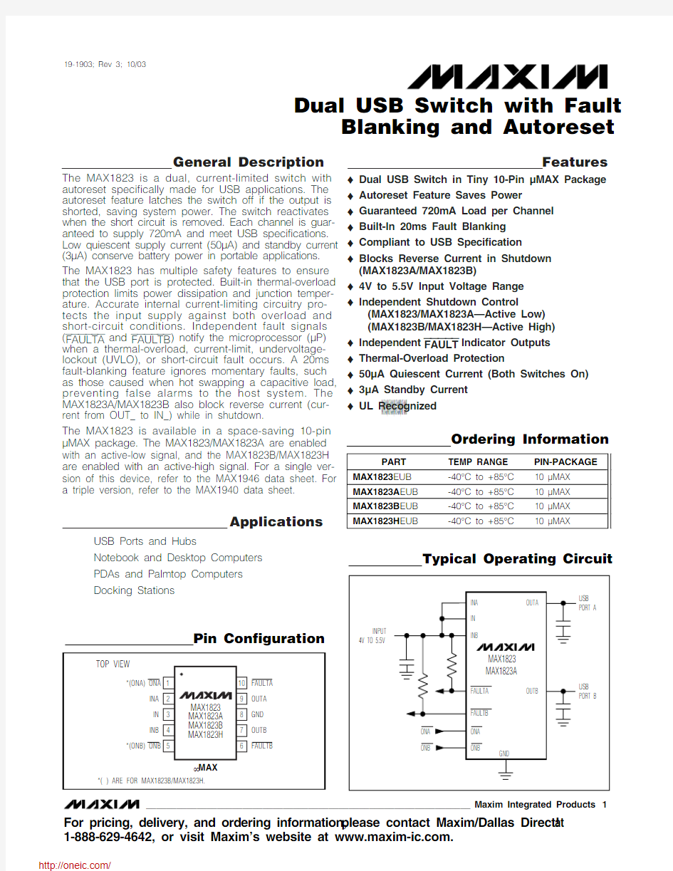
The MAX1823 is available in a space-saving 10-pin μMAX package. The MAX1823/MAX1823A are enabled with an active-low signal, and the MAX1823B/MAX1823H are enabled with an active-high signal. For a single ver-sion of this device, refer to the MAX1946 data sheet. For a triple version, refer to the MAX1940 data sheet.
Applications
USB Ports and Hubs
Notebook and Desktop Computers PDAs and Palmtop Computers Docking Stations
Features
o Dual USB Switch in Tiny 10-Pin μMAX Package
o Autoreset Feature Saves Power o Guaranteed 720mA Load per Channel o Built-In 20ms Fault Blanking o Compliant to USB Specification o Blocks Reverse Current in Shutdown (MAX1823A/MAX1823B)o 4V to 5.5V Input Voltage Range o Independent Shutdown Control
(MAX1823/MAX1823A—Active Low)(MAX1823B/MAX1823H—Active High)o Independent FAULT Indicator Outputs o Thermal-Overload Protection
o 50μA Quiescent Current (Both Switches On)o 3μA Standby Current o UL Recognized
MAX1823/MAX1823A/MAX1823B/MAX1823H
Dual USB Switch with Fault
Blanking and Autoreset
________________________________________________________________Maxim Integrated Products 1
Ordering Information
Typical Operating Circuit
19-1903; Rev 3; 10/03
Pin Configuration
For pricing, delivery, and ordering information,please contact Maxim/Dallas Direct!at 1-888-629-4642, or visit Maxim’s website at https://www.doczj.com/doc/af3088097.html,.
M A X 1823/M A X 1823A /M A X 1823B /M A X 1823H
Dual USB Switch with Fault Blanking and Autoreset 2_______________________________________________________________________________________
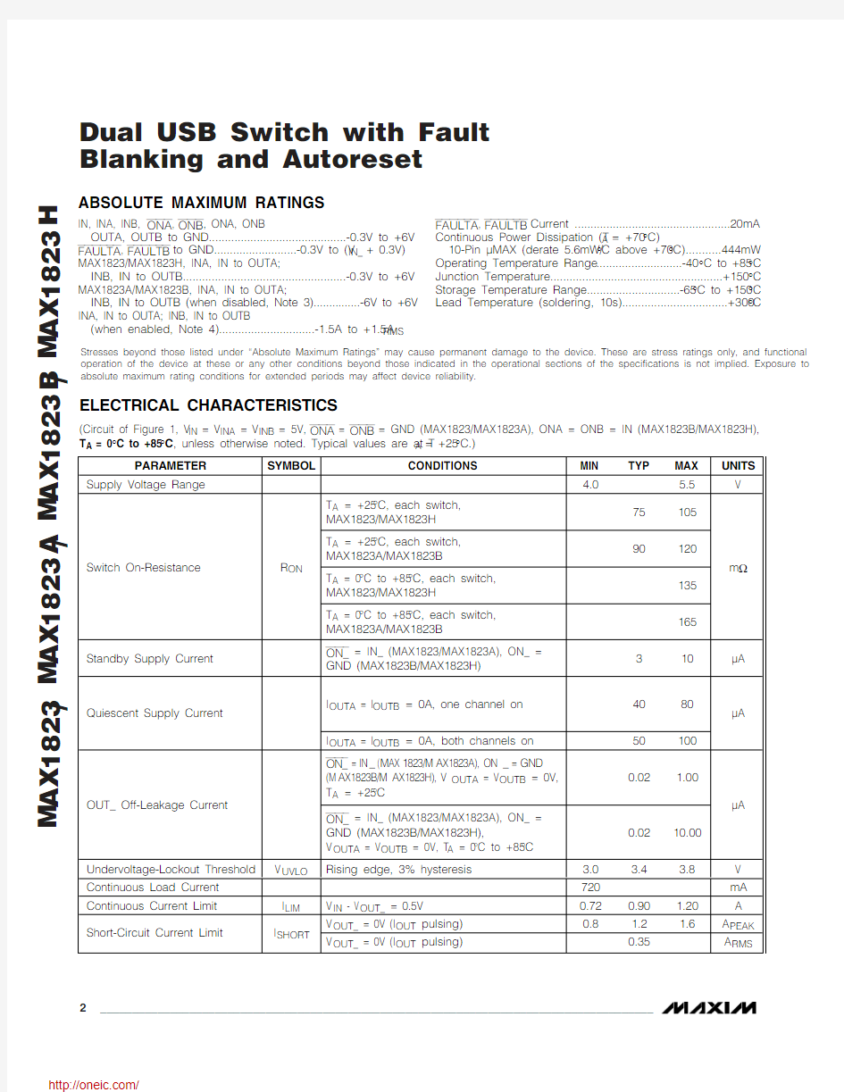
ABSOLUTE MAXIMUM RATINGS
Stresses beyond those listed under “Absolute Maximum Ratings” may cause permanent damage to the device. These are stress ratings only, and functional operation of the device at these or any other conditions beyond those indicated in the operational sections of the specifications is not implied. Exposure to absolute maximum rating conditions for extended periods may affect device reliability.
IN, INA, INB, ONA , ONB , ONA, ONB
OUTA, OUTB to GND...........................................-0.3V to +6V FAULTA , FAULTB to GND..........................-0.3V to (V IN_+ 0.3V)MAX1823/MAX1823H, INA, IN to OUTA;
INB, IN to OUTB...................................................-0.3V to +6V MAX1823A/MAX1823B, INA, IN to OUTA;
INB, IN to OUTB (when disabled, Note 3)...............-6V to +6V INA, IN to OUTA; INB, IN to OUTB
(when enabled, Note 4)..............................-1.5A to +1.5A RMS
FAULTA , FAULTB Current .................................................20mA Continuous Power Dissipation (T A = +70°C)
10-Pin μMAX (derate 5.6mW/°C above +70°C)...........444mW Operating Temperature Range ...........................-40°C to +85°C Junction Temperature......................................................+150°C Storage Temperature Range.............................-65°C to +150°C Lead Temperature (soldering, 10s).................................+300°C
ELECTRICAL CHARACTERISTICS
(Circuit of Figure 1, V IN = V INA = V INB = 5V, ONA = ONB = GND (MAX1823/MAX1823A), ONA = ONB = IN (MAX1823B/MAX1823H), T A = 0°C to +85°C , unless otherwise noted. Typical values are at T A = +25°C.)
ELECTRICAL CHARACTERISTICS (continued)
MAX1823/MAX1823A/MAX1823B/MAX1823H Dual USB Switch with Fault Blanking and Autoreset (Circuit of Figure 1, V IN= V INA= V INB= 5V, ONA= ONB= GND (MAX1823/MAX1823A), ONA = ONB = IN (MAX1823B/MAX1823H),
T A = 0°C to +85°C, unless otherwise noted. Typical values are at T A= +25°C.) Array
_______________________________________________________________________________________3
M A X 1823/M A X 1823A /M A X 1823B /M A X 1823H
Dual USB Switch with Fault Blanking and Autoreset 4_______________________________________________________________________________________
ELECTRICAL CHARACTERISTICS
(Circuit of Figure 1, V IN = V IN _ = V ON _ = 5V (MAX1823B/MAX1823H); V IN = V IN _ = 5V, ON_ = GND (MAX1823/MAX1823A), T A = -40°C to +85°C , unless otherwise noted.) (Note 2)
MAX1823/MAX1823A/MAX1823B/MAX1823H
Dual USB Switch with Fault
Blanking and Autoreset
_______________________________________________________________________________________5
ELECTRICAL CHARACTERISTICS (continued)
(Circuit of Figure 1, V IN = V IN _ = V ON _ = 5V (MAX1823B/MAX1823H); V IN = V IN _ = 5V, ON_ = GND (MAX1823/MAX1823A), T A = -40°C to +85°C , unless otherwise noted.) (Note 2)
Note 2:Specifications to -40°C are guaranteed by design, not production tested.Note 3:Reverse current (current from OUT_ to IN_) is blocked when disabled.
Note 4:Forward current (current from IN_ to OUT_) is internally limited. Reverse current, from OUT_ to IN_, is not limited when the
device is enabled and must be kept below 1.5A RMS to prevent permanent device damage. When the MAX1823A/MAX1823B are disabled, the switch turns off and reverse current is internally blocked.
Typical Operating Characteristics
(Circuit of Figure 1, V IN = V INA = V INB = 5V, ON _=GND (MAX1823/MAX1823A), ON_ = IN_ (MAX1823B/MAX1823H), T A = +25°C,unless otherwise noted.)
018126243036424854600
2
1
3
4
5
6
QUIESCENT CURRENT vs. INPUT VOLTAGE
M A X 1823 t o c 01
INPUT VOLTAGE (V)
Q U I E S C E N T C U R R E N T (μA )
454751
49
53
55
-40
10
-15
35
60
85
QUIESCENT CURRENT vs. TEMPERATURE
TEMPERATURE (°C)
Q U I E S C E N T
C U R R E N T (μA )
2.52.7
3.1
2.9
3.3
3.5-40
10
-15
35
60
85
SHUTDOWN SUPPLY CURRENT
vs. TEMPERATURE
TEMPERATURE (°C)
S H U T D O W N S U P P L Y C U R R E N T (μA )
M A X 1823/M A X 1823A /M A X 1823B /M A X 1823H
Dual USB Switch with Fault Blanking and Autoreset 6_______________________________________________________________________________________
940930
920
910
900
-40
10
-15
35
60
85
TEMPERATURE (°C)
C O N T I N U O U S C U R R E N T L I M I T (m A )
CONTINUOUS CURRENT-LIMIT THRESHOLD vs. TEMPERATURE
0.01
0.1101
100
1000-40
10
-15
35
60
85
SWITCH OFF-LEAKAGE vs. TEMPERATURE
M A X 1823 t o c 04
TEMPERATURE (°C)
S W I T C H O F F -L E A K A G E (n A )
1.501.25
1.000.750.50
-40
10
-15
35
60
85
NORMALIZED R ON vs. TEMPERATURE
M A X 1823 t o c 05
TEMPERATURE (°C)
N O R M A L I Z E D R O N
3.03.2
3.6
3.4
3.8
4.0-40
10
-15
35
60
85
TURN-ON TIME
vs. TEMPERATURE (t ON + t RISE )
TEMPERATURE (°C)
T U R N -O N T I M E (m s )
2.5
2.7
3.1
2.9
3.33.5-40
10
-15
35
60
85
TURN-OFF TIME
vs. TEMPERATURE (t OFF + t FALL )
TEMPERATURE (°C)
T U R N -O F F T I M E (m s )
21.0
21.2
21.6
21.4
21.8
22.0
-40
10
-15
35
60
85
FAULT-BLANKING TIME vs. TEMPERATURE
TEMPERATURE (°C)
F A U L T -B L A N K I N
G T I M E (m s )
0.100
0.1500.1250.200
0.1750.2250.250
-40
10
-15
35
60
85
FAULT_ OUTPUT LOW VOLTAGE
vs. TEMPERATURE
TEMPERATURE (°C)F A U L T _ O U T P U T L O W V O L T A G E (V )
15
20
30
25
35
40
-40
10
-15
356085AUTORESET CURRENT vs. TEMPERATURE
(MAX1823/MAX1823H)
TEMPERATURE (°C)A U T O R E S E T C U R R E N T (m A )
28
30
32
34
36
-4010-15356085
AUTORESET CURRENT vs. TEMPERATURE
(MAX1823A/MAX1823B)
TEMPERATURE (°C)
A U T O R E S E T C U R R E N T (m A )
Typical Operating Characteristics (continued)
(Circuit of Figure 1, V IN = V INA = V INB = 5V, ON _=GND (MAX1823/MAX1823A), ON_ = IN_ (MAX1823B/MAX1823H), T A = +25°C,unless otherwise noted.)
MAX1823/MAX1823A/MAX1823B/MAX1823H
Dual USB Switch with Fault
Blanking and Autoreset
_______________________________________________________________________________________7
010
30
20
40
50
INPUT VOLTAGE (V)
A U T O R E S E T C U R R E N T (m A )
3.6
5.2
4.4
6.0
AUTORESET CURRENT vs. INPUT VOLTAGE
(MAX1823/MAX1823H)
25
27293335313739
INPUT VOLTAGE (V)
A U T O R E S E T C U R R E N
T (m A )
3.6
5.2
4.4
6.0
AUTORESET CURRENT vs. INPUT VOLTAGE
(MAX1823A/MAX1823B)
10ms/div
OVERLOAD RESPONSE INTO 2.5?
(MAX1823/MAX1823H)
A: V IN_, 5V/div B: V OUTA
, 5V/div
C: V FAULTA , 5V/div D: I OUTA , 1A/div
A
B
D
C
MAX1823 toc15
5V
10ms/div
OVERLOAD RESPONSE INTO 2.5?(MAX1823A/MAX1823B ONLY)
A: V IN_, 5V/div B: V OUTA
, 5V/div
C: V FAULTA , 5V/div D: I OUTA , 1A/div
A
B
D
C
MAX1823 toc16
5V
500μs/div
OVERLOAD RESPONSE INTO 2.5?
(EXPANDED TIME SCALE)
A: V
IN_, 5V/div B: V OUTA , 5V/div
A B
D
C
MAX1823 toc17
5V
C: V FAULTA , 5V/div D: I OUTA , 1A/div
10ms/div
SHORT-CIRCUIT RESPONSE INTO 0?
(MAX1823/MAX1823H)
A B
D
C
MAX1823 toc18
5V
C: V FAULTA , 5V/div D: I OUTA , 1A/div
A: V IN _, 5V/div B: V OUTA , 5V/div
10ms/div
SHORT-CIRCUIT RESPONSE INTO 0?
(MAX1823A/MAX1823B)
A B
D
C
MAX1823 toc19
5V
C: V FAULTA , 5V/div D: I OUTA , 2A/div
A: V IN _, 5V/div B: V OUTA , 5V/div 500μs/div
SHORT-CIRCUIT RESPONSE INTO 0?
(EXPANDED TIME SCALE)
A: V IN_, 5V/div B: V OUTA , 5V/div
A
B D
C
MAX1823 toc20
5V
5V
0C: V FAULTA , 5V/div D: I OUTA , 2A/div
1ms/div
SWITCH TURN-ON TIME (MAX1823/MAX1823A)
A: V ONA , 5V/div B: V OUTA , 2V/div
A
B
MAX1823 toc21
Typical Operating Characteristics (continued)
(Circuit of Figure 1, V IN = V INA = V INB = 5V, ON _=GND (MAX1823/MAX1823A), ON_ = IN_ (MAX1823B/MAX1823H), T A = +25°C,unless otherwise noted.)
M A X 1823/M A X 1823A /M A X 1823B /M A X 1823H
Dual USB Switch with Fault Blanking and Autoreset 8_______________________________________________________________________________________
Pin Description
1ms/div
SWITCH TURN-OFF TIME
(t OFF + t FALL )
A: V ONA , 5V/div B: V OUTA , 2V/div
A
B
MAX1823 toc22
500μs/div
STARTUP TIME
(TYPICAL USB APPLICATION)
A: V ONA , 5V/div B: V FAULTA , 5V/div A
B
MAX1823 toc23
5V
C
D
0C: V OUTA , 2V/div D : I OUTA , 0.5A/div
Typical Operating Characteristics (continued)
(Circuit of Figure 1, V IN = V INA = V INB = 5V, ON _=GND (MAX1823/MAX1823A), ON_ = IN_ (MAX1823B/MAX1823H), T A = +25°C,unless otherwise noted.)
Detailed Description The MAX1823 is a dual, current-limited switch designed for USB applications. It has two independent switches, each with its own enable control input and autoreset function. Each switch has an error-flag output to notify the USB controller when the current-limit, short-circuit, undervoltage-lockout, or thermal-shutdown threshold is reached (Figure 2).
The MAX1823 operates from a 4V to 5.5V input voltage range and guarantees a minimum 720mA output current.
A built-in 0.9A current limit limits the current in the event of a heavy-overload condition. The MAX1823 has inde-pendent thermal shutdown for each switch in the event of a prolonged overload or short-circuit condition. The autoreset function monitors the overload and automati-cally turns the switch on when the overload is removed. Use of low-R ON NMOS switches enables the MAX1823 to provide two switches in the ultra-small 10-pin μMAX package. An internal micropower charge pump gener-ates the high-side supply needed for driving the gates of these high-side switches. Separate current-limiting and thermal-shutdown circuits permit each switch to operate independently, improving system robustness.
Undervoltage-Lockout and
Input-Voltage Requirements The MAX1823 includes a UVLO circuit to prevent erro-neous switch operation when the input voltage goes low during startup and brownout conditions. Operation is inhibited when V IN_is less than 3.4V.
Output Fault Protection The MAX1823 senses the switch output voltage and selects continuous current limiting when V OUT is greater than 1V or short-circuit current limiting when V OUT is less than 1V. When V OUT is greater than 1V, the device oper-ates in a continuous current-limit mode that sets the out-put current limit to 0.9A. When V OUT is less than 1V, the device operates in short-circuit current-limit mode, sourcing 0.35A RMS current pulses to the load.
Autoreset Mode If an output fault is detected for more than the 20ms blanking time, the output latches off, the FAULT_output goes low, and a 25mA current is forced at the output. If the voltage on the output exceeds 0.5V for 20ms, the fault resets, the 25mA current source shuts down, and the out-put turns on. The device monitors the output voltage so that a short-circuit condition can be detected. Active loads are not expected to have measurable currents when the supply is below 0.5V. The MAX1823/MAX1823A can also be reset from fault manually by toggling ON_ (ON_ for the MAX1823B/MAX1823H) for that channel.
Thermal Shutdown The MAX1823 features independent thermal shutdown for each switch channel, allowing one switch to deliver power even if the other switch has a fault condition. When the junction temperature exceeds +160°C, the switch turns off and the FAULT_output goes low imme-diately; fault blanking does not occur during thermal limit. When the junction cools by 15°C, the switch turns on again. If the fault overload condition continues, the switch cycles on and off, resulting in a pulsed output, saving battery power.
Reverse Current Blocking The USB specification does not allow an output device to source current back into the USB port. However, the MAX1823A/MAX1823B are designed to safely power noncompliant devices. When disabled, each output is switched to a high-impedance state, blocking reverse current flow from the output back to the input. However, during normal operation with the device enabled, the MAX1823A/MAX1823B are bidirectional switches.
Fault Indicators The MAX1823 provides an open-drain fault output (FAULT_) for each switch. For most applications, connect FAULT_to IN_through a 100k?pullup resistor. FAULT_ goes low when any of the following conditions occur:
?The input voltage is below the UVLO threshold.?The switch junction temperature exceeds the +160°C thermal-shutdown temperature limit.
?The switch is in current-limit or short-circuit limit mode after the fault-blanking period is exceeded.?The switch is in autoreset mode.
Figure 1. Typical Application Circuit
MAX1823/MAX1823A/MAX1823B/MAX1823H Dual USB Switch with Fault Blanking and Autoreset
_______________________________________________________________________________________9
M A X 1823/M A X 1823A /M A X 1823B /M A X 1823H
Dual USB Switch with Fault Blanking and Autoreset 10
______________________________________________________________________________________
After the fault condition is removed, the FAULT_output deasserts after a 20ms delay. Ensure that the MAX1823has adequate input bypass capacitance to prevent glitches from triggering FAULT_outputs. Input glitches greater than 0.2V/μs may cause erroneous FAULT_indications.
Behavior During Current Limit
and Fault Blanking
The MAX1823 limits switch current in three ways. When ON_ is deasserted (high for MAX1823/MAX1823A, low for MAX1823B/MAX1823H), the switch is off and leak-age dominates the residual output current. When ON_is asserted (low for MAX1823/MAX1823A, high for MAX1823B/MAX1823H), the switch supplies a continu-ous output current of at least 720mA. When the output current exceeds the 0.9A threshold, the MAX1823 lim-its the current depending on the output voltage. F or V OUT_greater than 1V (current-limit mode), the MAX1823 regulates the output current to 0.9A. F or
V OUT_less than 1V (short-circuit mode), the MAX1823pulses the switch, decreasing the current to 0.35A RMS (Table 1). Note that a thermal overload may result from either of these high-current conditions.
The MAX1823 switches may enter current limit in nor-mal operation when powering up or driving heavy capacitive loads. To differentiate these conditions from short circuits or sustained overloads that may damage the device, the MAX1823 has an independent fault-blanking circuit in each switch. When a load transient causes the device to enter current limit, an internal counter starts to monitor the duration of the fault. F or load faults exceeding 20ms fault-blanking time, the switch turns off, the FAULT_signal asserts low, and the device enters autoreset mode (see the Autoreset Mode section). Only current-limit and short-circuit faults are blanked. Thermal-overload faults and input voltage drops below the UVLO threshold immediately cause the switch to turn off and FAULT_to assert low.
Figure 2. Functional Diagram
分销商库存信息:
MAXIM
MAX1823BEUB+T MAX1823AEUB+T MAX1823AEUB+ MAX1823BEUB+MAX1823HEUB+MAX1823HEUB+T MAX1823EUB+MAX1823EUB+T