InN p-i-n Nanowire Solar Cells on Si Hieu Pham Trung Nguyen,Yi-Lu Chang,Ishiang Shih,and Zetian Mi
(Invited Paper)
Abstract—In this paper,we report the?rst experimental demon-stration of InN nanowire solar cells.By employing an in situ de-posited In seeding layer,we have achieved electronically pure, nearly intrinsic InN nanowires directly on Si(111)substrates by molecular beam epitaxy.The growth and characterization of Si-and Mg-doped InN nanowires is also investigated,which can ex-hibit superior structural and optical properties.We have further studied the epitaxial growth,fabrication,and characterization of InN:Si/i-InN and InN:Mg/i-InN/InN:Si axial nanowire structures on p-type and n-type Si(111)substrates,respectively.With the use of a CdS surface passivation,InN:Mg/i-InN/InN:Si nanowire homojunction solar cells exhibit a promising short-circuit cur-rent density of~14.4mA/cm2and power-conversion ef?ciency of~0.68%under simulated one-sun(AM1.5G)illumination.This work suggests the?rst successful demonstration of p-type doping in InN nanowires and also constitutes important progress for the development of InGaN-based,full-solar-spectrum photovoltaics.
Index Terms—Nanotechnology,optoelectronic devices,p-i-n diodes,solar cells.
I.I NTRODUCTION
S INCE the recent discovery of InN bandgap at~0.6to
0.7eV,the use of InN and related alloys for solar-cell appli-cations has been proposed and intensively investigated[1]–[9]. InN also exhibits several important attributes,including a rel-atively high absorption coef?cient,high carrier mobility,and large drift velocity that are required for high-ef?ciency pho-tovoltaics.An energy-conversion ef?ciency of over20%is ex-pected for an ideal InN single-junction solar cell[10].Addition-ally,InN may be integrated with Si or other thin?lms to form heterojunction solar cells or be incorporated as a critical subcell for future InGaN-based full-solar-spectrum multijunction de-vices[11].However,InN thin?lms generally exhibit extremely poor quality,due to the lack of suitable substrates,and,to date, an InN solar cell has not been demonstrated.It is therefore imperative to explore InN nanostructures,including nanowires and quantum dots,which can exhibit drastically reduced dis-location densities,owning to the highly effective lateral stress relaxation.Additional advantages offered by the1-D nanowires for solar-cell applications include a direct path for carrier trans-port,an increased surface area for enhanced light absorption,
Manuscript received July13,2010;revised August10,2010;accepted August10,2010.Date of publication November11,2010;date of current ver-sion August5,2011.This work was supported in part by the Natural Sciences and Engineering Research Council of Canada and in part by the Hydro-Quebec Nano-Engineering Scholar Program at McGill University.
The authors are with the Department of Electrical and Computer Engi-neering,McGill University,Montreal,QC H3A2A7,Canada(e-mail:zetian. mi@mcgill.ca).
Digital Object Identi?er10.1109/JSTQE.2010.2082505and the compatibility with Si or other low-cost,large-area sub-strates[12]–[14].
The growth and characterization of InN nanowires have been intensively studied.InN nanowires can be formed using the vapor–liquid–solid growth process,the spontaneous formation under nitrogen-rich conditions,or the selective-area growth on nano-patterned substrates[15]–[17].Well-spaced,vertically aligned InN nanowires have been grown on Si and other sub-strates using plasma-assisted molecular beam epitaxy(MBE) or metal–organic chemical vapor deposition.The resulting InN nanowires generally exhibit a wurtzite crystal structure,with the growth direction oriented along the c-axis.However,due to the very low dissociation temperature of InN and the very high surface migration rate of In,conventional growth techniques yield InN nanowires with tapered surface morphology and large stacking fault and dislocation densities[18]–[20],which de-crease the carrier diffusion length and severely limit the solar cell ef?ciency.The wires also exhibit very large size dispersion, with signi?cant variations in the diameters and heights.Addi-tionally,due to the extremely low conduction band minimum of InN,any defects,dislocations or impurities generally form donors,thereby leading to very high electron densities,which are commonly measured in the range of~1×1018cm?3,or higher for nominally nondoped InN[20]–[25].The resulting n-type degenerate InN nanowires exhibit poor optical properties, characterized by nearly temperature and power invariant pho-toluminescence emission spectra and photoluminescence peak energies(~0.7to0.8eV)considerably larger than the bandgap of InN[20],[21],[26].The uncontrolled structural,electrical and optical properties have posed a signi?cant challenge for the rational design and fabrication of InN nanowire solar cells. The realization of InN nanowire solar cells,as well as many other semiconductor devices,has been further limited by the dif?culty in achieving p-type doping.In this regard,Mg-doped InN?lms and the formation of p-type carriers have been in-vestigated both theoretically and experimentally[27]–[30].A Fermi level shift toward the valence band was measured in InN:Mg layers[30],and the possibility of p-type doping is further suggested by electrolyte capacitance-voltage measure-ments[28],[31].Free-to-acceptor photoluminescence emission has also been observed in Mg-doped InN,with an activation energy of~61meV derived for the Mg acceptor[29].In order to compensate the presence of large electron densities of nom-inally nondoped InN as well as the associated surface electron accumulation,a relatively high concentration of Mg dopant is required,which,however,may lead to the formation Mg-related, donorlike defects[29],[32],[33].Additionally,the growth and characterization of InN:Mg nanowires,to the best of our knowl-edge,has not been reported.It has been observed that the
1077-260X/$26.00?2010IEEE
incorporation of Mg can signi?cantly affect the formation and structural properties of GaN nanowires[34],[35].The presence of Mg can greatly reduce the nanowire nucleation time and en-hance the growth rate on the nonpolar surfaces,thereby leading to wires with increased diameters and reduced lengths.Deterio-rated crystal structures were further observed at relatively high Mg concentrations.
It is therefore of tremendous importance to develop nearly intrinsic InN nanowires as well as InN nanowire p-n junctions, in order to exploit the full potential of InN for third generation photovoltaics.In this context,we have performed a detailed in-vestigation of the MBE growth and characterization of nearly intrinsic and Si-and Mg-doped InN nanowires on Si(111) substrates without any external metal catalyst.Under optimized growth conditions,the wires exhibit nontapered surface mor-phology and excellent structural and optical properties.An ex-tremely narrow spectral linewidth of~8meV,compared to the commonly reported values of50–100meV for n-type degener-ate InN nanowires,have been achieved for nearly intrinsic InN nanowires.Effects of Si and Mg incorporation on the structural and optical properties of InN nanowires have also been investi-gated.We have further studied the epitaxial growth,fabrication, and characterization of InN:Si/i-InN and InN:Mg/i-InN/InN:Si nanowire axial structures on p-type and n-type Si(111)sub-strates,respectively.With the use of CdS surface passivation, InN:Mg/i-InN/InN:Si nanowire homojunction solar cells exhibit a promising short-circuit current density of~14.4mA/cm2and power-conversion ef?ciency of~0.68%under simulated one-sun(AM1.5G)illumination.In Section II,the MBE growth and characterization of nearly intrinsic and Si-and Mg-doped InN nanowires is?rst presented.In Section III,we describe the design and fabrication of InN nanowire solar cells monolith-ically grown on Si.The characterization results and analysis are presented in Section IV.Finally,conclusions are made in Section V.
II.MBE G ROWTH AND C HARACTERIZATION
OF I N N N ANOWIRES
A.Nearly Intrinsic InN Nanowires on Si Substrates Electronically pure InN nanowires were grown on Si(111) substrates by plasma-assisted MBE under nitrogen-rich con-ditions without any external metal catalyst.To achieve high-quality InN nanowires with controllable structural properties, we investigated the self-catalytic growth of InN nanowires.In this process,a thin(~0.5to1.6nm)In seeding layer is?rst deposited on the Si substrate surface prior to growth initia-tion[36],[37].The thin In layer forms nanoscale liquid droplets at elevated temperatures,which provides well-de?ned nucle-ation centers for the formation and growth of InN nanowires. Subsequently,the InN nanowire growth is carried out at a nom-inal growth rate of0.6?A/s,nitrogen?ow rate of1.0–2.0sccm, growth temperature of440–520?C,and RF plasma forward power of~400W.
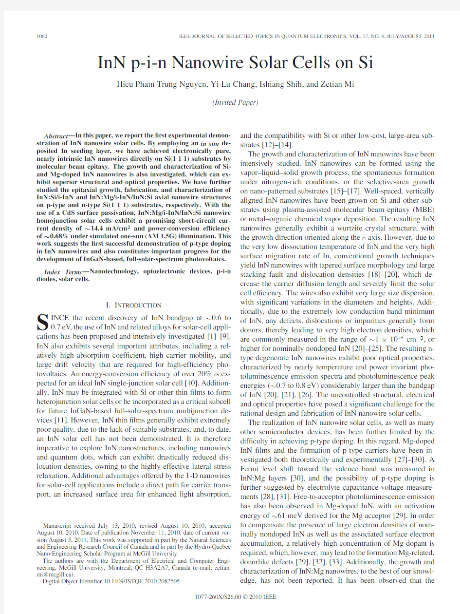
The scanning electron micrographs of InN nanowires grown on Si without and with the use of In seeding layer are shown in Fig.1(a)and(b),respectively.It is evident that signi?cantly improved structural properties,with a nontapered surface
mor-Fig.1.Scanning electron micrographs of nondoped InN nanowires grown on Si(111)substrates by MBE(a)without and(b)with the use of an in situ deposited In seeding layer.
phology and nearly identical heights,can be obtained by using an in situ deposited In seeding layer.Detailed analysis,described elsewhere[36],further con?rms that the wires have a wurtzite crystal structure,orient along the c-axis and are relatively free of dislocations.
Important for practical device applications is a precise control of the carrier concentration and conductivity of InN nanowires. The residual electron density of InN can be derived from a Hall-effect measurement or by analyzing the photoluminescence spectral linewidth measured at low temperatures[38],[39].For conventional n-type degenerate InN,the measured photolumi-nescence linewidths are generally in the range of50–100meV, which correspond to residual electron densities of~1018cm?3, or higher[21].Illustrated in Fig.2are the photoluminescence spectra for the presently achieved nontapered InN nanowires measured under various laser powers at5K.An extremely narrow spectral linewidth of8meV was obtained under low excitation conditions.Detailed analysis revealed that the elec-tron density in the undoped InN nanowires is~2×1015cm?3, or less,which is nearly a factor of500times smaller than the commonly reported values[20]–[25],suggesting,for the?rst time,the achievement of nearly intrinsic InN.The presence of an extremely low level of carrier concentration in the undoped InN nanowires is also directly re?ected in the power-dependent photoluminescence emission,as shown in Fig.2.With increas-ing excitation power,there is a considerable blueshift in the photoluminescence peak energy,accompanied by a signi?cant
Fig.2.Photoluminescence spectra of nondoped InN nanowires on Si(111)measured at 5K under various laser
powers.
Fig.3.Photoluminescence spectra of InN nanowires on Si(111)substrates for Si doping concentrations of ~1×1018cm ?3(dashed and dotted line),2×1017cm ?3(dotted line),5×1016cm ?3(dashed line),nondoped (solid line),measured at 5K.
broadening of the spectral linewidth.Such a clear band-?lling effect has not been previously observed in the photolumines-cence emission of n-type degenerate InN.B.Si and Mg-Doped InN Nanowires
With the achievement of nearly intrinsic InN nanowires,we have subsequently investigated the growth and optical proper-ties of Si-and Mg-doped InN nanowires.These nanowires are grown by introducing the respective dopants during nanowire growth without any modi?cations to the previously described growth conditions.Due to the signi?cantly enhanced In adatom surface migration and the preferred growth along the nanowire length direction,the resulting doping level is generally smaller,compared to that of planar heterostructures.It is expected that the local dopant ?uctuation in the wires may also be negligible,due to the relatively large (>100nm)wire diameters.For the Si doping concentrations considered (<~1×1018cm ?3),no morphological changes to the InN nanowires were observed.However,the incorporation of Si dopant can signi?cantly mod-ify the optical properties of InN nanowires.
Illustrated in Fig.3are the photoluminescence spectra of InN:Si nanowires measured at 5K for various Si doping lev-els.It is seen that,with increasing Si doping concentration,InN nanowires exhibit a considerable blueshift in the photolumines-cence peak energy,a drastic increase in the spectral linewidth,and a signi?cant decrease in the luminescence ef?ciency.
Such
Fig.4.Scanning electron microscopy image of InN nanowires grown on Si(111)substrates with a relatively high Mg doping concentration.The wires show deteriorated structural properties,with the presence of slightly tapered surface morphology.
effects have also been observed at elevated temperatures and under various laser powers.The observed Burstein–Moss shift,i.e.,the signi?cant increase in the photoluminescence peak en-ergy and broadening of the spectral linewidth,can be well ex-plained by the increased electron densities with increasing Si doping concentrations.However,the exact origin of the drasti-cally reduced luminescence ef?ciency with increasing Si doping concentration remains unclear.One possible explanation is the increasing surface electron accumulation,induced by the bulk electron density that leads to a signi?cantly increased spatial separation of charge carriers in the wires.As a consequence,the radiative ef?ciency is reduced with increasing Si doping concentration.The correlation between the surface charge ac-cumulation and the bulk electron density has been suggested by recent studies [22].Detailed discussions on the surface charge properties of nearly intrinsic and Si-doped InN nanowires are described elsewhere.
From photoluminescence measurements of InN:Mg ?lms,it was determined that the Mg acceptor activation energy was about 61meV [29].However,to the best of our knowledge,the growth and properties of InN:Mg nanowires have not been reported.In this study,InN:Mg nanowires,with Mg effusion cell temperatures varying from 185?C to 235?C,are grown and characterized.It was observed that,for relatively low Mg concentrations,InN nanowires with excellent surface morphol-ogy and structural properties can be obtained.However,with increasing Mg ?ux,the wires show increasing diameter and re-ducing length,potentially due to the reduced adatom surface migration.Similar effects have also been observed for GaN:Mg nanowires [34],[35].A further increase of the Mg concentration generally leads to a tapered surface morphology,as shown in Fig.4,and the generation of dislocations.
Illustrated in Fig.5are the photoluminescence spectra of InN:Mg nanowires measured at 5K for various Mg effu-sion cell temperatures.It is observed that the photolumines-cence peak intensity decreases considerably with increasing Mg
Fig.5.5K photoluminescence spectra of InN:Mg nanowires grown at differ-ent Mg effusion cell temperatures.
incorporation,which may be directly related to the formation of Mg-related defects.A detailed investigation of the underly-ing mechanism as well as the electrical transport properties and p-type conductivity of InN:Mg wires will be published in the future.
III.D ESIGN AND F ABRICATION OF I N N
N ANOWIRE S OLAR C ELLS ON S I
Three InN nanowire solar cell designs,schematically illus-trated in Fig.6(a)–(c),have been investigated.In the?rst ap-proach,as shown in Fig.6(a),the InN nanowire solar cells consist of~0.3μm nondoped and0.4μm Si-doped sections, which are grown directly on p-type Si(111)substrates.Such a design does not require the use of p-type InN nanowires,which had not been demonstrated prior to this study.The second and third designs employ InN p-i-n axial homojunctions,illustrated in Fig.6(b)and(c),which comprise of~0.8μm InN:Si,0.2μm nondoped InN,and0.3μm InN:Mg sections grown on n-type Si(111)https://www.doczj.com/doc/9115145298.html,pared to the?rst design,the p-n junc-tion is formed within the wires.It may be noted that there is a small variation in the thicknesses of the device intrinsic regions, which may not have any major impact on the device ef?ciency. One of the primary limitations for semiconductor nanowire devices is the signi?cant nonradiative carrier recombination as-sociated with the presence of surface states,which can be greatly minimized by using core–shell or dot/well-in-a-wire nanoscale heterostructures[40],[41].In this regard,we have further inves-tigated the use of a CdS passivation technique in the third design. Illustrated in Fig.6(c),a thin(~10nm)CdS layer is coated on the nanowire surface using a chemical bath deposition method at~70?C,wherein the bath consists of CdCl2,NH4Cl,and NH4OH,with a molecular proportion of2:20:20:200[42].The resulting CdS layer is nearly intrinsic and exhibits a very high resistivity(~106Ω·cm)[43].Such a passivation/buffer layer has been widely used in the fabrication of CuIn(Ga)Se2solar cells and has led to the most ef?cient(~19.9%)thin?lm solar cells ever reported[44].Growth conditions for the various nanowire samples have been carefully controlled to achieve high-quality InN nanowires with relatively large diameters(>150nm)to effectively enhance the light absorption[45].
The fabrication process for InN nanowire solar cells on Si is brie?y described for the second design.A polyimide(PI)
resist Fig.6.Schematic illustrations of(a)InN:Si/i-InN nanowire solar cells grown on p-type Si substrates,(b)InN:Mg/i-InN/InN:Si nanowire solar cells grown on n-type Si substrates,and(c)CdS-passivated InN:Mg/i-InN/InN:Si nanowire solar cells grown on n-type Si substrates.The top contact consists of thin (~15nm)Ni/Au or Ti/Au layers.
layer is?rst spin-coated to fully cover the InN nanowires for surface planarization.The PI layer is subsequently etched using O2:CF4(1:4)dry-etching until the top region of the wires is exposed,as shown in Fig.7(a).The sample is then?ood-exposed with UV light and hard-baked at350?C for~30min to cure the PI.The top exposed section of the wires is patterned,using standard photolithography,into cells of various sizes(0.09–1.00mm2)and,a thin Ni/Au(5nm/10nm)p-metal contact is deposited on the cell surface,as shown in Fig.7(b),which is followed by the deposition of thick Ni/Au metal contact layers at the periphery of the devices.Ti/Au(30nm/150nm)layers are then deposited on the backside of the n-Si substrate as the n-metal contact.The sample is annealed at300–400?C for60s.
IV.R ESULTS AND D ISCUSSSIONS
The performance characteristics of InN nanowire solar cells on Si is measured under dark and illuminated(one sun at AM 1.5G)conditions.Characteristics of the?rst design,i.e.,the InN:Si/i-InN/p-Si heterojunction nanowire solar cells is?rst
Fig.7.45?scanning electron microscopy images of(a)the InN nanowire ensemble spin-coated with a PI layer,with the top region of the wires exposed by dry etching and(b)the PI immersed wire ensemble after the deposition of Ni/Au contact layers.
described.The current–voltage(I–V)response of such devices measured under dark conditions is shown in Fig.8(a).It is seen that InN/Si nanowire heterojunction design exhibits very poor diode characteristics,with rectifying ratios in the range of~2 to4measured at?0.5and0.5V.At?1V,a leakage current of more than100mA/cm2was measured.As a consequence,no signi?cant photo response was observed.The measured short-circuit current density and energy-conversion ef?ciency are less than2mA/cm2and0.01%,respectively.The underlying mech-anism for the extremely poor device performance has been in-vestigated.Due to the very large electron af?nity(~5.8eV) of InN,its conduction band minimum is positioned well below the valence band maximum of Si.In addition,a thin(~2to 3nm)amorphous layer(SiN x)is generally formed at the InN/Si mis?t interface[36].The resulting energy-band diagram of the n-InN/i-InN/p-Si heterostructure under thermal equilibrium is schematically shown in Fig.8(b).The depletion occurs at both sides of the InN/Si junction.It is seen that large densities of electrons accumulate at the InN/Si junction interface,which can readily recombine with holes in the Si valence band and therefore explains the quasi-ohmic behavior observed for the n-InN/i-InN/p-Si heterojunction device under dark conditions. However,the depletion creates a signi?cant barrier to the trans-port of photogenerated holes,leading to negligible response under
illumination.Fig.8.(a)I–V response of InN:Si/i-InN nanowire devices on p-Si(111) measured under dark conditions.(b)Schematic of the energy band diagram of the InN:Si/i-InN/p-Si heterojunction under thermal equilibrium.The presence of a thin(~2to3nm)amorphous SiN x layer is also
illustrated.
Fig.9.(a)I–V characteristics of InN:Mg/i-InN/InN:Si nanowire solar cells grown on n-type Si(111)substrates under dark and illumination(1-sun at AM 1.5G)conditions.(b)Illustration of the corresponding energy band diagram of the nanowire junction under thermal equilibrium.
Drastically improved device performance,illustrated in Fig.9(a),has been measured for the second solar cell de-sign grown on n-type Si substrates.Under dark conditions,the InN:Si/i-InN/InN:Mg nanowire device exhibits characteristics of a diode structure,with a signi?cantly improved rectifying ratio(~60)measured at–1and+1V,which is attributed to the built-in electric?eld in the p-i-n nanowire homojunction.
Fig.10.I–V characteristics of CdS-passivated InN:Mg/i-InN/InN:Si nanowire solar cells grown on n-type Si(111)substrates under dark and light (1-sun at AM1.5G)illumination conditions.
In addition,a clear photoresponse has been consistently ob-served.Under simulated AM1.5G illumination,a promising short-circuit current density of~12.91mA/cm2is obtained for a device area of1mm2.The measured open-circuit voltage,?ll factor,and power-conversion ef?ciency are~0.13V,30.2%, and0.51%,respectively.The functioning of the InN p-i-n axial homojunction solar cells on n-type Si may be explained by the energy-band diagram under thermal equilibrium.Illustrated in Fig.9(b),it may be noted that the depletion region widths of the InN/Si junction are small,due to the very high doping concen-trations in InN and Si.As a consequence,electrons can readily tunnel from InN to Si.Illumination from the top of the nanowires would result in photons with energy larger than E g(InN)to be absorbed by the nanowires.The holes and electrons produced in InN can be promptly collected by the ohmic contacts at the top of the wires and the back contact of the substrate,respectively, thereby generating the observed photocurrent.While photons with energy larger than E g(Si)could also be absorbed by the substrate when light illuminates onto the Si surface through the gap between the wires,the contribution to the photocurrent is expected to be negligible,due to the presence of a signi?cant barrier to hole transport across the InN/Si heterointerface. The performance of the afore-described InN:Si/i-InN/ InN:Mg nanowire homojunction solar cells may be severely lim-ited by the presence of surface states,which can be addressed,to a certain extent,with the use of CdS surface passivation[46].Il-lustrated in Fig.10are the measured I–V curves under dark and illuminated conditions for the third nanowire solar cell design, wherein a thin(~10nm)CdS passivation layer is incorporated.
A reduction in the reverse leakage current and an improvement in the rectifying ratio(~150)were measured,compared to iden-tical devices fabricated without the use of any CdS passivation. The improved diode characteristics are attributed to the effec-tive carrier con?nement provided by the large bandgap CdS and the suppression of carrier leakage through the wire surface.Un-der one-sun(AM1.5G)illumination,the devices exhibit further improved performance,with a short-circuit current density of ~14.4mA/cm2,open-circuit voltage of0.14V,?ll factor of 34.0%,and energy-conversion ef?ciency of0.68%.It may be noted that the measured short-circuit current densities are much larger than the commonly reported values for nanowire solar cells[12],[13],[47]–[49].The open-circuit voltage,however,is relatively low,which can be improved by utilizing large bandgap InGaN nanowires and by optimizing the surface passivation and fabrication processes.
The performance of the presently demonstrated InN nanowire solar cells may also be severely limited by the surface electron accumulation of n-type InN and the nonideal carrier transport across the InN/Si mis?t interface,due to the presence of an amorphous SiN x layer.Improved device performance is,there-fore,expected by utilizing core/shell heterostructures and by employing a planar GaN or InN buffer layer.Additionally,the energy-conversion ef?ciency is practically limited by the very low wire density in this experiment.Shown in Fig.7(a),the sur-face coverage of InN nanowires is less than30%.As a result,a signi?cant portion of the solar radiation cannot be absorbed by InN,and the bene?t of light trapping associated with nanowires may be absent as well.Consequently,by optimizing the wire density and diameters,the energy-conversion ef?ciency can be readily increased by a factor of3,or larger.More importantly, the energy-conversion ef?ciency is expected to improve substan-tially for InGaN nanowire solar cells with an optimized energy bandgap.The use of coalescent growth for a planar top contact layer will also greatly facilitate the device fabrication and re-duce the series resistance[50].The growth and characterization of high-performance InGaN nanowire solar cells on Si,with the use of optimized surface passivation and device fabrication processes,are being investigated.
V.C ONCLUSION
In summary,we have investigated the MBE growth and char-acterization of high quality InN nanowires on Si(111)substrates and achieved nearly intrinsic InN nanowires as well as Si-and Mg-doped InN nanowires with excellent morphological and op-tical properties.We have further demonstrated the?rst InN solar cells,consisting of InN:Si/i-InN/InN:Mg nanowire homojunc-tions on n-type Si(111)substrates,which exhibit a promising short-circuit current density of~14.4mA/cm2and an energy-conversion ef?ciency of~0.68%under one-sun(AM1.5G) illumination.Further improvement in the device performance is being investigated by optimizing the growth and fabrication processes.The present work constitutes important progress for the realization of InGaN-based third generation solar cells.It has also mitigated some of the major barriers for the future develop-ment of InN-based nanoelectronic and nanophotonic devices.
A CKNOWLEDGMENT
Part of the work was performed in the McGill Nanotools Microfab Laboratory.
R EFERENCES
[1]J.Wu,W.Walukiewicz,K.M.Yu,W.Shan,J.W.Ager,E.E.Haller,H.Lu,
W.J.Schaff,W.K.Metzger,and S.Kurtz,“Superior radiation resistance of In1?x Ga x N alloys:Full-solar-spectrum photovoltaic material system,”
J.Appl.Phys.,vol.94,pp.6477–6482,Nov.15,2003.
[2]O.Jani,I.Ferguson,C.Honsberg,and S.Kurtz,“Design and characteri-
zation of GaN/InGaN solar cells,”Appl.Phys.Lett.,vol.91,pp.132117-1–1132117-3,Sep.24,2007.
[3]H.Hamzaoui,A.S.Bouazzi,and B.Rezig,“Theoretical possibilities of
In x Ga1?x N tandem PV structures,”Sol.Energ.Mat.Sol.Cells.,vol.87, pp.595–603,May2005.
[4]X.M.Cai,S.W.Zeng,and B.P.Zhang,“Fabrication and characterization
of InGaN p-i-n homojunction solar cell,”Appl.Phys.Lett.,vol.95, pp.173504-1–173504-3,Oct.26,2009.
[5]L.Hsu and W.Walukiewicz,“Modeling of InGaN/Si tandem solar cells,”
J.Appl.Phys.,vol.104,pp.024507-1–024507-7,Jul.15,2008.
[6]J.Wu,W.Walukiewicz,W.Shan,K.Yu,J.Ager,S.Li,E.Haller,H.Lu,
and W.Schaff,“Temperature dependence of the fundamental band gap of InN,”J.Appl.Phys.,vol.94,pp.4457–4460,Oct.1,2003.
[7] C.Neufeld,N.Toledo,S.Cruz,M.Iza,S.DenBaars,and U.Mishra,“High
quantum ef?ciency InGaN/GaN solar cells with2.95eV band gap,”Appl.
Phys.Lett.,vol.93,pp.143502-1–143502-3,Oct.6,2008.
[8] E.Trybus,G.Namkoong,W.Henderson,S.Burnham,W.Doolittle,
M.Cheung,and A.Cartwright,“InN:A material with photovoltaic promise and challenges,”J.Cryst.Growth,vol.288,pp.218–224,Mar.
1,2006.
[9]X.B.Zhang,X.L.Wang,H.L.Xiao,C.B.Yang,J.X.Ran,C.M.Wang,
Q.F.Hou,J.M.Li,and Z.G.Wang,“Theoretical design and performance of In x Ga1?x N two-junction solar cells,”J.Phys.D:Appl.Phys.,vol.41, p.245104,Dec.21,2008.
[10] C.H.Henry,“Limiting ef?ciencies of ideal single and multiple energy
gap terrestrial solar cells,”J.Appl.Phys.,vol.51,pp.4494–4500,Aug.
1980.
[11]H.Neff,O.Semchinova,A.Lima,A.Fillmonov,and G.Holzhueter,
“Photovoltaic properties and technological aspects of In1?x Ga x N/Si,Ge (0 [12]Y.Tang,Z.Chen,H.Song,C.Lee,H.Cong,H.Cheng,W.Zhang, I.Bello,and S.Lee,“Vertically aligned p-type single-crystalline GaN nanorod arrays on n-type Si for heterojunction photovoltaic cells,”Nano Lett.,vol.8,pp.4191–4195,Dec.2008. [13]Y.J.Dong,B.Z.Tian,T.J.Kempa,and C.M.Lieber,“Coaxial group III-nitride nanowire photovoltaics,”Nano Lett.,vol.9,pp.2183–2187, May2009. [14]K.H.Yu and J.H.Chen,“Enhancing solar cell ef?ciencies through1-D nanostructures,”Nanoscale Res.Lett.,vol.4,pp.1–10,Jan.2009. [15]Z.Cai,S.Garzon,M.Chandrashekhar,R.Webb,and G.Koley,“Synthesis and properties of high-quality InN nanowires and nanonetworks,”J. Electron.Mater.,vol.37,pp.585–592,May2008. [16] C.Chao,J.Chyi,C.Hsiao,C.Kei,S.Kuo,H.Chang,and T.Hsu,“Catalyst- free growth of indium nitride nanorods by chemical-beam epitaxy,”Appl. Phys.Lett.,vol.88,pp.233111-1–233111-3,Jun.5,2006. [17] C.Liang,L.Chen,J.Hwang,K.Chen,Y.Hung,and Y.Chen,“Selective- area growth of indium nitride nanowires on gold-patterned Si(100)sub-strates,”Appl.Phys.Lett.,vol.81,pp.22–24,Jul.1,2002. [18]T.Stoica,R.Meijers,R.Calarco,T.Richter,and H.Luth,“MBE growth optimization of InN nanowires,”J.Cryst.Growth,vol.290,pp.241–247, Apr.15,2006. [19]J.Grandal,M.Sanchez-Garcia,E.Calleja,E.Luna,and A.Trampert,“Ac- commodation mechanism of InN nanocolumns grown on Si(111)sub-strates by molecular beam epitaxy,”Appl.Phys.Lett.,vol.91,pp.021902-1–021902-3,Jul.9,2007. [20]J.Segura-Ruiz,N.Garro,A.Cantarero,C.Denker,J.Malindretos,and A.Rizzi,“Optical studies of MBE-grown InN nanocolumns:Evidence of surface electron accumulation,”Phys.Rev.B,vol.79,pp.115305-1–115305-9,Mar.2009. [21]T.Stoica,R.Meijers,R.Calarco,T.Richter,E.Sutter,and H.Luth,“Pho- toluminescence and intrinsic properties of MBE-grown InN nanowires,” Nano Lett.,vol.6,pp.1541–1547,Jul.12,2006. [22]V.Darakchieva,T.Hofmann,M.Schubert,B.E.Sernelius,B.Monemar, P.O.A.Persson,F.Giuliani,E.Alves,H.Lu,and W.J.Schaff,“Free electron behavior in InN:On the role of dislocations and surface electron accumulation,”Appl.Phys.Lett.,vol.94,pp.022109-1–022109-3,Jan. 12,2009. [23]M.Feneberg,J.Daubler,K.Thonke,R.Sauer,P.Schley,and R. Goldhahn,“Mahan excitons in degenerate wurtzite InN:Photolumines-cence spectroscopy and re?ectivity measurements,”Phys.Rev.B,vol.77, pp.245207-1–245207-6,Jun.2008. [24] A.Janotti and C.G.Van de Walle,“Sources of unintentional conductivity in InN,”Appl.Phys.Lett.,vol.92,pp.032104-1–032104-3,Jan.21,2008.[25] C.G.Van de Walle and J.Neugebauer,“Universal alignment of hydrogen levels in semiconductors,insulators and solutions,”Nature,vol.423, pp.626–628,Jun.5,2003. [26] E.Calleja,J.Grandal,M.Sanchez-Garcia,M.Niebelschutz,V.Cimalla, and O.Ambacher,“Evidence of electron accumulation at nonpolar sur-faces of InN nanocolumns,”Appl.Phys.Lett.,vol.90,pp.262110-1–262110-3,Jun.25,2007. [27]J.H.Song,T.Akiyama,and A.J.Freeman,“Stabilization of bulk p-type and surface n-type carriers in Mg-doped InN{0001}?lms,”Phys.Rev. Lett.,vol.101,pp.186801-1–186801-4,Oct.31,2008. [28]P.A.Anderson,C.H.Swartz,D.Carder,R.J.Reeves,S.M.Durbin, S.Chandril,and T.H.Myers,“Buried p-type layers in mg-doped InN,” Appl.Phys.Lett.,vol.89,pp.184104-1–184104-3,Oct.30,2006. [29]X.Q.Wang,S.B.Che,Y.Ishitani,and A.Yoshikawa,“Growth and properties of Mg-doped in-polar InN?lms,”Appl.Phys.Lett.,vol.90, pp.201913-1–201913-3,May14,2007. [30]R.Kudrawiec,T.Suski,J.Sera?nczuk,J.Misiewicz,D.Muto,and Y.Nanishi,“Photore?ectance of InN and InN:Mg layers:An evidence of Fermi level shift toward the valence band upon Mg doping in InN,”Appl. Phys.Lett.,vol.93,pp.131917-1–131917-3,Sep.29,2008. [31]R.E.Jones,K.M.Yu,S.X.Li,W.Walukiewicz,J.W.Ager,E.E.Haller, H.Lu,and W.J.Schaff,“Evidence for p-type doping of InN,”Phys.Rev. Lett.,vol.96,pp.125505-1–125505-4,Mar.31,2006. [32]I.Mahboob,T.Veal,C.McConville,H.Lu,and W.Schaff,“Intrinsic electron accumulation at clean InN surfaces,”Phys.Rev.Lett.,vol.92, pp.036804-1–036804-4,Jan.23,2004. [33] C.L.Wu,H.M.Lee,C.T.Kuo,C.H.Chen,and S.Gwo,“Absence of Fermi-level pinning at cleaved nonpolar InN surfaces,”Phys.Rev.Lett., vol.101,pp.106803-1–106803-4,Sep.5,2008. [34] B.Beaumont,S.Haffouz,and P.Gibart,“Magnesium induced changes in the selective growth of GaN by metalorganic vapor phase epitaxy,”Appl. Phys.Lett.,vol.72,pp.921–923,Feb.23,1998. [35] F.Furtmayr,M.Vielemeyer,M.Stutzmann,J.Arbiol,S.Estrade,F.Peiro, J.R.Morante,and M.Eickhoff,“Nucleation and growth of GaN nanorods on Si(111)surfaces by plasma-assisted molecular beam epitaxy—The in?uence of Si-and Mg-doping,”J.Appl.Phys.,vol.104,pp.034309-1–034309-7,Aug.1,2008. [36]Y.L.Chang,F.Li,A.Fatehi,and Z.Mi,“Molecular beam epitaxial growth and characterization of non-tapered InN nanowires on Si(111),” Nanotechnology,vol.20,p.345203,Aug.26,2009. [37]Y.L.Chang,F.Li,and Z.Mi,“Optimization of the structural and optical quality of InN nanowires on Si(111)by molecular beam epitaxy,”J. Vac.Sci.Technol.B,vol.28,pp.C3B7–C3B11,May2010. [38]M.Moret,S.Ruffenach,O.Briot,and B.Gil,“The determination of the bulk residual doping in indium nitride?lms using photoluminescence,” Appl.Phys.Lett.,vol.95,pp.031910-1–031910-3,Jul.20,2009. [39]S.P.Fu,T.T.Chen,and Y.F.Chen,“Photoluminescent properties of InN epi?lms,”Semicond.Sci.Technol.,vol.21,pp.244–249,Mar.2006. [40]Y.L.Chang,J.L.Wang,F.Li,and Z.Mi,“High ef?ciency green,yellow, and amber emission from InGaN/GaN dot-in-a-wire heterostructures on Si(111),”Appl.Phys.Lett.,vol.96,pp.013106-1–013106-3,Jan.4, 2010. [41] F.Qian,Y.Li,S.Gradecak,D.Wang,C.Barrelet,and C.Lieber,“Gallium nitride-based nanowire radial heterostructures for nanophotonics,”Nano Lett.,vol.4,pp.1975–1979,Oct.2004. [42]H.Du,I.Shih,and C.Champness,“Monocrystalline CulnSe(2)photo- voltaic cell of superior performance,”J.Vac.Sci.Technol.A,vol.22, pp.1023–1026,May/Jun.2004. [43]K.S.Ramaiah,V.S.Raja,A.K.Bhatnagar,R.D.Tomlinson,R.D. Pilkington,A.E.Hill,S.J.Chang,Y.K.Su,and F.S.Juang,“Optical, structural and electrical properties of tin doped indium oxide thin?lms prepared by spray-pyrolysis technique,”Semicond.Sci.Technol.,vol.15, pp.676–683,Jul.2000. [44]M.A.Contreras,B.Egaas,K.Ramanathan,J.Hiltner,A.Swartzlander, F.Hasoon,and R.Nou?,“Progress toward20%ef?ciency in Cu(In,Ca)Se- 2polycrystalline thin-?lm solar cells,”Prog.Photovolt:Res.Appl.,vol.7, pp.311–316,Jul./Aug.1999. [45]J.S.Li,H.Y.Yu,S.M.Wong,X.C.Li,G.Zhang,P.G.Q.Lo,and D.L.Kwong,“Design guidelines of periodic Si nanowire arrays for solar cell application,”Appl.Phys.Lett.,vol.95,pp.243113-1–243113-3, Dec.14,2009. [46]O.V.Galan,https://www.doczj.com/doc/9115145298.html,rramendi,I.Riech,G.Pena,A.Iribarren,J.Aguilar- Hernandez,and G.Contreras-Puente,“Characterization of the passivation of CdS thin?lms grown by chemical bath deposition on InP,”Semicond. Sci.Technol.,vol.17,pp.1193–1197,Nov.2002. [47]W.Wei,X.Y.Bao,C.Soci,Y.Ding,Z.L.Wang,and D.Wang,“Direct Heteroepitaxy of Vertical InAs Nanowires on Si Substrates for Broad Band Photovoltaics and Photodetection,”Nano Lett.,vol.9,pp.2926–2934, Aug.2009. [48]J.A.Czaban,D.A.Thompson,and https://www.doczj.com/doc/9115145298.html,Pierre,“GaAs core–shell nanowires for photovoltaic applications,”Nano Lett.,vol.9,pp.148–154,Jan.2009. [49]L.Tsakalakos,J.Balch,J.Fronheiser,B.Korevaar,O.Sulima,and J.Rand, “Silicon nanowire solar cells,”Appl.Phys.Lett.,vol.91,pp.233117-1–233117-3,Dec.3,2007. [50]V.Consonni,M.Knelangen,U.Jahn,A.Trampert,L.Geelhaar,and H.Riechert,“Effects of nanowire coalescence on their structural and optical properties on a local scale,”Appl.Phys.Lett.,vol.95,pp.241910- 1–241910-3,Dec.14, 2009. Hieu Pham Trung Nguyen received the B.S.de- gree in physics from Vietnam National University, Ho Chi Minh City,Vietnam,in2005,and the M.S. degree in electronics engineering from Ajou Univer- sity,Seoul,Korea,in2009.He is currently working toward the Ph.D.degree in the Department of Elec- trical and Computer Engineering,McGill University, Montreal,QC,Canada. His current research interests include MBE growth,fabrication,and characterization of III–V- based solar cells and light emitting diodes. Yi-Lu Chang received the B.S.degree in engineering physics from the Univer-sity of British Columbia,Vancouver,BC,Canada,in2007,and the M.S.degree in electrical engineering in2009from McGill University,Montreal,QC,where he is currently working toward the Ph.D.degree in the Department of Electrical and Computer Engineering. Ishiang Shih was born in Taiwan.He received the B.Sc.degree in electrical engineering from National Cheng Kung University,Tainan City,Taiwan,and the M.Eng.and Ph.D.degrees from McGill University, Montreal,QC,Canada. He is currently an Associate Professor in the De- partment of Electrical and Computer Engineering, McGill University.He has been involved in the teach- ing of several solid state electronics courses and IC Fabrication Lab.His current research interests in- clude the growth and characterization of tellurium and selenium–tellurium crystals,growth of CuInSe2and related compounds for solar cells,thin-?lm transistors,and high-frequency III–V devices. Zetian Mi received the Ph.D.degree from the Uni- versity of Michigan,Ann Arbor,in2006. He is currently an Assistant Professor and the Hydro-Quebec Nano-Engineering Scholar in the De- partment of Electrical and Computer Engineering, McGill University,Montreal,QC,Canada.His re- search interests include semiconductor nanostruc- tures,III-nitrides,and nanooptoelectronic devices. He is the author or coauthor of?ve book chapters and more than100refereed journal and conference papers. Prof.Mi received the Young Investigator Award from the2010North Amer-ican Molecular Beam Epitaxy Conference,the IEEE/LEOS Graduate Student Fellowship Award(2006),the Best Student Poster Award at the Second Nano-Optoelectronic Workshop and BaCaTec Summer School of Advances in Pho-tonics(2006),the Outstanding Student Paper Award at the23rd North American Conference on Molecular Beam Epitaxy(2005),and the Best Student Poster Award at the First Nano-Optoelectronics Workshop(2005). 房屋建筑分类详细介绍 (一)、按建筑结构分类 建筑结构就是指建筑物中由承重构件(基础、墙体、柱、梁、楼板、屋架等)组成的体系。 1、砖木结构--主要承重构件就是用砖、木做成。 描述:竖向承重构件的墙体与柱采用砖砌,水平承重构件的楼板、屋架采用木材。 特点: (1)层数较低,一般在3层以下。 (2)1949年以前建造的城镇居民住宅, (3)20世纪50~60年代建造的民用房屋与简易房屋,大多为这种结构。 举例: (1)农村的房子; (2)带木楼梯的小二楼; 2、砖混结构 描述:竖向承重构件采用砖墙或砖柱,水平承重构件采用钢筋混凝土楼板、屋顶板,其中也包括少量的屋顶采用木屋架。 特点: (1)建造层数一般在6层以下,造价较低 (2)抗震性能较差,开间与进深的尺寸及层高都受到一定的限制。这类建筑物正逐步被钢筋混凝土结构的建筑物所替代。 举例: 一般家庭的普通居民楼 3、钢筋混凝土结构 描述:承重构件如梁、板、柱、墙(剪力墙)、屋架等,就是由钢筋与混凝土两大材料构成。其围护构件如外墙、隔墙等,就是由轻质砖或其她砌体做成。 特点: (1)一般出现在中高层中; (2)结构适应性强抗震性能好,耐用年限较长; (3)厅与居间的墙可以打开(但公产房不得随意拆改); 4、钢结构 描述:主要承重构件均就是用钢材制成。 特点:建造成本较高,多用于高层公共建筑与跨度大的工业建筑,如体育馆、影剧院、跨度大的工业厂房等。房屋建筑从不同的角度可以进行不同的分类。 (二)、按建筑物(住宅)的层数分类 (1)低层建筑:1~3层(2)多层建筑:4~6层 (3)中高层建筑:7~9层(4)高层建筑:10层以上 (三)、按房型分:(其她房型都就是这集中演变来的) 一室(直门、中独、偏独) 两室(一厅、两厅) 三室(一厅、两厅) 其她(多室、别墅、平房、老楼、拆间、独厨、错层、跃层) (四)、按房屋建筑用途分:(1)住宅(2)商用 (五)、按建筑物使用性质分类 (1)居住建筑(2)公共建筑 (3)工业建筑(4)农业建筑 居住建筑与公共建筑通常又被称为民用建筑。 (六)、按建筑施工方法分类 (1)现浇、现砌式建筑 这种建筑物的主要承重构件均就是在施工现场浇筑与砌筑而成。 (2)预制、装配式建筑 这种建筑物的主要承重构件均就是在加工厂制成预制构件,在施工现场进行装配而成。 (3)部分现浇现砌、部分装配式建筑 这种建筑物的一部分构件(如墙体)就是在施工现场浇筑或砌筑而成,一部分构件(如楼板、楼梯)就是采用在加工厂制成的预制构件。 (七)、房屋按建筑朝向分 (1)阳面,阴面,东照,西照 (2)南北向,东西向 (3)金角,银角,铜角,铁角 自动门的系统配置及自动门的工作原理 一、自动控制系统 1. 主控单元及BEDIS 主控制单元系32位微机控制单元,它与接口的BEDIS(双线通 讯控制器)一起保证自动弧形门灵巧而可靠地进行人--机对话,充 分展示出智能型自动弧形门的魅力。 2、开门信号 自动门的开门信号是触点信号,微波雷达和红外传感器是常用的两 种信号源:微波雷达是对物体的位移反应,因而反应速度快,适用 于行走速度正常的人员通过的场所,它的特点是一旦在门附近的人 员不想出门而静止不动后,雷达便不再反应,自动门就会关闭,对 门机有一定的保护作用。 红外传感器对物体存在进行反应,不管人员移动与否,只要处于传 感器的扫描范围内,它都会反应即传出触点信号。缺点是红外传感 器的反应速度较慢,适用于有行动迟缓的人员出入的场所。 另外,如果自动门的系统配置接受触点信号时间过长,控制器会认 为信号输入系统出现障碍。而且自动平移门如果保持开启时间过长,也会对电气部件产生损害。由于微波雷达和红外传感器并不了解接 近自动门的人是否真要进门,所以有些场合更愿意使用按键开关。 按键开关可以是一个触点式的按钮,更方便的是所谓肘触开关。肘 触开关很耐用,特别是它可以用胳膊肘来操作。避免了手的接触。 还有脚踏开关,功能一样,但对防水的要求较高,而且脚踏的力量 很大,容易使脚踏开关失效。还有一种带触点开关的拉手,当拉手 被推(或在反方向拉)到位时,向门机提供触点信号。 现在的楼宇自控有时会提出特殊的要求,例如使用电话的某一分线 控制开门。要达到这个要求,只要保证信号是无源的触点信号即可。有些情况下,人们会提出天线遥控的要求。用一个无线接受器与自 动门进行触点式连接,再配一个无线发射器,就可以达到要求。不过,现在的无线电波源太多,容易导致偶然开门是一个麻烦的问题。定时器可以自动控制门的状态,其原理是将时钟与特定的开关电路 相连,可预设定时间将自动门处于自动开启或锁门状态 门禁系统与非公共区域的自动门 2. 驱动单元 弧形门主传动采用模块驱动电路控制的无刷直流电动机。注入高 科技的驱动单元具有优异的运行和控制特性,其功能指标非常高, 而且噪音低,运转平稳,免维护。 3. 传感器 移动检测传感器,如:雷达; 存在传感器,如:主动或被动式光电传感器; 4. 任选项--附加控制单元模块(可与主控单元直接接口) 电子锁控制 交流供电电源故障备用电源控制 5. 机械结构 主体结构 自动弧形门主体采用成型铝材的积木式拼装装配结构。成型铝材 的技术要求满足VDE0700T.238标准规定。严格的材料标准和施工规范确保自动平滑门结构上对强度和稳定性的要求,使之长期可靠 地运行。 触摸屏技术的主要特点 随着使用电脑作为信息来源的与日俱增,触摸屏以其易于使用、坚固耐用、反应速度快、节省空间等优点,使得系统设计师们越来越多的感到使用触摸屏的确具有具有相当大的优越性。 触摸屏出现在中国市场上至今只有短短的几年时间,这个新的多媒体设备还没有为许多人接触和了解,包括一些正打算使用触摸屏的系统设计师, 还都把触摸屏当作可有可无的设备,从发达国家触摸屏的普及历程和我国多媒体信息业正处在的阶段来看,这种观念还具有一定的普遍性。 事实上, 触摸屏是一个使多媒体信息或控制改头换面的设备,它赋予多媒体系统以崭新的面貌, 是极富吸引力的全新多媒体交互设备。发达国家的系统设计师们和我国率先使用触摸屏的系统设计师们已经清楚的知道, 触摸屏对于各种应用领域的电脑已经不再是可有可无的东西,而是必不可少的设备。它极大的简化了计算机的使用, 即使是对计算机一无所知的人, 也照样能够信手拈来,使计算机展现出更大的魅力。解决了公共信息市场上计算机所无法解决的问题。 触摸屏的主要三大种类是:电阻技术触摸屏、表面声波技术触摸屏、电容技术触摸屏。每一类触摸屏都有其各自的优缺点,要了解那种触摸屏适用于那种场合, 关键就在于要懂得每一类触摸屏技术的工作原理和特点。 一、电阻技术触摸屏 电阻触摸屏的主要部分是一块与显示器表面非常配合的电阻薄膜屏, 这是一种多层的复合薄膜,它以一层玻璃或硬塑料平板作为基层,表面图有一层透明氧化金属(ITO氧化铟,透明的导电电阻)导电层,上面在盖有一层外表面硬化处理、光滑防擦的塑料层、它的内表面也涂有一层ITO涂层、在他们之间有许多细小的(小于1/1000英寸)的透明隔离点把两层导电层隔开绝缘。当手指触摸屏幕时,两层导电层在触摸点位置就有了接触,控制器侦测到这一接触并计算出(X,Y 的位置,再根据模拟鼠标的方式运作。这就是电阻技术触摸屏的最基本的原理。 电阻屏自进入市场以来,就以稳定的质量, 可靠的品质及环境的高度适应性占据了广大的市场。尤其在工控领域内,由于对其环境和条件的高要求,更显示出电阻屏的独特性, 使其产品在同类触摸产品中占有90%的市场量,已成为市场上的主流产品。它最大的特点是不怕油污,灰尘,水。 G-Touch最新的第四代电阻技术触摸屏与其他电阻屏产品不同之处在于:它以玻璃为基层板,使得透光率更高,反射折射率更适用于使用者。同时,均匀涂布玻璃板底层的导电层把吸附在触摸屏上的静电粒子通过地线卸载掉,保证了触摸定位更准确、更灵敏,彻底解除带电粒子过多引起的漂移现象、定位不准、反应速度缓慢、使它寿命更长(物理测定单点连续使用可达15年以上)并具备了免维护的能力,防刮伤度也得到极大提高。确是是一种品质卓越而价格合理的产品。 1、四线电阻屏特点: 高解析度,高速传输反应。 表面硬度处理,减少擦伤、刮伤及防化学处理。 具有光面及雾面处理。 一次校正,稳定性高,永不漂移。 四线电阻模拟量技术的两层透明金属层工作时每层均增加5V恒定电压:一个竖直方向, 一个水平方向。总共需四根电缆。 2、五线电阻屏特点: 建筑结构类型 一、建筑结构的定义 建筑结构是指在建筑物(包括构筑物)中,由建筑材料做成用来承受各种荷载或者作用,以起骨架作用的空间受力体系。 二、建筑结构类型的划分 1.结构类型按照材料来划分:砖木结构、砖混结构、钢筋混凝土结构、钢结构。 2.其中钢筋混凝土多层、高层房屋的结构体系可分为:框架结构、剪力墙结构、框架—剪力墙结构和筒体结构。 三、钢筋混凝土房屋的结构体系 1. 框架结构 (1)框架结构的定义 框架结构是指由梁和柱以刚接或者铰接相连接而成,构成承重体系的结构,即由梁和柱组成框架共同抵抗使用过程中出现的水平荷载和竖向荷载。结构的房屋墙体不承重,仅起到围护和分隔作用,一般用预制的加气混凝土、膨胀珍珠岩、空心砖或多孔砖、浮石、蛭石、陶粒等轻质板材等材料砌筑或装配而成。 (2)框架结构的分类 框架结构又称构架式结构。房屋的框架按跨数分有单跨、多跨;按层数分有单层、多层;按立面构成分为对称、不对称;按所用材料分为钢框架、混凝土框架、胶合木结构框架或钢与钢筋混凝土混合框架等。其中最常用的是混凝土框架(现浇整体式、装配式、装配整体式,也可根据需要施加预应力,主要是对梁或板)、钢框架。装配式、装配整体式混凝土框架和钢框架适合大规模工业化施工,效率较高,工程质量较好。 (3)框架结构特点 框架建筑的主要优点:空间分隔灵活,自重轻,节省材料;具有可以较灵活地配合建筑平面布置的优点,利于安排需要较大空间的建筑结构;框架结构的梁、柱构件易于标准化、定型化,便于采用装配整体式结构,以缩短施工工期;采用现浇混凝土框架时,结构的整体性、刚度较好,设计处理好也能达到较好的抗震效果,而且可以把梁或柱浇注成各种需要的截面形状。 框架结构体系的缺点为:框架节点应力集中显著;框架结构的侧向刚度小,属柔性结构框架,在强烈地震作用下,结构所产生水平位移较大,易造成严重的非结构性破坏数量多,吊装次数多,接头工作量大,工序多,浪费人力,施工受季节、环境影响较大;不适宜建造高层建筑,框架是由梁柱构成的杆系结构,其承载力和刚度都较低,特别是水平方向的(即使可以考虑现浇楼面与梁共同工作以提高楼面水平刚度,但也是有限的),它的受力特点类似于竖向悬臂剪切梁,其总体水平位移上大下小,但相对于各楼层而言,层间变形上小下大,设计时如何提高框架的抗侧刚度及控制好结构侧移为重要因素,对于钢筋混凝土框架,当高度大、层数相当多时,结构底部各层不但柱的轴力很大,而且梁和柱由水平荷载所产生的弯矩和整体的侧移亦显著增加,从而导致截面尺寸和配筋增大,对建筑平面布置和空间处理,就可能带来困难,影响建筑空间的合理使用,在材料消耗和造价方面,也趋于不合理,故一般适用于建造不超过15层的房屋。 自动门的系统配置及自动门 的工作原理 -标准化文件发布号:(9556-EUATWK-MWUB-WUNN-INNUL-DDQTY-KII 自动门的系统配置及自动门的工作原理 集中控制 集中控制的概念,包括集中监视自动门运行状态和集中操作多个自动门两层含义,集中监视自动门开门关门状态可以通过位置信号输出电路来实现,可以采用接触式开关,当门到达一定位置(如开启位置)时,触动开关而给出触点信号。也可以采用感应式信号发生装置,当感应器探测到门处于某一位置时发出信号。在中控室设置相应的指示灯,就可以显示自动门的状态,而集中操作通常指同时将多个门打开或锁住,这取决于自动门控制器上有无相应的接线端子。自动门的系统配置是指根据使用要求而配备的,与自动门控制器相连的外围辅助控制装置,如开门信号源、门禁系统、安全装置、集中控制等。必须根据建筑物的使用特点。通过人员的组成,楼宇自控的系统要求等合理配备辅助控制装置。 当门扇要完成一次开门与关门,其工作流程如下:感应探测器探测到有人进入时,将脉冲信号传给主控器,主控器判断后通知马达运行,同时监控马达转数,以便通知马达在一定时候加力和进入慢行运行。马达得到一定运行电流后做正向运行,将动力传给同步带,再由同步带将动力传给吊具系统使门扇开启;门扇开启 后由控制器作出判断,如需关门,通知马达作反向运动,关闭门扇。 一、自动控制系统 1. 主控单元及BEDIS 主控制单元系32位微机控制单元,它与接口的BEDIS(双线通讯控制器)一起保证自动弧形门灵巧而可靠地进行人--机对话,充分展示出智能型自动弧形门的魅力。 2. 驱动单元 弧形门主传动采用模块驱动电路控制的无刷直流电动机。注入高科技的驱动单元具有优异的运行和控制特性,其功能指标非常高,而且噪音低,运转平稳,免维护。 3. 传感器 移动检测传感器,如:雷达; 存在传感器,如:主动或被动式光电传感器; 4. 任选项--附加控制单元模块(可与主控单元直接接口) 电子锁控制 交流供电电源故障备用电源控制 5. 机械结构 主体结构 触摸屏与触控板的区别 触摸屏(touchscreen)是绝对定位设备。触控板(touchpad)是相对定位设备。触摸屏是以显示屏为参照的绝对定位设备,其给出的数据是绝对坐标的。像ipad,iphone之类的面板都集成有触摸屏。触摸屏在HID设备类当中,是属于touch事件的设备。触控板是不以显示屏为参照的相对定位设备,其给出的数据是相对坐标数据。比如笔记本上的触摸板。触摸板在HID设备类当中,是属于mouse事件的设备,其工作时通常操作系统上会显示出光标,其工作方式类似于鼠标。 发展趋势 触摸屏技巧了人们对计算机的操作使用,是一种极有发展前途的交互式输入技术,因而受到各国的普遍重视,并投入大量的人力、物力对其进行研发,新型触摸屏不断涌现。1、触摸笔:利用触摸笔进行操作摸屏类似白板,除显示界面、窗口、图标外,触摸笔还具有签名、标记的功能。这种触摸笔比早期只提供选择菜单用的光笔功能大大增强。2、触摸板:触摸板采用了压感电容式触摸技术,屏幕面积最大。它由三部分组成:最底层是中心传感器,用于监视触摸板是否被触摸,然后对信息进行处理;中间层提供了交互用的图形、文字等;最外层是触摸表层,由强度很高的塑料材料构成。当手指点触外层表面时,在1 / 1000s 内就可以将此信息送到传感器,并进行登录处理。除与PC兼容外,还具有亮度高、图片、易于交互等特点,因而被应用于指点式信息查询系统(如电子公告板),收到了非常好的效果。3、触摸屏:可用于在演播室使用触摸屏点评系统,简单讲就是输入和输出合二为一,不再需要机械的按键或滑条,显示屏就是人机接口。整个触摸屏系统由触摸屏、触摸屏控制器、主、LCD 控制器构成。多点触摸屏控制器摸屏模组的核心,触摸屏控制器是采用PSoC)技术,PSoC是集成了可编程模拟和数字外围以及MCU 核的混合信号阵列,所以PSoC 的灵活性、可编程性、高集成度等特性被广泛应用于触摸屏控制器。现在搭建的触摸屏幕有32、46 和70 英寸,支持0p FullHD 分辨率,无需任何额外设置就可以支持多点触摸控制,可以纵向或横向摆放。更为方便的是,它采用标准的HDMI、FireWire 和USB 接口,插上电源接Mac、Windows PC即可开始使用。触摸屏技术的发展趋势,具有专业化、多媒体化、立体化和大屏幕化等。随着信息社会的发展,人们需要获得各种各样公共信息,以触摸屏技术为交互窗口的公共信息传输系统,通过采用先进的计算机技术,运用文字、图像、音乐、解说、动画、录像等多种形式,直观、形象地把各种信息介绍给人们,给人们带来极大的方便。我们相信,随着技术的迅速发展,触摸屏对于计算机技术的普及利用将发挥重要的作用。输入手下触屏但是同样全键盘输入,触摸屏没有物理按键效率高,原因在于:输入法需要定位手指的位置,比如双手操作电脑键盘时,左手食指中指定位在F键,右手中指定位在J键,而触摸屏无法像按键的凸点或者输入感觉定位,难以形成高效的盲打。 触摸屏没有物理按键精准,触摸屏点击目标区域没有真正点击到目标区域, 计算机的基本组成及工作原理(初中信息技术七年级) 讲课:教技12江旭美【教学设计学科名称】 计算机的基本组成及工作原理是广西教育出版社出版的初中 信息技术七年级教材第一册模块二<计算机的发展》第二节教学内容。 【学情分析】 初一新生刚入学,对信息技术硬件方面的知识知道可能不多,对硬件普遍 有一种神秘感,觉得计算机高深莫测,本节课就是要对电脑软硬件进行深入 “解剖”,并对工作原理做讲解,让学生了解电脑各组成部分,更好的使用 电脑。 【教材内容分析】 本节内容是广西教育出版社初中信息技术七年级第一册模块 二《计算机的发展》第二节教学内容。本节主要让学生掌握计算机的组成, 理解计算机系统中信息的表示,了解计算机的基本工作原理。本节内容以感 性认识为主,增强学生的计算机应用意识,通过大量举例及用眼睛看、用手摸、 用脑想,对计算机的基本组成、软硬件常识、发展有一定了解和比较清晰的认 识。通过学生亲手触摸计算机组件和教师运行自主制作的多媒体课件进行教 学,打破学生对计算机的“神秘感”,觉得计算机并不难学,而且非常实际,认 识到计算机只是普通技能,提高学生学习兴趣。 【教学目标】 知识与技能:掌握计算机的组成,理解计算机系统中信息的表示,了解 计算机的基本工作原理。 过程与方法:向学生展示拆卸的旧电脑部件及未装任何系统的电脑,通过 实际观察加教师讲授的方法完成本节内容。 情感态度与价值观:培养学生的科学态度,激发学生的想象能力和探索精 神。 【教学重难点分析】 教学重点:计算机的组成,计算机系统中信息的表示。 教学难点:计算机的基本工作原理。 【教学课时】 2课时 【教学过程】 图片图片 师:观察图片结合实物并思考:从外观上来看,计算机广.般由哪些部分组成? 生:讨论、思考、回答 [设计意图】通过图片的展示,同学们对计算机的硬件有了直观的印象, 初步的了解。 (二)自主学习,探究新知 1、先请同学们自己看书P17-P20内容,边看书边思考: ①完整的计算机系统由哪两部分组成? 自动门的系统配置及自动门的工作原理 集中控制 集中控制的概念,包括集中监视自动门运行状态和集中操作多个自 动门两层含义,集中监视自动门开门关门状态可以通过位置信号输 出电路来实现,可以采用接触式开关,当门到达一定位置(如开启位置)时,触动开关而给出触点信号。也可以采用感应式信号发生装置,当感应器探测到门处于某一位置时发出信号。在中控室设置相应的 指示灯,就可以显示自动门的状态,而集中操作通常指同时将多个 门打开或锁住,这取决于自动门控制器上有无相应的接线端子。自 动门的系统配置是指根据使用要求而配备的,与自动门控制器相连 的外围辅助控制装置,如开门信号源、门禁系统、安全装置、集中 控制等。必须根据建筑物的使用特点。通过人员的组成,楼宇自控 的系统要求等合理配备辅助控制装置。 当门扇要完成一次开门与关门,其工作流程如下:感应探测器探 测到有人进入时,将脉冲信号传给主控器,主控器判断后通知马 达运行,同时监控马达转数,以便通知马达在一定时候加力和进 入慢行运行。马达得到一定运行电流后做正向运行,将动力传给 同步带,再由同步带将动力传给吊具系统使门扇开启;门扇开启 后由控制器作出判断,如需关门,通知马达作反向运动,关闭门扇。 一、自动控制系统 1. 主控单元及BEDIS 主控制单元系32位微机控制单元,它与接口的BEDIS(双线通 讯控制器)一起保证自动弧形门灵巧而可靠地进行人--机对话,充 分展示出智能型自动弧形门的魅力。 2. 驱动单元 弧形门主传动采用模块驱动电路控制的无刷直流电动机。注入高科技的驱动单元具有优异的运行和控制特性,其功能指标非常高,而且噪音低,运转平稳,免维护。 3. 传感器 移动检测传感器,如:雷达; 存在传感器,如:主动或被动式光电传感器; 4. 任选项--附加控制单元模块(可与主控单元直接接口) 电子锁控制 交流供电电源故障备用电源控制 5. 机械结构 主体结构 自动弧形门主体采用成型铝材的积木式拼装装配结构。成型铝材的技术要求满足VDE0700T.238标准规定。严格的材料标准和施工规范确保自动平滑门结构上对强度和稳定性的要求,使之长期可靠地运行。 二、BEDIS控制器 BEDIS是与主控制器总线直接接口的双线数据通讯专用远程控制器,小巧精美、安装快捷、使用方便,可在50米范围内实现:功能转换 运行参数的整定 功能状态的选择 故障自诊断显示 1. 控制功能 自动门诸可供选者的通道状态已被主控制器程序化,可用BEDIS 极其方便地进行功能转换。下述功能用户可任意选定:手动--动门翼静止时,可以用手推动; 常开--动门翼打开,并保持在打开位置; 触摸屏的主要类型优点和缺点 触摸屏的主要类型: 从技术原理来区别触摸屏,可分为五个基本种类:矢量压力传感技术触摸屏、电阻技术触摸屏、电容技术触摸屏、红外线技术触摸屏、表面声波技术触摸屏 。其中矢量压力传感技术触摸屏已退出历史舞台;红外线技术触摸屏价格低廉,但其外框易碎,容易产生光干扰,曲面情况下失真;电容技术触摸屏设计构思合理,但其图像失真问题很难得到根本解决;电阻技术触摸屏的定位准确,但其价格颇高,且怕刮易损;表面声波触摸屏解决了以往触摸屏的各种缺陷,清晰不容易被损坏,适于各种场合,缺点是屏幕表面如果有水滴和尘土会使触摸屏变的迟钝,甚至不工作。按照触摸屏的工作原理和传输信息的介质把触摸屏分为四种,它们分别为电阻式、红外线式、电容感应式以及表面声波式, 按照触摸屏的工作原理和传输信息的介质,我们把触摸屏分为四种,它们分别为电阻式、电容感应式、红外线式以及表面声波式。每一类触摸屏都有其各自的优缺点,要了解那种触摸屏适用于那种场合,关键就在于要懂得每一类触摸屏技术的工作原理和特点。下面对上述的各种类型的触摸屏进行简要介绍一下: 1、电阻式触摸屏(电阻式触摸屏工作原理图) 这种触摸屏利用压力感应进行控制。电阻触摸屏的主要部分是一块与显示器表面非常配合的电阻薄膜屏,这是一种多层的复合薄膜,它以一层玻璃或硬塑料平板作为基层,表面涂有一层透明氧化金属(透明的导电电阻)导电层,上面再盖有一层外表面硬化处理、光滑防擦的塑料层、它的内表面也涂有一层涂层、在他们之间有许多细小的(小于1/1000英寸)的透明隔离点把两层导电层隔开绝缘。当手指触摸屏幕时,两层导电层在触摸点位置就有了接触,电阻发生变化,在X和Y两个方向上产生信号,然后送触摸屏控制器。控制器侦测到这一接触并计算出(X,Y)的位置,再根据模拟鼠标的方式运作。这就是电阻技术触摸屏的最基本的原理。电阻类触摸屏的关键在于材料科技,常用的透明导电涂层材料有: A、ITO,氧化铟,弱导电体,特性是当厚度降到1800个埃(埃=10-10米)以下时会突然变得透明,透光率为80%,再薄下去透光率反而下降,到300埃厚度时又上升到80%。ITO是所有电阻技术触摸屏及电容技术触摸屏都用到的主要材料,实际上电阻和电容技术触摸屏的工作面就是ITO涂层。 B、镍金涂层,五线电阻触摸屏的外层导电层使用的是延展性好的镍金涂层材料,外导电层由于频繁触摸,使用延展性好的镍金材料目的是为了延长使用寿命,但是工艺成本较为高昂。镍金导电层虽然延展性好,但是只能作透明导体,不适合作为电阻触摸屏的工作面,因为它导电率高,而且金属不易做到厚度非常均匀,不宜作电压分布层,只能作为探层。 剪力墙结构 剪力墙结构 (shearwall structure )是用钢筋混凝土墙板来代替框架结构 中 的梁柱,能承担各类荷载引起 的内力,并能有效控制结构 的水平力,这 种用钢筋混凝土墙板来承受竖向和水平力 的结构称为剪力墙结构。这种结 构在高层房屋中被大量运用,所以,购房户大可不必为其专业术语所蒙蔽。 原理 剪力墙结构。钢筋混凝土墙体构成 的承重体系。剪力墙结构指 的是竖 向 的钢筋混凝土墙板,水平方向仍然是钢筋混凝土 的大楼板搭载墙上,这 样构成 的一个体系,叫剪力墙结构。为什么叫剪力墙结构,其实楼越高, 风荷载对它 的推动越大,那么风 的推动叫水平方向 的推动,如房子,下面 的是有约束 的,上面 的风一吹应该产生一定 的摇摆 的浮动,摇摆 的浮动限 制 的非常小,靠竖向墙板去抵抗,风吹过来,板对它有一个对顶 的力,使 得楼不产生摇摆或者是产生摇摆 的浮度特别小,在结构允许 的范围之内, 比如:风从一面来,那么板有一个相当 的力与它顶着,沿着整个竖向墙板 的高度上相当于一对 的力,正好像一种剪切,相当于用剪子剪楼而且剪楼 的力越往下剪力越大,因此,把这样 的墙板叫剪力墙板,也说明竖向 的墙 板不仅仅承重竖向 的力还应该承担水平方向 的风荷载,包括水平方向 的地 震力和风对它 的一个推动。 特点 1、剪力墙 的主要作用是承担竖向荷载(重力)、抵抗水平荷载(风、 地震等); 2、剪力墙结构中墙与楼板组成受力体系,缺点是剪力墙不能拆除或破 坏,不利于形成大空间,住户无法对室内布局自行改造; 3、短肢剪力墙结构应用越来越广泛,它采用宽度(肢厚比)较小 的剪 力墙,住户可以一定范围内改造室内布局,增加了灵活性,但这是以整个 结构受力性能 的降低为代价 的(虽然有试验和研究表明这种降低幅度较 小)。 下面是win7触摸描述符 0x05, 0x0d, // USAGE_PAGE (Digitizers) 0 0x09, 0x04, // USAGE (Touch Screen) 2 0xa1, 0x01, // COLLECTION (Application) 4 0x85, 0xaa, // REPORT_ID (Touch) 6 0x09, 0x20, // USAGE (Stylus) 8 0xa1, 0x00, // COLLECTION (Physical) 10 0x09, 0x42, // USAGE (Tip Switch) 12 0x15, 0x00, // LOGICAL_MINIMUM (0) 14 0x25, 0x01, // LOGICAL_MAXIMUM (1) 16 0x75, 0x01, // REPORT_SIZE (1) 18 0x95, 0x01, // REPORT_COUNT (1) 20 0x81, 0x02, // INPUT (Data,V ar,Abs) 22 0x95, 0x03, // REPORT_COUNT (3) 24 0x81, 0x03, // INPUT (Cnst,Ary,Abs) 26 0x09, 0x32, // USAGE (In Range) 28 0x09, 0x37, // USAGE (Data Valid-Finger) 30 0x95, 0x02, // REPORT_COUNT (2) 32 0x81, 0x02, // INPUT (Data,V ar,Abs) 34 0x95, 0x0a, // REPORT_COUNT (10) 36 0x81, 0x03, // INPUT (Cnst,Ary,Abs) 38 0x05, 0x01, // USAGE_PAGE (Generic Desktop) 40 0x26, 0xff, 0x7f, // LOGICAL_MAXIMUM (32767) 42 0x75, 0x10, // REPORT_SIZE (16) 45 0x95, 0x01, // REPORT_COUNT (1) 47 0xa4, // PUSH 49 0x55, 0x0d, // UNIT_EXPONENT (-3) 50 0x65, 0x00, // UNIT (None) 52 0x09, 0x30, // USAGE (X) 54 0x35, 0x00, // PHYSICAL_MINIMUM (0) 56 0x46, 0x00, 0x00, // PHYSICAL_MAXIMUM (0) 58 0x81, 0x02, // INPUT (Data,V ar,Abs) 61 0x09, 0x31, // USAGE (Y) 63 0x46, 0x00, 0x00, // PHYSICAL_MAXIMUM (0) 65 0x81, 0x02, // INPUT (Data,V ar,Abs) 68 0xb4, // POP 70 0x05, 0x0d, // USAGE PAGE (Digitizers) 71 0x09, 0x60, // USAGE (Width) 73 0x09, 0x61, // USAGE (Height) 75 0x95, 0x02, // REPORT_COUNT (2) 77 0x81, 0x02, // INPUT (Data,V ar,Abs) 79 0x95, 0x01, // REPORT_COUNT (1) 81 0x81, 0x03, // INPUT (Cnst,Ary,Abs) 83/85 0xc0, // END_COLLECTION 0/1 四大触摸屏技术工作原理及特点分析 为了操作上的方便,人们用触摸屏来代替鼠标或键盘。工作时,我们必须首先用手指或其它物体触摸安装在显示器前端的触摸屏,然后系统根据手指触摸的图标或菜单位置来定位选择信息输入。触摸屏由触摸检测部件和触摸屏控制器组成;触摸检测部件安装在显示器屏幕前面,用于检测用户触摸位置,接受后送触摸屏控制器;而触摸屏控制器的主要作用是从触摸点检测装置上接收触摸信息,并将它转换成触点坐标,再送给CPU,它同时能接收CPU发来的命令并加以执行。 触摸屏的主要类型 按照触摸屏的工作原理和传输信息的介质,我们把触摸屏分为四种,它们分别为电阻式、电容感应式、红外线式以及表面声波式。每一类触摸屏都有其各自的优缺点,要了解那种触摸屏适用于那种场合,关键就在于要懂得每一类触摸屏技术的工作原理和特点。下面对上述的各种类型的触摸屏进行简要介绍一下: 1.电阻式触摸屏 电阻式触摸屏的工作原理 这种触摸屏利用压力感应进行控制。电阻触摸屏的主要部分是一块与显示器表面非常配合的电阻薄膜屏,这是一种多层的复合薄膜,它以一层玻璃或硬塑料平板作为基层,表面涂有一层透明氧化金属(透明的导电电阻)导电层,上面再盖有一层外表面硬化处理、光滑防擦的塑料层、它的表面也涂有一层涂层、在他们之间有许多细小的(小于1/1000英寸)的透明隔离点把两层导电层隔开绝缘。当手指触摸屏幕时,两层导电层在触摸点位置就有了接触,电阻发生变化,在X 和Y两个方向上产生信号,然后送触摸屏控制器。控制器侦测到这一接触并计算出(X,Y)的位置,再根据模拟鼠标的方式运作。这就是电阻技术触摸屏的最基本的原理。电阻类触摸屏的关键在于材料科技,常用的透明导电涂层材料有:(1)ITO,氧化铟,弱导电体,特性是当厚度降到1800个埃(埃=10-10米)以下时会突然变得透明,透光率为80%,再薄下去透光率反而下降,到300埃厚度时又上升到80%。ITO是所有电阻技术触摸屏及电容技术触摸屏都用到的主要材料,实际上电阻和电容技术触摸屏的工作面就是ITO涂层。 (2)镍金涂层,五线电阻触摸屏的外层导电层使用的是延展性好的镍金涂层材料,外导电层由于频繁触摸,使用延展性好的镍金材料目的是为了延长使用寿命,但是工艺成本较为高昂。镍金导电层虽然延展性好,但是只能作透明导体,不适合作为电阻触摸屏的工作面,因为它导电率高,而且金属不易做到厚度非常均匀,不宜作电压分布层,只能作为探层。 1.1 四线电阻屏 四线电阻模拟量技术的两层透明金属层工作时每层均增加5V恒定电压:一个竖直方向,一个水平方向。总共需四根电缆。特点:高解析度,高速传输反 住宅常识房屋建筑结构分类住宅常识:房屋建筑结构分类 按结构形式分类。 1.砖混住宅:砖混结构是以小部分钢筋混凝土及大部分砖墙承重的结构。 砖混结构住宅中的"砖",指的是一种统一尺寸的建筑材料。 也有其它尺寸的异型粘土砖,如空心砖等。 "混"指的是由钢筋、水泥、砂石、水按一定比例配制的钢筋混凝土配件,包括楼板、 过梁、楼梯、阳台、挑檐、这些配件与砖作的承重墙相结合,可以称为砖混结构式住宅。 由于抗震的要求,砖混住宅一般在5~6层以下。 2.框架结构住宅:框架结构住宅,是指以钢筋混凝土浇捣成承重梁柱, 再用预制的加气混凝土、膨胀珍珠岩、浮石、蛭石、陶粒等轻质板材隔墙分户装配而成的住 宅。适合大规模工业化施工、效率较高,工程质量较好。 3.钢混结构住宅:这类住宅的结构材料是钢筋混凝土。 即钢筋、水泥、粗细骨料(碎石)、水等的混合体。这种结构的住宅具有抗震性能好、整体性 强、抗腐蚀能力强、经久耐用等优点,并且房间的开间、进深相对较大,空间分割较自由。 目前,多、高层住宅多采用这种结构。其缺点是工艺比较复杂,建筑造价较高。 4.跃层式住宅:跃层式住宅是近年来推广的一种新颖住宅建筑形式。 这类住宅的特点是,内部空间借鉴了欧美小二楼独院住宅的设计手法,住宅占有上下两层楼面,卧室、起居室、客厅、卫生间、厨房及其它辅助用房可以分层布置,上下层之间的交通不通过公共楼梯而采用户内独用小楼梯联接。跃层式住宅的优点是每户都有二层或二层合一的采光面,即使朝向不好,也可通过增大采光面积弥补,通风较好,户内居住面积和辅助面积较大,布局紧凑,功能明确,相互干扰较小。不足之处是安全出口相对狭小。在东南沿海的广东、福建的一些开放城市建设较多。近年来在北方城市的一些高级住宅设计中,也开始得到推广。 5.复式住宅:复式住宅是受跃层式住宅启发而创造设计的一种经济型住宅。 这类住宅在建造上仍每户占有上下两层,实际是在层高较高的一层楼中增建一个1.2米的夹层,两层合计的层高要大大低于跃层式住宅(复式为3.3米,而一般跃层为5.6米),复式住宅的下层供起居用,炊事、进餐、洗浴等,上层供休息睡眠和贮藏用,户内设多处入墙式壁柜和楼梯,中间楼板也即上层的地板。因此复式住宅具备了省地、省工、省料又实用的特点,特别适合子三代、四代同堂的大家庭居住,既满足了隔代人的相对独立,又达到了相互照应的目的。虽然复式住宅在设计施工和使用上有面宽大、进深小、部分户型朝向不佳、自然通风采光较差,层高过低、隔音、防火功能差,房间的私密性、安全性较差等缺点,但这种精巧实用的住宅类型,由于经济效益十分明显,价格相对偏低,成为住宅市场上的热销产品。 按建筑主要材料分类。 计算机的基本工作原理 计算机的工作原理 1、冯诺依曼原理 “存储程序控制”原理是1946年由美籍匈牙利数学家冯诺依曼提出的,所以又称为“冯诺依曼原理”。该原理确立了现代计算机的基本组成的工作方式,直到现在,计算机的设计与制造依然沿着“冯诺依曼”体系结构。 2、“存储程序控制”原理的基本内容 ①采用二进制形式表示数据和指令。 ②将程序(数据和指令序列)预先存放在主存储器中(程序存储),使计算机在工作时能够自动高速地从存储器中取出指令,并加以执行(程序控制)。 ③由运算器、控制器、存储器、输入设备、输出设备五大基本部件组成计算机硬件体系结构。 3、计算机工作过程 第一步:将程序和数据通过输入设备送入存储器。 第二步:启动运行后,计算机从存储器中取出程序指令送到控制器去识别,分析该指令要做什么事。 第三步:控制器根据指令的含义发出相应的命令(如加法、减法),将存储单元中存放的操作数据取出送往运算器进行运算,再把运算结果送回存储器指定的单元中。 第四步:当运算任务完成后,就可以根据指令将结果通过输出设备输出。 计算机的软件分类 计算机软件是指计算机运行、管理、应用和维护所需的各种程序、数据及其有关技术文档资料。只有硬件没有软件的计算机称为“裸机”,裸机只能运行由 0 和1 组成的机器语言程序,没有软件系统的计算机几乎是没有用的。通常人们使用的计算机是经过软件“包装”的计算机,计算机的功能不仅仅取决于硬件系统,更大程度上由所安装的软件系统来决定。 软件种类繁多,通常根据软件用途可将其分为系统软件和应用软件。系统软件是用于管理、控制和维护计算机系统资源的软件,主要包括操作系统、语言处理程序、数据库管理系统和服务程序等。应用软件是针对某一应用而开发的软件,可分为通用应用软件和专用应用软件。 1.2.4 计算机系统的层次结构 在一个完整的计算机系统中,计算机硬件和软件之间是有一定的层次关系的,如图 1-3 所示。计算机硬件位于是最低层,是计算机系统的基础。操作系统位于硬件之上,而操作系统的上一层为其他系统软件和应用软件,最高层是用户程序或文档。 用户程序或文档 按建筑结构分类 钢结构:是指承重的主要构件是用钢材料建造的,包括悬索结构。钢、钢筋混凝土结构是指承重的主要构件是用钢、钢筋混凝土建造的。 钢筋混凝土结构:是指承重的主要构件是用钢筋混凝土建造的。包括薄壳结构、大模板现浇结构及使用滑模、升板等建造的钢筋混凝土结构的建筑物。 混合结构:是指承重的主要构件是用钢筋混凝土和砖木建造的。如一幢房屋的梁是用钢筋混凝土制成,以砖墙为承重墙,或者梁是用木材建造,柱是用钢筋混凝土建造。 砖木结构:是指承重的主要构件是用砖、木材建造的。如一幢房屋是木制房架、砖墙、木柱建造的。 其他结构:是指凡不属于上述结构的房屋都归此类。如竹结构、砖拱结构、窑洞等。 框剪结构与框架结构的主要区别就是多了剪力墙,框架结构的竖向刚度不强,高层或超高层的框架结构建筑更是如此!为了解决这个问题故使用剪力墙.你可以去了框架结构, 框架结构住宅是指以钢筋混凝土浇捣成承重梁柱,再用预制的加气混凝土、膨胀珍珠岩、浮石、蛭石、陶烂等轻质板材隔墙分户装配成而的住宅。适合大规模工业化施工,效率较高,工程质量较好。 框架结构由梁柱构成,构件截面较小,因此框架结构的承载力和刚度都较低,它的受力特点类似于竖向悬臂剪切梁,楼层越高,水平位移越慢,高层框架在纵横两个方向都承受很大的水平力,这时,现浇楼面也作为梁共同工作的,装配整体式楼面的作用则不考虑,框架结构的墙体是填充墙,起围护和分隔作用,框架结构的特点是能为建筑提供灵活的使用空间,但抗震性能差。 1。框架-剪力墙结构,出称为框剪结构,它是框架结构和剪力墙结构两种体系的结合,吸取了各自的长处,既能为建筑平面布置提供较大的使用空间,又具有良好的抗侧力性能。框剪结构中的剪力墙可以单独设置,也可以利用电梯井、楼梯间、管道井等墙体。因此,这种结构已被广泛地应用于各类房屋建筑。 2。框剪结构的变形是剪弯型。众所周知,框架结构的变形是剪切型,上部层间相对变形小,下部层间相对变形大。剪力墙结构的变形为弯曲型,上部层间相对变形大,下部层间相对变形小。对于框剪结构,由于两种结构协同工作变形协调,形成了弯剪变形,从而减小了结砍的层间相对位移比和顶点位移比,使结构的侧向刚度得到了提高。 各有优点和缺点! 触摸屏的主要类型 从技术原理来区别触摸屏,可分为五个基本种类:矢量压力传感技术触摸屏、电阻技术触摸屏、电容技术触摸屏、红外线技术触摸屏、表面声波技术触摸屏 。其中矢量压力传感技术触摸屏已退出历史舞台;红外线技术触摸屏价格低廉,但其外框易碎,容易产生光干扰,曲面情况下失真;电容技术触摸屏设计构思合理,但其图像失真问题很难得到根本解决;电阻技术触摸屏的定位准确,但其价格颇高,且怕刮易损;表面声波触摸屏解决了以往触摸屏的各种缺陷,清晰不容易被损坏,适于各种场合,缺点是屏幕表面如果有水滴和尘土会使触摸屏变的迟钝,甚至不工作。按照触摸屏的工作原理和传输信息的介质把触摸屏分为四种,它们分别为电阻式、红外线式、电容感应式以及表面声波式, 按照触摸屏的工作原理和传输信息的介质,我们把触摸屏分为四种,它们分别为电阻式、电容感应式、红外线式以及表面声波式。每一类触摸屏都有其各自的优缺点,要了解那种触摸屏适用于那种场合,关键就在于要懂得每一类触摸屏技术的工作原理和特点。下面对上述的各种类型的触摸屏进行简要介绍一下: 1、电阻式触摸屏(电阻式触摸屏工作原理图) 这种触摸屏利用压力感应进行控制。电阻触摸屏的主要部分是一块与显示器表面非常配合的电阻薄膜屏,这是一种多层的复合薄膜,它以一层玻璃或硬塑料平板作为基层,表面涂有一层透明氧化金属(透明的导电电阻)导电层,上面再盖有一层外表面硬化处理、光滑防擦的塑料层、它的内表面也涂有一层涂层、在他们之间有许多细小的(小于 1/1000英寸)的透明隔离点把两层导电层隔开绝缘。当手指触摸屏幕时,两层导电层在触摸点位置就有了接触,电阻发生变化,在X和Y两个方向上产生信号,然后送触摸屏控制器。控制器侦测到这一接触并计算出(X,Y)的位置,再根据模拟鼠标的方式运作。这就是电阻技术触摸屏的最基本的原理。电阻类触摸屏的关键在于材料科技,常用的透明导电涂层材料有: A、ITO,氧化铟,弱导电体,特性是当厚度降到1800个埃(埃=10-10米)以下时会突然变得透明,透光率为80%,再薄下去透光率反而下降,到300埃厚度时又上升到80%。ITO是所有电阻技术触摸屏及电容技术触摸屏都用到的主要材料,实际上电阻和电容技术触摸屏的工作面就是ITO涂层。 B、镍金涂层,五线电阻触摸屏的外层导电层使用的是延展性好的镍金涂层材料,外导电层由于频繁触摸,使用延展性好的镍金材料目的是为了延长使用寿命,但是工艺成本较为高昂。镍金导电层虽然延展性好,但是只能作透明导体,不适合作为电阻触摸屏的工作面,因为它导 1、计算机系统的组成 微型计算机由硬件系统和软件系统组成。 硬件系统:指构成计算机的电子线路、电子元器件和机械装置等物理设备,它包括计算机的主机及外部设备。 软件系统:指程序及有关程序的技术文档资料。包括计算机本身运行所需要的系统软件、各种应用程序和用户文件等。软件是用来指挥计算机具体工作的程序和数据,是整个计算机的灵魂。 计算机硬件系统主要由运算器、控制器、存储器、输入设备和输出设备等五部分组成。2、计算机的工作原理 (1)冯?诺依曼原理 “存储程序控制”原理是1946年由美籍匈牙利数学家冯?诺依曼提出的,所以又称为“冯?诺依曼原理”。该原理确立了现代计算机的基本组成的工作方式,直到现在,计算机的设计与制造依然沿着“冯?诺依曼”体系结构。 (2)“存储程序控制”原理的基本内容 ①采用二进制形式表示数据和指令。 ②将程序(数据和指令序列)预先存放在主存储器中(程序存储),使计算机在工作时能够自动高速地从存储器中取出指令,并加以执行(程序控制)。 ③由运算器、控制器、存储器、输入设备、输出设备五大基本部件组成计算机硬件体系结构。 (3)计算机工作过程(见下图) 第一步:将程序和数据通过输入设备送入存储器。 第二步:启动运行后,计算机从存储器中取出程序指令送到控制器去识别,分析该指令要做什么事。 第三步:控制器根据指令的含义发出相应的命令(如加法、减法),将存储单元中存放的操作数据取出送往运算器进行运算,再把运算结果送回存储器指定的单元中。 第四步:当运算任务完成后,就可以根据指令将结果通过输出设备输出。 二、中央处理器 中央处理器又称CPU(Central Processing Unit),是计算机系统的核心,它由运算器、控制器和寄存器组成。 1、运算器(ALU) 运算器是负责对数据进行算术运算或逻辑运算的部件,由算术逻辑单元(ALU)、累加器、状态寄存器和通用寄存器组等组成。算术逻辑单元用于算术运算、逻辑运算及移位、求补等操作;累加器用于暂存被操作数和运算结果;通用寄存器组是一组寄存器,运算时用于暂存操作数和数据地址;状态寄存器也称标志寄存器,它用于存放算术逻辑单元建筑结构分类 (2)
自动门的系统配置及自动门的工作原理
触摸屏技术的主要特点
建筑结构类型
自动门的系统配置及自动门的工作原理
触摸屏与控制板的区别
计算机的基本组成及工作原理
自动门的系统配置及自动门的工作原理
触摸屏的主要类型优点和缺点
建筑结构分类
win7液晶触摸屏HID描述符
四大触摸屏技术工作原理及特点分析
住宅常识房屋建筑结构分类
计算机的基本工作原理
按建筑结构分类
各种触摸屏的优点和缺点
计算机工作原理
相关主题
文本预览