050-7433 R e v A 6-2005
MAXIMUM RATINGS
All Ratings: T
C = 25°C unless otherwise speci?ed.
STATIC ELECTRICAL CHARACTERISTICS
Characteristic / Test Conditions
Collector-Emitter Breakdown Voltage (V GE = 0V, I C = 750μA)Gate Threshold Voltage (V CE = V GE , I C = 1mA, T j = 25°C)Collector-Emitter On Voltage (V GE = 15V, I C = 45A, T j = 25°C)Collector-Emitter On Voltage (V GE = 15V, I C = 45A, T j = 125°C)Collector Cut-off Current (V CE = 1200V, V GE = 0V, T j = 25°C) 2Collector Cut-off Current (V CE = 1200V, V GE = 0V, T j = 125°C) 2
Gate-Emitter Leakage Current (V GE = ±20V)
Symbol V (BR)CES V GE(TH)V CE(ON)
I CES I GES
Units
Volts
μA
nA Symbol V CES V GE I C1I C2I CM RBSOA P D T J ,T STG
T L
APT45GP120B2DQ2(G)
1200±3011354170170A @ 960V
625-55 to 150300
UNIT Volts
Amps
Watts °C
Parameter
Collector-Emitter Voltage Gate-Emitter Voltage
Continuous Collector Current 7 @ T C = 25°C Continuous Collector Current @ T C = 110°C Pulsed Collector Current 1 @ T C = 150°C Reverse Biad Safe Operating Area @ T J = 150°C Total Power Dissipation
Operating and Storage Junction Temperature Range
Max. Lead Temp. for Soldering: 0.063" from Case for 10 Sec.
APT Website - https://www.doczj.com/doc/9314548641.html,
CAUTION: These Devices are Sensitive to Electrostatic Discharge. Proper Handling Procedures Should Be Followed.
MIN TYP MAX 1200
3 4.5 6 3.3 3.9
3.0 750 3000
±100
The POWER MOS 7? IGBT is a new generation of high voltage power IGBTs. Using Punch
Through Technology this IGBT is ideal for many high frequency, high voltage switching applications and has been optimized for high frequency switchmode power supplies.? Low Conduction Loss ? 100 kHz operation @ 800V, 16A ? Low Gate Charge
? 50 kHz operation @ 800V, 28A ? Ultrafast Tail Current shutoff
? RBSOA Rated
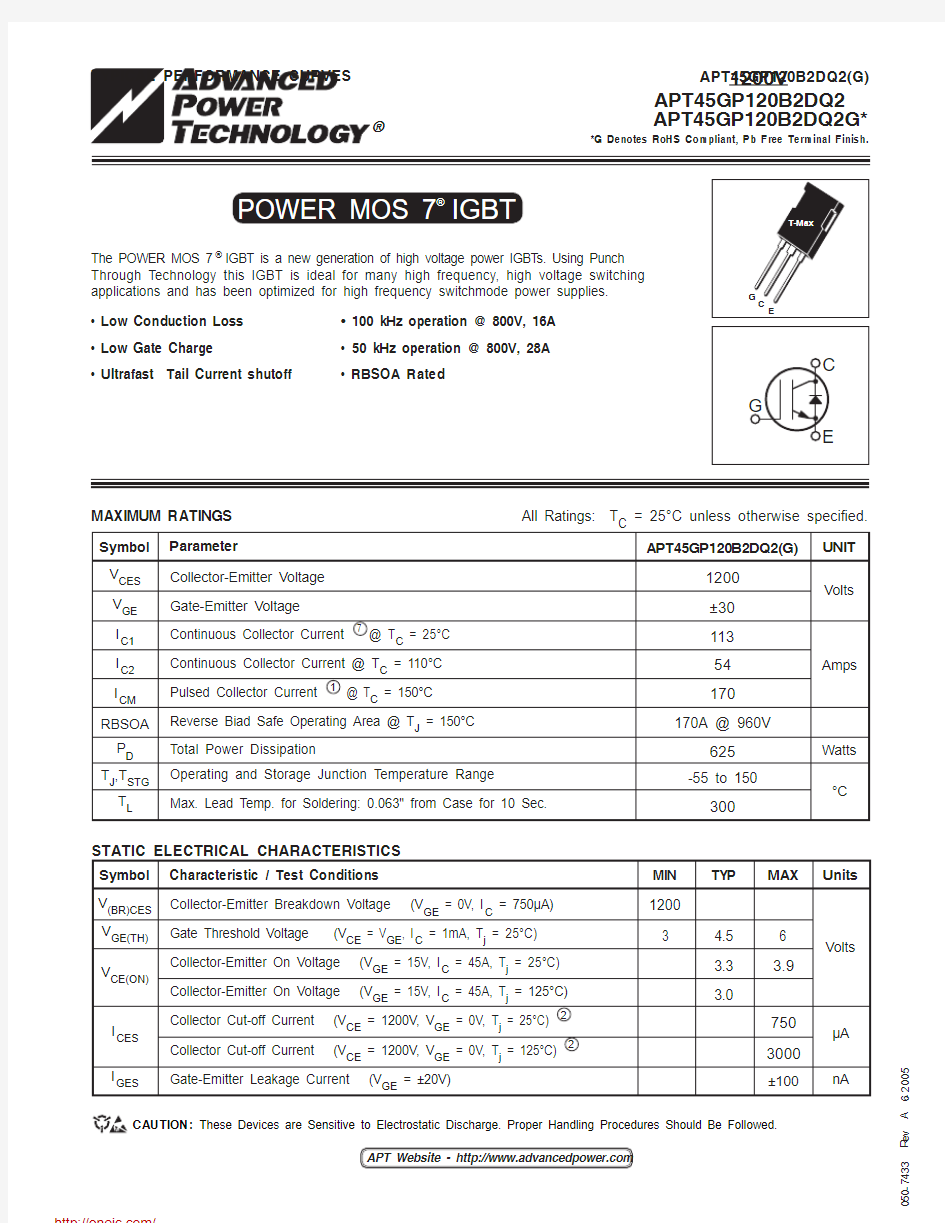
POWER MOS 7?
IGBT
https://www.doczj.com/doc/9314548641.html,/
050-7433 R e v A 6-2005
APT45GP120B2DQ2(G)
1 Repetitive Rating: Pulse width limited by maximum junction temperature.
2 For Combi devices, I ces includes both IGBT and FRED leakages
3 See MIL-STD-750 Method 3471.
4 E on1 is the clam ped inductive turn-on-energy of the IGBT only, without the effect of a commutating diode reverse recovery current adding to the IGBT turn-on loss. (See Figure 24.)
5 E on2 is the clamped inductive turn-on energy that includes a commutating diode reverse recovery current in the IGBT turn-on switching
loss. (See Figures 21, 22.)
6 E off is the clamped inductive turn-off energy measured in accordance with JEDEC standard JESD24-1. (See Figures 21, 23.)
7 Continuous current limited by package lead temperature.
APT Reserves the right to change, without notice, the speci?cations and information contained herein.
THERMAL AND MECHANICAL CHARACTERISTICS
UNIT °C/W gm
MIN TYP MAX
.20 .61
5.9
Characteristic
Junction to Case (IGBT)Junction to Case (DIODE)Package Weight
Symbol R θJC R θJC W T
DYNAMIC CHARACTERISTICS
Symbol C ies C oes C res V GEP Q g Q ge Q gc RBSOA t d(on)t r
t d(off)t f E on1E on2E off t d(on)t r t d(off)t f E on1E on2E off Test Conditions Capacitance V GE = 0V, V CE = 25V
f = 1 MHz Gate Charge V GE = 15V
V CE = 600V I C = 45A
T J = 150°C, R G = 5?, V GE =
15V, L = 100μH,V CE = 960V Inductive Switching (25°C)V CC = 600V V GE = 15V I C = 45A R G = 5?
T J = +25°C
Inductive Switching (125°C)V CC =600V V GE = 15V I C = 45A R G = 5?
T J = +125°C
Characteristic Input Capacitance Output Capacitance
Reverse Transfer Capacitance Gate-to-Emitter Plateau Voltage Total Gate Charge 3 Gate-Emitter Charge
Gate-Collector ("Miller") Charge Reverse Bias Safe Operating Area Turn-on Delay Time Current Rise Time Turn-off Delay Time Current Fall Time
Turn-on Switching Energy 4
Turn-on Switching Energy (Diode) 5Turn-off Switching Energy 6 Turn-on Delay Time Current Rise Time Turn-off Delay Time Current Fall Time
Turn-on Switching Energy 4 4
Turn-on Switching Energy (Diode) 55Turn-off Switching Energy 6
MIN TYP
MAX
3995 300 55 7.5 185 25
80 170
18
29 100 38 900 1870
905
18
29 150
80 900 3080
2255
UNIT pF V nC
A
ns
μJ
ns μJ
https://www.doczj.com/doc/9314548641.html,/
050-7433 R e v A 6-2005
B V
C E S , C O L L E C T O R -T O -E M I T T E R B R E A K
D O W N V C
E , C O L L E C T O R -T O -E M I T T E R V O L T A G E (V )
I C , C O L L E C T O R C U R R E N T (
A )
I C , C O
L L E C T O R C U R R
E N T (A )
V O
L T A G E (N O R M A L I Z E D )
I C , D C C O L L E C T O R C U R R E N T (A ) V C E , C O L L E C T O R -T O -E M I T T E R V O L T A G E (V ) V G E , G A T E -T O -E M I T T E R V O L T A G E (V )
I C , C O L L E C T O R C U R R E N T (A )
1.20
1.151.101.051.000.950.900.85
0.80
V CE , COLLECTER-TO-EMITTER VOLTAGE (V)
V CE , COLLECTER-TO-EMITTER VOLTAGE (V)
FIGURE 1, Output Characteristics(T J = 25°C)
FIGURE 2, Output Characteristics (T J = 125°C)
V GE , GATE-TO-EMITTER VOLTAGE (V) GATE CHARGE (nC)
FIGURE 3, Transfer Characteristics
FIGURE 4, Gate Charge
V GE , GATE-TO-EMITTER VOLTAGE (V)
T J , Junction Temperature (°C)
FIGURE 5, On State Voltage vs Gate-to- Emitter Voltage FIGURE 6, On State Voltage vs Junction Temperature T J , JUNCTION TEMPERATURE (°C)
T C , CASE TEMPERATURE (°C)
FIGURE 7, Breakdown Voltage vs. Junction Temperature
FIGURE 8, DC Collector Current vs Case Temperature
https://www.doczj.com/doc/9314548641.html,/
050-7433 R e v A 6-2005
S W I T C H I N G E N E R G Y L O S S E S (μJ ) E O N 2, T U R N O
N E N E R G Y L O S S (μJ )
t r , R I S E T I M E (
n s )
t d (O N ), T U R N
-O N D E L A Y T I M E (n s )
S W I T C H I N G E N E
R G Y L O S S E S (μJ ) E O F F , T U R N O F F
E N E R G Y L O S S (μJ )
t f , F A L L T I M E (n s )
t d (O F F ), T U R N -O F F D E L A Y T I M E (n s )
I CE , COLLECTOR TO EMITTER CURRENT (A) I CE , COLLECTOR TO EMITTER CURRENT (A)
FIGURE 9, Turn-On Delay Time vs Collector Current
FIGURE 10, Turn-Off Delay Time vs Collector Current
I CE , COLLECTOR TO EMITTER CURRENT (A) I CE , COLLECTOR TO EMITTER CURRENT (A)
FIGURE 11, Current Rise Time vs Collector Current
FIGURE 12, Current Fall Time vs Collector Current
I CE , COLLECTOR TO EMITTER CURRENT (A)
I CE , COLLECTOR TO EMITTER CURRENT (A)
FIGURE 13, Turn-On Energy Loss vs Collector Current
FIGURE 14, Turn Off Energy Loss vs Collector Current
R G , GATE RESISTANCE (OHMS)
T J , JUNCTION TEMPERATURE (°C)
FIGURE 15, Switching Energy Losses vs. Gate Resistance
FIGURE 16, Switching Energy Losses vs Junction Temperature
25
20
15
10
50
8070605040302010
80007000600050004000300020001000
12000100008000600040002000
180160140120100806040
200
100
80
60
40
20
600050004000300020001000
80007000600050004000300020001000
https://www.doczj.com/doc/9314548641.html,/
050-7433 R e v A 6-2005
APT45GP120B2DQ2(G)
Z θJ C , T H E R M A L I M P E D A N C E (°C /W )
RECTANGULAR PULSE DURATION (SECONDS)
Figure 19a, Maximum Effective Transient Thermal Impedance, Junction-To-Case vs Pulse Duration
18016014012010080604020
C , C A P A C I T A N C E (P
F )
I C , C O L L E C T O R C U R R E N T (A )
V CE , COLLECTOR-TO-EMITTER VOLTAGE (VOLTS) V CE , COLLECTOR TO EMITTER VOLTAGE
Figure 17, Capacitance vs Collector-To-Emitter Voltage
Figure 18,Minimim Reverse Bias Safe Operating Area
0 100 200 300 400 500 600 700 800 900 1000FIGURE 19b, TRANSIENT THERMAL IMPEDANCE MODEL
F M A X , O P E R A T I N
G F R E Q U E N C Y (k
H z )
I C , COLLECTOR CURRENT (A) Figure 20, Operating Frequency vs Collector Current
0.000782
0.0150
0.185
Junction temp. (°C)
RC MODEL
Case temperature. (°https://www.doczj.com/doc/9314548641.html,/
050-7433 R e v A 6-2005
APT45GP120B2DQ2(G)
Figure 22, Turn-on Switching Waveforms and De?nitions
Figure 23, Turn-off Switching Waveforms and De?nitions
V
Figure 24, E ON1 Test Circuit
Gate Voltage
Collector Voltage
Collector Current
90%
Switching Energy
T J = 125 °C
90%
t d(off)
t f
10%
10%
t d(on)
5%
10%
90%
t r
5 %
Collector Current
Collector Voltage
Gate Voltage
Switching Energy
T J = 125 °C
https://www.doczj.com/doc/9314548641.html,/
050-7433 R e v A 6-2005
APT45GP120B2DQ2(G)
TYPICAL PERFORMANCE CURVES Characteristic / Test Conditions
Maximum Average Forward Current (T C = 112°C, Duty Cycle = 0.5)RMS Forward Current (Square wave, 50% duty)
Non-Repetitive Forward Surge Current (T J = 45°C, 8.3ms)Symbol I F (AV)I F (RMS)I FSM Symbol V F
Characteristic / Test Conditions
I F = 45A Forward Voltage I F = 90A
I F = 40A, T J = 125°C
STATIC ELECTRICAL CHARACTERISTICS
UNIT
Amps
UNIT
Volts MIN
TYP
MAX
2.9
3.56
2.28
APT45GP120B2DQ2(G)4063210
DYNAMIC CHARACTERISTICS
MAXIMUM RATINGS
All Ratings: T C = 25°C unless otherwise speci?ed.
ULTRAFAST SOFT RECOVERY ANTI-PARALLEL DIODE
MIN
TYP
MAX
-
26
- 350 - 570 - 4 -
- 430 - 2200 - 9 - - 210 - 3400
-
29
UNIT ns nC
Amps ns nC Amps ns nC Amps
Characteristic
Reverse Recovery Time Reverse Recovery Time Reverse Recovery Charge
Maximum Reverse Recovery Current Reverse Recovery Time Reverse Recovery Charge
Maximum Reverse Recovery Current Reverse Recovery Time Reverse Recovery Charge
Maximum Reverse Recovery Current
Symbol t rr t rr Q rr I RRM t rr Q rr I RRM t rr Q rr I RRM
Test Conditions
I F = 40A, di F /dt = -200A/μs V R = 800V, T C = 25°C
I F = 40A, di F /dt = -200A/μs V R = 800V, T C = 125°C
I F = 40A, di F /dt = -1000A/μs V R = 800V, T C = 125°C
I F = 1A, di F /dt = -100A/μs, V R = 30V, T J = 25°C
Z θJ C , T H E R M A L I M P E D A N C E (°C /W )
RECTANGULAR PULSE DURATION (seconds)
FIGURE 25a. MAXIMUM EFFECTIVE TRANSIENT THERMAL IMPEDANCE, JUNCTION-TO-CASE vs. PULSE DURATION
0.00222 J/°C
0.00586 J/°C
0.0596 J/°C
Junction temp (°RC MODEL
Case temperature (°https://www.doczj.com/doc/9314548641.html,/
050-7433 R e v A 6-2005
APT45GP120B2DQ2(G)
C J , J U N C T I O N C A P A C I T A N C E K f ,
D Y N A M I C P A R A M
E T E R S
(p F )
(N o r m a l i z e d t o 1000A /μs )
I F (A V ) (A )
T J , JUNCTION TEMPERATURE (°C)
Case Temperature (°C)
Figure 30. Dynamic Parameters vs. Junction Temperature
Figure 31. Maximum Average Forward Current vs. CaseTemperature
V R , REVERSE VOLTAGE (V)
Figure 32. Junction Capacitance vs. Reverse Voltage
V F , ANODE-TO-CATHODE VOLTAGE (V)
-di F /dt, CURRENT RATE OF CHANGE(A/μs)
Figure 26. Forward Current vs. Forward Voltage
Figure 27. Reverse Recovery Time vs. Current Rate of Change -di F /dt, CURRENT RATE OF CHANGE (A/μs)
-di F /dt, CURRENT RATE OF CHANGE (A/μs)
Figure 28. Reverse Recovery Charge vs. Current Rate of Change
Figure 29. Reverse Recovery Current vs. Current Rate of Change
Q r r , R E V E R S E R E C O V E R Y C H A R G E I F , F O R W A R D C U R R E N T
(n C )
(A )
I R R M , R E V E R S E R E C O V E R Y C U R R E N T t r r , R E V E R S E R E C O V E R Y T I M E
(A )
(n s )
200
150
100
50
1
10 100 200
https://www.doczj.com/doc/9314548641.html,/
050-7433 R e v A 6-2005
APT45GP120B2DQ2(G)
TYPICAL PERFORMANCE CURVES
5
1234
di F /dt - Rate of Diode Current Change Through Zero Crossing.I F - Forward Conduction Current
I RRM - Maximum Reverse Recovery Current.
t
rr - Reverse R ecovery Time, measured from zero crossing where Q rr - Area Under the Curve Defined by I RRM and t rr .
line through I RRM and 0.25 I RRM passes through zero.Figure 33. Diode Test Circui t
Figure 34, Diode Reverse Recovery Waveform and Definitions
APT’s products are covered by one or more of U.S.patents 4,895,810 5,045,903 5,089,434 5,182,234 5,019,522
5,262,336 6,503,786 5,256,583 4,748,103 5,283,202 5,231,474 5,434,095 5,528,058 and foreign patents. US and Foreign patents pending. All Rights Reserved.
e1SAC: Tin, Silver, Copper
T-MAX? (B2) Package Outline
Dimensions in Millimeters and (Inches)
https://www.doczj.com/doc/9314548641.html,/
分销商库存信息: MICROSEMI
APT45GP120B2DQ2G