For free samples and the latest literature, visit https://www.doczj.com/doc/9b11132110.html, or phone 1-800-998-8800.For small orders, phone 1-800-835-8769.
General Description
The MAX1084/MAX1085 10-bit analog-to-digital convert-ers (ADCs) combine a high-bandwidth track/hold, a serial interface with high conversion speed, an internal +2.5V reference, and low power consumption. The MAX1084operates from a single +4.5V to +5.5V supply; the MAX1085 operates from a single +2.7V to +3.6V supply. The 3-wire serial interface connects directly to SPI?/QSPI?/MICROWIRE? devices without external logic. The devices use an external serial-interface clock to perform successive-approximation analog-to-digital con-versions.
Low power combined with ease of use and small pack-age size make these converters ideal for remote-sensor and data-acquisition applications, or for other circuits with demanding power consumption and space requirements.The MAX1084/MAX1085 are available in 8-pin SO packages.
These devices are pin-compatible, higher-speed versions of the MAX1242/MAX1243; for more information, refer to the respective data sheets.
Applications
Portable Data Logging Data Acquisition Medical Instruments Battery-Powered Instruments Pen Digitizers Process Control
Features
o Single-Supply Operation
+4.5V to +5.5V (MAX1084)+2.7V to +3.6V (MAX1085)o 10-Bit Resolution
o 400ksps Sampling Rate (MAX1084)o Internal Track/Hold o Internal +2.5V Reference o Low Power: 2.5mA (400ksps)
o SPI/QSPI/MICROWIRE 3-Wire Serial Interface o Pin-Compatible, High-Speed Upgrade to MAX1242/MAX1243o 8-Pin SO Package
MAX1084/MAX1085
400ksps/300ksps, Single-Supply, Low-Power, Serial 10-Bit ADCs with Internal Reference
________________________________________________________________Maxim Integrated Products 1
19-1686; Rev 0; 5/00
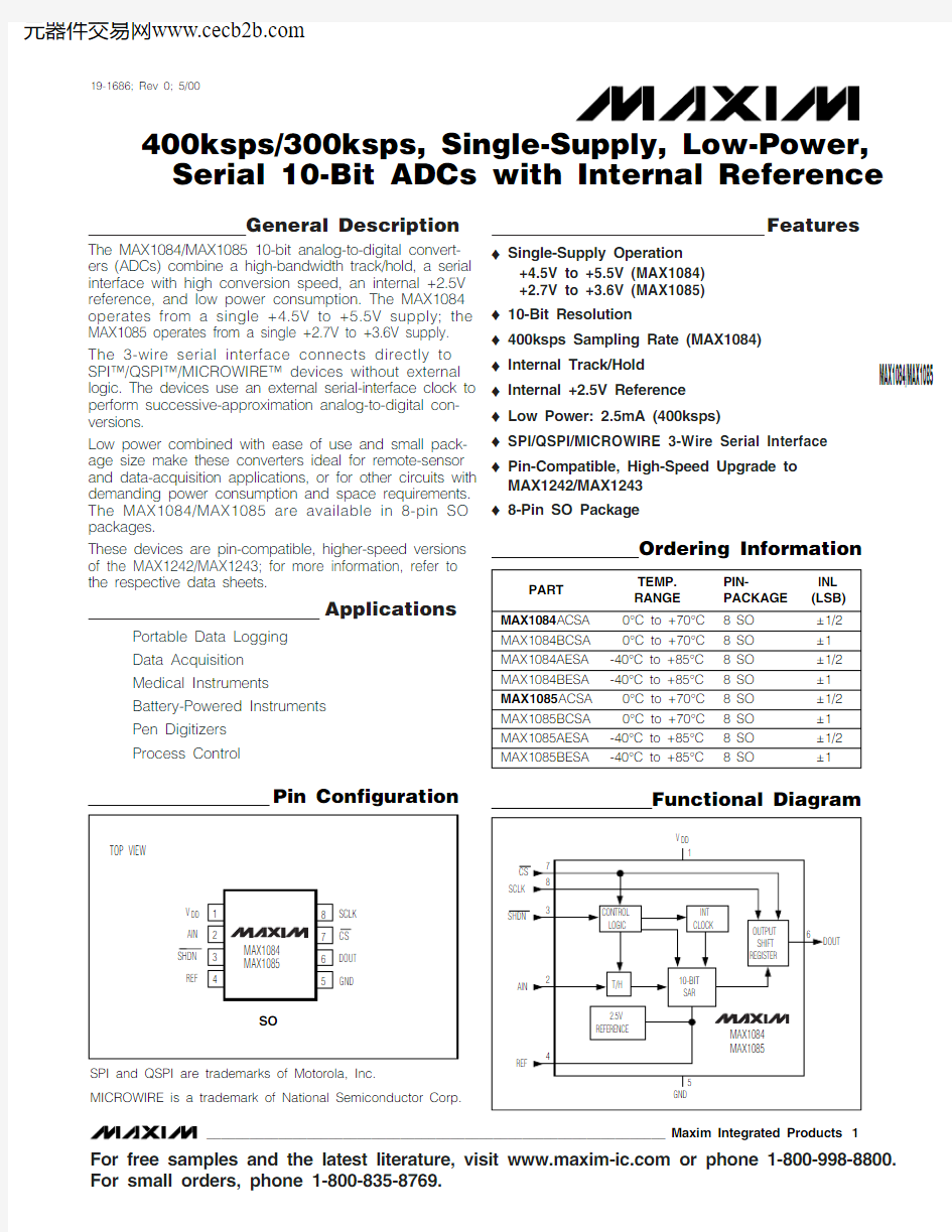
Pin Configuration
Ordering Information
SPI and QSPI are trademarks of Motorola, Inc.
MICROWIRE is a trademark of National Semiconductor Corp.
M A X 1084/M A X 1085
400ksps/300ksps, Single-Supply, Low-Power, Serial 10-Bit ADCs with Internal Reference 2_______________________________________________________________________________________
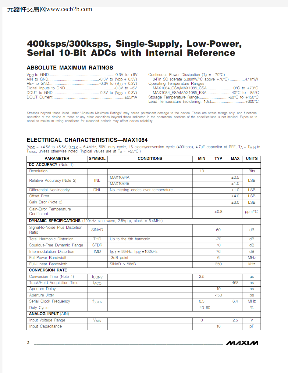
ABSOLUTE MAXIMUM RATINGS
ELECTRICAL CHARACTERISTICS—MAX1084
(V DD = +4.5V to +5.5V, f SCLK = 6.4MHz, 50% duty cycle, 16 clocks/conversion cycle (400ksps), 4.7μF capacitor at REF, T A = T MIN to T MAX , unless otherwise noted. Typical values are at T A = +25°C.)
Stresses beyond those listed under “Absolute Maximum Ratings” may cause permanent damage to the device. These are stress ratings only, and functional operation of the device at these or any other conditions beyond those indicated in the operational sections of the specifications is not implied. Exposure to absolute maximum rating conditions for extended periods may affect device reliability.
V DD to GND.............................................................-0.3V to +6V AIN to GND................................................-0.3V to (V DD + 0.3V)REF to GND...............................................-0.3V to (V DD + 0.3V)Digital Inputs to GND...............................................-0.3V to +6V DOUT to GND............................................-0.3V to (V DD + 0.3V)DOUT Current..................................................................±25mA
Continuous Power Dissipation (T A = +70°C)
8-Pin SO (derate 5.88mW/°C above +70°C)..............471mW Operating Temperature Ranges
MAX1084_CSA/MAX1085_CSA.........................0°C to +70°C MAX1084_ESA/MAX1085_ESA......................-40°C to +85°C Storage Temperature Range............................-60°C to +150°C Lead Temperature (soldering, 10s)................................+300°C
MAX1084/MAX1085
400ksps/300ksps, Single-Supply, Low-Power, Serial 10-Bit ADCs with Internal Reference
ELECTRICAL CHARACTERISTICS—MAX1084 (continued)
(V DD = +4.5V to +5.5V, f SCLK = 6.4MHz, 50% duty cycle, 16 clocks/conversion cycle (400ksps), 4.7μF capacitor at REF, T A = T MIN to T MAX , unless otherwise noted. Typical values are at T A = +25°C.)
ELECTRICAL CHARACTERISTICS—MAX1085
(V DD = +2.7V to +3.6V, f SCLK = 4.8MHz, 50% duty cycle, 16 clocks/conversion cycle (300ksps), 4.7μF capacitor at REF, T A = T MIN to T MAX , unless otherwise noted. Typical values are at T A = +25°C.)
M A X 1084/M A X 1085
400ksps/300ksps, Single-Supply, Low-Power, Serial 10-Bit ADCs with Internal Reference
ELECTRICAL CHARACTERISTICS—MAX1085 (continued)
(V DD = +2.7V to +3.6V, f SCLK = 4.8MHz, 50% duty cycle, 16 clocks/conversion cycle (300ksps), 4.7μF capacitor at REF, T A = T MIN to T MAX , unless otherwise noted. Typical values are at T A = +25°C.)
MAX1084/MAX1085
400ksps/300ksps, Single-Supply, Low-Power, Serial 10-Bit ADCs with Internal Reference
_______________________________________________________________________________________5
TIMING CHARACTERISTICS—MAX1084
(Figures 1, 2, 8, 9; V DD = +4.5V to +5.5V, T A = T MIN to T MAX , unless otherwise noted.)
TIMING CHARACTERISTICS—MAX1085
(Figures 1, 2, 8, 9; V DD = +2.7V to +3.6V, T A = T MIN to T MAX , unless otherwise noted.)
Note 1:Tested at V DD = V DD,MIN .
Note 2:Relative accuracy is the deviation of the analog value at any code from its theoretical value after the full-scale range has
been calibrated.
Note 3:Internal reference, offset, and reference errors nulled.
Note 4:Conversion time is defined as the number of clock cycles multiplied by the clock period; clock has 50% duty cycle.
Note 5:External load should not change during conversion for specified accuracy. Guaranteed specification limit of 2mV/mA due to
production test limitation.
Note 6:Electrical characteristics are guaranteed from V DD,MIN to V DD,MAX . For operations beyond this range, see Typical Operating
Characteristics.
Note 7:MAX1084 tested with 20pF on DOUT and f SCLK = 6.4MHz, 0 to 5V. MAX1085 tested with same loads, f SCLK = 4.8MHz, 0 to
3V. DOUT = full scale.
M A X 1084/M A X 1085
400ksps/300ksps, Single-Supply, Low-Power, Serial 10-Bit ADCs with Internal Reference 6
_______________________________________________________________________________________
-0.10
-0.04-0.06-0.08-0.0200.020.04
0.060.080.100
400
200
600
800
1000
1200
INTEGRAL NONLINEARLITY vs. DIGITAL OUTPUT CODE
M A X 1084/5t o c 01
DIGITAL OUTPUT CODE
I N L (L S B )
-0.15
-0.05-0.100.050
0.100.150
400
600
200
800
1000
1200
DIFFERENTIAL NONLINEARITY vs. DIGITAL OUTPUT CODE
M A X 1084/5t o c 02
DIGITAL OUTPUT CODE
D N L (L S B )
-0.25
0.25
0.50
2.5
4.0
4.5
3.0
3.5
5.0
5.5
6.0
OFFSET ERROR vs. SUPPLY VOLTAGE
M A X 1084/5 t o c 03
V DD (V)
O F F S E T E R R O R (L S B )
00.100.050.250.200.150.400.350.300.45-40
20
-20
40
60
80
100OFFSET ERROR vs. TEMPERATURE
M A X 104/5 t o c 04
TEMPERATURE (°C)O F F S E T E R R O R (L S B )-0.25
-0.10-0.15-0.20-0.0500.050.100.150.200.252.5 3.53.0 4.0 4.5 5.0 5.5GAIN ERROR vs. SUPPLY VOLTAGE
M A X 1084/5 t o c 05
V DD (V)
G A I N E R R O R (L S B )
-0.50
-0.25
0.25
-40020-20406080100
GAIN ERROR vs. TEMPERATURE
M A X 1084/5 t o c 06
TEMPERATURE (°C)
G A I N E R R O R (L S B )
Typical Operating Characteristics
(MAX1084: V DD = +5.0V, f SCLK = 6.4MHz; MAX1055: V DD = +3.0V, f SCLK = 4.8MHz; C LOAD = 20pF, 4.7μF capacitor at REF, T A = +25°C, unless otherwise noted.)
MAX1084/MAX1085
400ksps/300ksps, Single-Supply, Low-Power, Serial 10-Bit ADCs with Internal Reference
2.490
2.4962.4942.4922.4982.5002.5022.5042.5062.5082.5102.5
3.5
3.0
4.0
4.5
5.0
5.5INTERNAL REFERENCE VOLTAGE
vs. SUPPLY VOLTAGE
M A X 1084/5 t o c 07
SUPPLY VOLTAGE (V)V R E F (V ) 2.490
2.4962.4942.4922.5002.4982.5082.5062.5042.5022.510
-40-20020406080100
INTERNAL REFERENCE VOLTAGE
vs. TEMPERATURE
M A X 1084/5 t o c 08
TEMPERATURE (°C)
V R E F (V )1.50
2.001.752.502.252.75
3.002.5
3.5
4.0
3.0
4.5
5.0
5.5
SUPPLY CURRENT vs. SUPPLY VOLTAGE
SUPPLY VOLTAGE (V)
S U P P L Y C U R R E N T (m A ) 1.5
1.8
2.4
2.1
2.7
3.0
-40
-20
20
40
60
80
100
SUPPLY CURRENT vs. TEMPERATURE
TEMPERATURE (°C)
S U P P L Y C U R R E N T (m A )
Typical Operating Characteristics (continued)
(MAX1084: V DD = +5.0V, f SCLK = 6.4MHz; MAX1085: V DD = +3.0V, f SCLK = 4.8MHz; C LOAD = 20pF, 4.7μF capacitor at REF, T A = +25°C, unless otherwise noted.)
Pin Description
M A X 1084/M A X 1085
400ksps/300ksps, Single-Supply, Low-Power, Serial 10-Bit ADCs with Internal Reference 8
_______________________________________________________________________________________
_______________Detailed Description
Converter Operation
The MAX1084/MAX1085 use an input track/hold (T/H)and successive-approximation register (SAR) circuitry to convert an analog input signal to a digital 10-bit output.Figure 3 shows the MAX1084/MAX1085 in their simplest configuration. The internal reference is trimmed to 2.5V.The serial interface requires only three digital lines (SCLK, CS ,and DOUT) and provides an easy interface to microprocessors (μPs).
The MAX1084/MAX1085 have two modes: normal and shutdown. Pulling SHDN low shuts the device down and reduces supply current to 2μA (typ); pulling SHDN high puts the device into operational mode. Pulling CS low ini-tiates a conversion that is driven by SCLK. The conver-sion result is available at DOUT in unipolar serial format.The serial data stream consists of three zeros, followed by the data bits (MSB first). All transitions on DOUT occur 20ns after the rising edge of SCLK.Figures 8 and 9 show the interface timing information.
Analog Input
Figure 4 shows the sampling architecture of the ADC’s comparator. The full-scale input voltage is set by the internal reference (V REF = +2.5V).
Track/Hold
In track mode, the analog signal is acquired and stored in the internal hold capacitor. In hold mode, the T/H switch opens and maintains a constant input to the ADC’s SAR section.
During acquisition, the analog input AIN charges capacitor C HOLD . Bringing CS low ends the acquisition interval. At this instant, the T/H switches the input side of C HOLD to GND. The retained charge on C HOLD repre-sents a sample of the input, unbalancing node ZERO at the comparator’s input.
In hold mode, the capacitive digital-to-analog converter (DAC) adjusts during the remainder of the conversion cycle to restore node ZERO to 0 within the limits of 10-bit resolution. This action is equivalent to transferring a charge from C HOLD to the binary-weighted capacitive
Figure 1. Load Circuits for DOUT Enable Time
Figure 2. Load Circuits for DOUT Disable Time
MAX1084/MAX1085
400ksps/300ksps, Single-Supply, Low-Power, Serial 10-Bit ADCs with Internal Reference
_______________________________________________________________________________________
9
DAC, which in turn forms a digital representation of the analog input signal. At the conversion’s end, the input side of C HOLD switches back to AIN, and C HOLD charges to the input signal again.
The time required for the T/H to acquire an input signal is a function of how quickly its input capacitance is charged. If the input signal’s source impedance is high,the acquisition time lengthens, and more time must be allowed between conversions. The acquisition time,t ACQ , is the maximum time the device takes to acquire the signal and the minimum time needed for the signal to be acquired. Acquisition time is calculated by:
t ACQ = 7(R S + R IN ) ?12pF
where R IN = 800?, R S = the input signal’s source impedance, and t ACQ is never less than 468ns (MAX1284) or 625ns (MAX1085). Source impedance below 4k ?does not significantly affect the ADC’s AC performance.
Higher source impedances can be used if a 0.01μF capacitor is connected to the analog input. Note that the input capacitor forms an RC filter with the input source impedance, limiting the ADC’s input signal bandwidth.
Input Bandwidth
The ADC’s input tracking circuitry has a 6MHz (MAX1084) or 3MHz (MAX1085) small-signal band-width, so it is possible to digitize high-speed transient events and measure periodic signals with bandwidths exceeding the ADC’s sampling rate by using under-sampling techniques. To avoid aliasing of unwanted high-frequency signals into the frequency band of inter-est, anti-alias filtering is recommended.
Analog Input Protection
Internal protection diodes, which clamp the analog input to V DD and G ND, allow the input to swing from GND - 0.3V to V DD + 0.3V without damage.
If the analog input exceeds 50mV beyond the supplies,limit the input current to 2mA.
Internal Reference
The MAX1084/MAX1085 have an on-chip voltage refer-ence trimmed to 2.5V. The internal reference output is connected to REF and also drives the internal capacitive DAC. The output can be used as a reference voltage source for other components and can source up to 800μA. Bypass REF with a 4.7μF capacitor. Larger capacitors increase wake-up time when exiting shut-down (see Using SHDN to Reduce Supply Current ). The internal reference is disabled in shutdown (SHDN = 0).
Serial Interface
Initialization After Power-Up and
Starting a Conversion
When power is first applied, and if SHDN is not pulled low, it takes the fully discharged 4.7μF reference bypass capacitor up to 1.4ms to acquire adequate charge for specified accuracy. No conversions should be performed during this time.
Figure 3. Typical Operating Circuit
Figure 4. Equivalent Input Circuit
M A X 1084/M A X 1085
400ksps/300ksps, Single-Supply, Low-Power, Serial 10-Bit ADCs with Internal Reference 10
______________________________________________________________________________________
To start a conversion, pull CS low. At CS ’s falling edge,the T/H enters its hold mode and a conversion is initiat-ed. Data can then be shifted out serially with the exter-nal clock.
Using S H D N to Reduce Supply Current
Power consumption can be reduced significantly by shutting down the MAX1084/MAX1085 between conver-sions. Figure 6 shows a plot of average supply current vs. conversion rate. The wake-up time, t WAKE , is the time from SHDN deasserted to the time when a conver-sion may be initiated (Figure 5).This time depends on the time in shutdown (Figure 7) because the external 4.7μF reference bypass capacitor loses charge slowly during shutdown and can be as long as 1.4ms.
Timing and Control
Conversion-start and data-read operations are con-trolled by the CS and SCLK digital inputs. The timing diagrams of Figures 8 and 9 outline serial-interface operation.
A CS falling edge initiates a conversion sequence: the T/H stage holds the input voltage, the ADC begins to convert, and DOUT changes from high impedance to logic low. SCLK is used to drive the conversion process, and it shifts data out as each bit of conversion is determined.
SCLK begins shifting out the data after the rising edge of the third SCLK pulse. DOUT transitions 20ns after each SCLK rising edge. The third rising clock edge produces the MSB of the conversion at DOUT, followed by the remaining bits. Since there are 12 data bits and 3 leading zeros, at least 15 rising clock edges are
needed to shift out these bits. Extra clock pulses occur-ring after the conversion result has been clocked out,and prior to a rising edge of CS , produce trailing zeros at DOUT and have no effect on converter operation.Pull CS high after reading the conversion’s LSB. For maximum throughput, CS can be pulled low again to ini-tiate the next conversion immediately after the specified minimum time (t CS ).
Output Coding and Transfer Function
The data output from the MAX1084/MAX1085 is binary.Figure 10 depicts the nominal transfer function. Code transitions occur halfway between successive-integer LSB values; V REF = 2.5V, and 1LSB = 2.44mV or 2.5V /1024.
Applications Information
Connection to Standard Interfaces
The MAX1084/MAX1085 serial interface is fully compat-ible with SPI, QSPI, and MICROWIRE (Figure 11).If a serial interface is available, set the CPU’s serial interface in master mode so the CPU generates the ser-ial clock. Choose a clock frequency up to 6.4MHz (MAX1084) or 4.8MHz (MAX1085).
1) Use a general-purpose I/O line on the CPU to pull CS low. Keep SCLK low.
2)Activate SCLK for a minimum of 13 clock cycles. The first two clocks produce zeros at DOUT. DOUT output data transitions 20ns after SCLK rising edge and is available in MSB-first format. Observe the SCLK-to-DOUT valid timing characteristic. Data can be clocked into the μP on SCLK’s falling or rising edge.
Figure 5. Shutdown Sequence
MAX1084/MAX1085
400ksps/300ksps, Single-Supply, Low-Power, Serial 10-Bit ADCs with Internal Reference
______________________________________________________________________________________11
Figure 7. Reference Power-Up vs. Time in Shutdown
Figure 8. Interface Timing Sequence
M A X 1084/M A X 1085
400ksps/300ksps, Single-Supply, Low-Power, Serial 10-Bit ADCs with Internal Reference 12
______________________________________________________________________________________
3) Pull CS high at or after the 13th rising clock edge. If CS remains low, the two sub-bits and trailing zeros are clocked out after the LSB.
4) With CS = high, wait the minimum specified time, t CS ,before initiating a new conversion by pulling CS low.If a conversion is aborted by pulling CS high before the conversion completes, wait the minimum acquisi-tion time, t ACQ , before starting a new conversion. CS must be held low until all data bits are clocked out.Data can be output in 2 bytes or continuously, as shown in Figure 8. The bytes contain the result of the conversion padded with three leading zeros, 2 sub-bits, and trailing zeros if SCLK is still active with CS kept low.
SPI and Microwire
When using SPI or QSPI, set CPOL = 0 and CPHA = 0.Conversion begins with a CS falling edge. DOUT goes low, indicating a conversion is in progress. Two con-secutive 1-byte reads are required to get the full 10+2bits from the ADC. DOUT output data transitions on SCLK’s rising edge and is clocked into the μP on the following rising edge.
The first byte contains 3 leading zeros, and 5 bits of conversion result. The second byte contains the remain-ing 5 bits, 2 sub-bits, and 1 trailing zero. See Figure 11for connections and Figure 12 for timing.
QSPI
Unlike SPI, which requires two 1-byte reads to acquire
the 10 bits of data from the ADC, QSPI allows the mini-mum number of clock cycles necessary to clock in the data. The MAX1084/MAX1085 require 13 clock cycles from the μP to clock out the 10 bits of data. Additional clock cycles clock out the 2 sub-bits followed by trailing zeros. Figure 13 shows a transfer using CPOL = 0 and CPHA = 1. The result of conversion contains two zeros followed by the 10 bits of data in MSB-first format.
Layout and Grounding
For best performance, use PC boards. Wire-wrap boards are not recommended. Board layout should ensure that digital and analog signal lines are separat-ed from each other. Do not run analog and digital (especially clock) lines parallel to one another, or digital lines underneath the ADC package.
Figure 14 shows the recommended system ground con-nections. Establish a single-point analog ground (“star”
Figure 10. Unipolar Transfer Function, Full Scale (FS) = V REF -1LSB, Zero Scale (ZS) = GND
Figure 11. Common Serial-Interface Connections to the MAX1084/MAX1085
MAX1084/MAX1085
400ksps/300ksps, Single-Supply, Low-Power, Serial 10-Bit ADCs with Internal Reference
______________________________________________________________________________________
13
ground point) at G ND, separate from the logic ground.Connect all other analog grounds and G ND to this star ground point for further noise reduction. No other digital system ground should be connected to this single-point analog ground. The ground return to the power supply for this ground should be low impedance and as short as possible for noise-free operation.
High-frequency noise in the V DD power supply may affect the ADC’s high-speed comparator. Bypass this supply to the single-point analog ground with 0.1μF and 10μF bypass capacitors. Minimize capacitor lead lengths for best supply-noise rejection. To reduce the effect of sup-ply noise, a 10?resistor can be connected as a lowpass filter to attenuate supply noise (Figure 14).
Definitions
Integral Nonlinearity
Integral nonlinearity (INL) is the deviation of the values on an actual transfer function from a straight line. This straight line can be either a best-straight-line fit or a line drawn between the endpoints of the transfer function,once offset and gain errors have been nullified. The
static linearity parameters for the MAX1084/MAX1085are measured using the endpoints method.
Differential Nonlinearity
Differential nonlinearity (DNL) is the difference between an actual step width and the ideal value of 1LSB. A DNL error specification of 1LSB or less guarantees no missing codes and a monotonic transfer function.
Aperture Jitter
Aperture jitter (t AJ ) is the sample-to-sample variation in the time between the samples.
Aperture Delay
Aperture delay (t AD ) is the time defined between the falling edge of CS and the instant when an actual sam-ple is taken.
Signal-to-Noise Ratio
For a waveform perfectly reconstructed from digital samples, signal-to-noise ratio (SNR) is the ratio of full-scale analog input (RMS value) to the RMS quantization error (residual error). The theoretical minimum analog-to-digital noise is caused by quantization error and results directly from the ADC’s resolution, (N bits):
Figure 12. SPI/MICROWIRE Serial Interface Timing (CPOL = CPHA = 0)
Figure 13. QSPI Serial Interface Timing (CPOL = 0, CPHA = 1)
M A X 1084/M A X 1085
400ksps/300ksps, Single-Supply, Low-Power, Serial 10-Bit ADCs with Internal Reference 14______________________________________________________________________________________
SNR = (6.02 ?N + 1.76)dB
In reality, there are other noise sources besides quanti-zation noise, including thermal noise, reference noise,clock jitter, etc. Therefore, SNR is computed by taking the ratio of the RMS signal to the RMS noise, which includes all spectral components minus the fundamen-tal, the first five harmonics, and the DC offset.
Signal-to-Noise Plus Distortion
Signal-to-noise plus distortion (SINAD) is the ratio of the fundamental input frequency’s RMS amplitude to RMS equivalent of all other ADC output signals.
SINAD (dB) = 20 ?log (SignalRMS / NoiseRMS)
Effective Number of Bits
Effective number of bits (ENOB) indicates the global accuracy of an ADC at a specific input frequency and sampling rate. An ideal ADC’s error consists of quanti-zation noise only. With an input range equal to the full-scale range of the ADC, calculate the effective number of bits as follows:
ENOB = (SINAD - 1.76) / 6.02
Total Harmonic Distortion
Total harmonic distortion (THD) is the ratio of the RMS sum of the first five harmonics of the input signal to the
where V1 is the fundamental amplitude, and V2 through V5 are the amplitudes of the 2nd- through 5th-order harmonics, respectively.
Spurious-Free Dynamic Range
Spurious-free dynamic range (SFDR) is the ratio of RMS amplitude of the fundamental (maximum signal compo-nent) to the RMS value of the next-largest distortion component.
___________________Chip Information
TRANSISTOR COUNT: 4286PROCESS: BiCMOS
Figure 14. Power-Supply Grounding Condition
MAX1084/MAX1085
400ksps/300ksps, Single-Supply, Low-Power, Serial 10-Bit ADCs with Internal Reference
______________________________________________________________________________________
15
________________________________________________________________Package Information
M A X 1084/M A X 1085
400ksps/300ksps, Single-Supply, Low-Power, Serial 10-Bit ADCs with Internal Reference Maxim cannot assume responsibility for use of any circuitry other than circuitry entirely embodied in a Maxim product. No circuit patent licenses are implied. Maxim reserves the right to change the circuitry and specifications without notice at any time.
16____________________Maxim Integrated Products, 120 San Gabriel Drive, Sunnyvale, CA 94086 408-737-7600?2000 Maxim Integrated Products
Printed USA
is a registered trademark of Maxim Integrated Products.
NOTES